New Perspectives on Surface Passivation:
Understanding the Si–Al
2
O
3
Interface
Lachlan E. Black
April 2015
The French chemists have given a new name to this pure earth; alumine in French, and alumina in Latin. I confess I do not like this alumina.
— Joseph Black
Declaration
The work in this thesis is my own except where otherwise stated.
Acknowledgements
Many people must be thanked for helping to bring this thesis to fruition, and helping me to survive it!
I have been extremely fortunate to have had a succession of outstanding men-tors who have helped to guide and shape me through my early research career. Firstly, I must thank Dr Keith McIntosh, my primary supervisor for the last four odd years and previously for my undergraduate thesis. I owe an enormous debt to Keith for originally stimulating my interest in photovoltaics research, and for do-ing so much to foster my abilities. Keith’s principled approach to scientific writdo-ing and research has been a huge influence on me, and his unfailing enthusiasm and encouragement have been a constant source of motivation. Our discussions were always a pleasure to partake in, and almost invariably produced fresh insights.
Another large debt is owed to Professor Andr´es Cuevas, who stepped in to assume a significant supervisory role in my PhD following Keith’s departure from ANU. Andr´es’ infectious enthusiasm and good humour, coupled with his immense knowledge of the field, have been a great source of support. His readiness to challenge conventional misconceptions is a particular source of inspiration.
Another early mentor who must be acknowledged is Dr Frank Lenzmann, who supervised me during my stay as an intern at ECN, prior to commencing my PhD. Frank allowed me a great deal of initiative in pursuing research objectives, giving me the space to spread my wings, and influenced my attitude to both life and research through his own example. His passionate commitment to renewable energy is an inspiration.
This project could not have been undertaken without the expert support of Ken Provancha, Jeff Simpson, and all the team at Schmid Thermal Systems (for-merly SierraTherm), in connection with the design, installation, operation, and maintenance of the prototype atmospheric pressure chemical vapour deposition (APCVD) Al2O3 deposition system at ANU. Ken in particular devoted countless hours to the design and testing of the system, and his invaluable advice helped
keep things running through thick and thin.
In the same vein, James Cotsell, perhaps the handiest man I know, provided invaluable technical support, and shared the many hours spent maintaining and trouble-shooting the APCVD system. James’ willing enthusiasm and relentless optimism were a great asset. Bruce Condon provided able assistance with all matters electrical, particularly with several technical aspects of the C–V mea-surement system.
A major mention must go to Thomas Allen who contributed invaluable prac-tical assistance with a number of experiments. This work would be significantly poorer without his many hours spent preparing samples and profiling diffusions. Many other colleagues gave freely of their time and expertise. I have benefited from discussions with and practical assistance from Simeon Baker-Finch, James Bullock, Andreas Fell, Nicholas Grant, Anthony Hill, Teng Kho, Wensheng Liang, Daniel Macdonald, Fiacre Rougieux, Pheng Phang, Andrew Thomson, Yimao Wan, Klaus Weber, Di Yan, and Xinyu Zhang, among others.
I have been fortunate to have had more than one opportunity to collabo-rate with colleagues at other research groups during the course of my PhD. In particular I would like to acknowledge Boris Veith at the Institut f¨ur Solaren-ergieforschung Hameln (ISFH), and Emanuele Cornagliotti at the Interuniversity Microelectronics Centre (IMEC) for their fruitful collaboration. Numerous other friends and colleagues at IMEC helped to make my stay there a highly enjoyable and profitable one.
I have made many friends during the course of my PhD, both at ANU and beyond. My fellow PhD students shared the ups and downs, and helped to keep me sane. I would particularly like to acknowledge Arnold McKinley and Chog Barugkin, with whom I shared many good times. More generally, I would like to acknowledge the many members of the solar research community at ANU, who made it such a rich and enjoyable place to work for four years. I have been privileged to be able to spend my time in such fine company. Our lunchtime conversations were often profound, and always entertaining.
Special thanks go to my girlfriend Melde for her patience and support, espe-cially during the final months of writing, when it looked like I’d never get there, and for helping to spur me on towards the finish line.
Abstract
High-efficiency crystalline silicon solar cells must suppress recombination at their
p-type surfaces. Thin-film, amorphous aluminium oxide (Al2O3) has been shown to provide very effective passivation of such surfaces, assisted by its negative fixed charge. However, many details of Al2O3 passivation remain poorly understood. Furthermore, conventional means of depositing passivating Al2O3 are too slow or too expensive to be suitable for high-volume commercial production.
This thesis addresses these issues in three ways: 1) by contributing to a deeper understanding of semiconductor–dielectric interfaces and semiconductor surface recombination mechanisms in general, 2) by investigating the properties of Al2O3 as a passivating dielectric for silicon surfaces, and 3) by demonstrating the viabil-ity of APCVD as a high-throughput, industrially compatible deposition method for Al2O3, enabling its application to commercial solar cells.
Using Al2O3 as a test case, it is shown how a novel analysis of the extended conductance method can be used to i) distinguish the separate contributions to the interface state distribution at a semiconductor-dielectric interface, and ii) determine their capture cross-sections for both minority and majority carriers. Furthermore, the direct link between these measured interface state properties and the recombination rate at the semiconductor surface is experimentally demon-strated by showing that the former can be used to accurately predict the latter.
Investigations of the surface passivation properties of Al2O3 reveal a remark-ably consistent picture. It is shown that the properties of the Si–Al2O3 interface states are essentially independent of the Al2O3 deposition conditions and tech-nique. The interface properties are found to be independent of the surface dopant concentration at boron- and phosphorus-doped surfaces, while recombination is shown to be only weakly dependent on surface orientation and morphology as a result of the remarkable orientation-independence of the Si–Al2O3 interface state properties. Meanwhile, the chemical origin of the charge at the Si–Al2O3interface is elucidated by correlating FTIR and electrical measurements.
APCVD is clearly shown—for the first time—to be capable of depositing Al2O3 films with exceptional surface passivation properties, comparable to the best results achieved using other deposition techniques. In the best case, interface state densities as low as 5×10¹⁰eV−1cm−2 at midgap, and negative fixed charge
concentrations of 3.3×1012cm−2 are measured, resulting in a saturation current
density of 7 fA cm−2 on undiffusedp-type surfaces. The APCVD films are shown
Contents
Acknowledgements ix
Abstract xi
List of Abbreviations xvii
List of Symbols xix
1 Introduction 1
1.1 Characterisation of surface passivation . . . 2
1.2 Al2O3 as a passivating dielectric . . . 4
1.3 Industrial application of Al2O3 . . . 7
1.4 Outline of this work . . . 9
2 Surface Recombination Theory 11 2.1 The semiconductor surface . . . 12
2.2 Definition of energies and potentials . . . 14
2.3 Surface charge and band-bending . . . 16
2.4 Recombination through defect states . . . 18
2.5 Surface recombination . . . 19
2.6 Relationship to experimental parameters . . . 23
3 Al2O3 Deposition and Characterisation 27 3.1 Al2O3 deposition by APCVD . . . 27
3.1.1 Deposition system . . . 28
3.1.2 Process parameters . . . 29
3.1.3 Chemical precursors . . . 30
3.1.4 Temperature profiles . . . 34
3.2 Sample preparation . . . 36
3.3 Characterisation . . . 37
4 Electrical Properties of the Si−Al2O3 Interface 41
4.1 Interface state distribution . . . 42
4.2 Capture cross-sections . . . 46
4.2.1 The conductance method . . . 46
4.2.2 Previous work . . . 48
4.2.3 Real and apparent capture cross-sections . . . 49
4.2.4 Determination of σp and σn . . . 53
4.2.5 Information from temperature-dependent measurements . 60 4.3 Comparison of model and experiment . . . 63
4.4 Conclusions . . . 66
5 Influence of Deposition Parameters 69 5.1 Substrate temperature . . . 69
5.1.1 H2O . . . 70
5.1.2 O2 . . . 71
5.2 Reactant concentration . . . 73
5.2.1 H2O . . . 74
5.2.2 O2 . . . 75
5.3 Chemical precursor . . . 76
5.4 Conclusions . . . 78
6 Effect of Post-Deposition Thermal Processing 81 6.1 Firing . . . 82
6.2 Rapid thermal annealing . . . 93
6.3 Conclusions . . . 100
7 Effect of Surface Dopant Concentration 103 7.1 Introduction . . . 103
7.2 Boron-doped surfaces . . . 105
7.3 Phosphorus-doped surfaces . . . 118
7.3.1 Undiffused surfaces . . . 119
7.3.2 Diffused surfaces . . . 126
7.4 Consequences for device design . . . 147
7.5 Conclusions . . . 149
8 Effect of Surface Orientation and Morphology 151 8.1 Recombination at h100i, h111i, and textured surfaces . . . 152
Contents xv
8.3 Conclusions . . . 164
9 Relationship Between Al2O3 Bulk and Interface Properties 165 9.1 Structure and composition . . . 166
9.1.1 Infrared absorption measurements . . . 166
9.1.2 Band assignments . . . 167
9.1.3 Trends and discussion . . . 173
9.2 Dielectric properties . . . 178
9.3 Optical properties . . . 182
9.4 Conclusions . . . 186
10 Conclusion 187 Appendix A Capacitance–Voltage Measurements 191 A.1 Principles . . . 191
A.1.1 The MIS capacitor . . . 191
A.1.2 Basic equations . . . 192
A.2 Measurement corrections . . . 196
A.2.1 Parallel and series representations . . . 196
A.2.2 Parasitic circuit elements . . . 197
A.2.3 Quasi-static capacitance correction . . . 200
A.2.4 Permittivity frequency dispersion . . . 202
A.3 Parameter extraction . . . 203
A.3.1 Insulator capacitance . . . 204
A.3.2 Dopant concentration . . . 205
A.3.3 Flatband voltage and charge . . . 206
A.3.4 Interface state density . . . 208
A.3.5 General procedure . . . 209
Appendix B The Conductance Method 211 B.1 Principles . . . 211
B.2 Equivalent circuit . . . 212
B.3 General procedure . . . 215
List of publications 217
List of Abbreviations
AC Alternating current
ALD Atomic layer deposition
ANU Australian National University
APCVD Atmospheric pressure chemical vapour deposition
ATI Aluminium tri-isopropoxide
ATSB Aluminium-tri-(sec-butoxide)
C–V Capacitance–voltage
CVD Chemical vapour deposition
Cz Czochralski
DLTS Deep level transient spectroscopy
DMAI Dimethylaluminium isopropoxide
DRM Depletion region modulation
ECV Electrochemical capacitance–voltage
EOT Equivalent oxide thickness–voltage
ESR Electron spin resonance
FTIR Fourier transform infrared spectroscopy
FZ Float-zone
IMEC Interuniversity Microelectronics Centre
ISFH Institut f¨ur Solarenergieforschung Hameln
MOCVD Metal-organic chemical vapour deposition
MIS Metal–insulator–semiconductor
NMR Nuclear magnetic resonance
PECVD Plasma-enhanced chemical vapour deposition
PCD Photoconductance decay
PL Photoluminescence
RCA Radio Corporation of America
RTA Rapid thermal annealing
SRH Shockley–Read–Hall
PV Photovoltaic
QSS-PL Quasi-steady-state photoluminescence
TEA Triethylaluminium
TEDA-TSB Triethyldialuminium-tri-(sec-butoxide)
TMA Trimethylaluminium
List of Symbols
A Area
C Capacitance
CD Depletion layer capacitance
Chf High frequency capacitance
CI Inversion layer capacitance
Ci Insulator capacitance
Cit Interface state capacitance
Clf Low frequency capacitance
Cm Measured capacitance
Cmp Measured parallel capacitance
Cms Measured series capacitance
Cp Parallel capacitance
hCpi Corrected parallel capacitance
Cs Semiconductor capacitance
cn Electron capture coefficient
cp Hole capture coefficient
Dit Interface state density
Dit,midgap Midgap interface state density
Dit,peak Peak density of interface state distribution
Dp Diffusion coefficient for holes
E Energy
Ec Energy of conduction band edge
EF Fermi energy
EF n Quasi Fermi energy for electrons
EF p Quasi Fermi energy for holes
Eg Bandgap energy
Ei Intrinsic Fermi energy
Et Defect state energy
Ev Energy of valence band edge
F F Fill factor
f Frequency
ft Interface state Fermi occupation function
Gef f Effective Gummel number
Gmp Measured parallel conductance
Gp Parallel conductance
hGpi Corrected parallel conductance
Id Displacement current
Is Static current
J0 Saturation current density
J0s Surface saturation current density
Jsc Short circuit current density
k Extinction coefficient
L Series inductance
NA Acceptor dopant concentration
Nb Bulk dopant concentration
Nc Effective density of states in the conduction band
ND Donor dopant concentration
Ndop Dopant concentration
Nit Interface state density per area
Ns Surface dopant concentration
Nv Effective density of states in the valence band
n Refractive index
n Free electron concentration
n0 Equilibrium electron concentration
n1 SRH electron emission term
nd Electron concentration at the edge of the quasi-neutral region
ni Intrinsic carrier concentration
nie Effective intrinsic carrier concentration
ns Surface electron concentration
P(ψs) Probability density function for surface potential
p Hole concentration
p0 Equilibrium hole concentration
p1 SRH hole emission term
pd Hole concentration at the edge of the quasi-neutral region
List of Symbols xxi
Qf Insulator fixed charge density
Qg Gate charge density
Qit Interface state charge density
Qit,F B Interface state charge density at flatbands
Qs Semiconductor charge density
Qtot Total density of insulator and interface state charge
Qtot,F B Total density of insulator and interface state charge at flatbands
q Fundamental charge
Rms Measured series resistance
Rns Electron capture resistance
Rps Hole capture resistance
Rs Series resistance
Rsheet Sheet resistance
SD Standard deviation of interface state distribution
Sef f Effective surface recombination velocity
Sn0 Fundamental surface recombination velocity of electrons
Sp0 Fundamental surface recombination velocity of holes
T Temperature
Tdep Deposition temperature
t Time
ti Insulator thickness
Us Surface recombination rate
Us,total Total surface recombination rate
USRH Bulk Shockley–Read–Hall recombination rate
Utotal Total recombination rate
Vf b Flatband voltage
Vg Gate voltage
Vg0 Gate voltage for zero interface state density
Voc Open circuit voltage
iVoc Implied open circuit voltage
vth Thermal velocity
W Wafer thickness
Wms Metal-semiconductor work-function difference
wD Depletion region width
xc Location of insulator charge centroid
xj Junction depth
∆nd Excess carrier concentration at the edge of the quasi-neutral re-gion
0 Vacuum permittivity
i Insulator permittivity
r Relative permittivity
s Semiconductor permittivity
η Energy conversion efficiency
ρ(x) Net charge density
σn Electron capture cross-section
σp Hole capture cross-section
σs Standard deviation of surface potential
τef f Effective excess carrier lifetime
τint Intrinsic bulk carrier lifetime
τs Surface carrier lifetime
τSRH Bulk Shockley–Read–Hall carrier lifetime
φ(x) Semiconductor potential
φb Semiconductor bulk potential
φm Metal work function
φs Semiconductor work function
ψs Semiconductor surface potential relative to the bulk
¯
ψs Mean semiconductor surface potential
Chapter 1
Introduction
I would like to start by emphasizing the importance of surfaces. It is at a surface where many of our most
interesting and useful phenomena occur. We live for example on the surface of a planet. It is at a surface where the catalysis of chemical reactions occur. It is essentially at a surface of a plant that sunlight is converted to a sugar. In electronics, most if not all active circuit elements involve non-equilibrium phenomena occurring at surfaces. Much of biology is concerned with reactions at a surface.
— Walter H. Brattain
Surface Properties of Semiconductors
The surface of a semiconductor is a site of great importance to the operation of devices based on this class of materials. The abrupt structural and mate-rial discontinuity represented by the surface results in the presence of numerous structural imperfections, or defects, which greatly facilitate charge-carrier recom-bination. The presence of such surface recombination is highly detrimental to the performance of many semiconductor devices, and in particular of photovoltaic de-vices (solar cells). Fig. 1.1 shows efficiency vs recombination at the rear surface for a typical high-efficiency commercial solar cell design, illustrating how increas-ing recombination significantly reduces cell efficiency. The effective suppression of surface recombination, referred to as surface “passivation” is thus essential to the realisation of high-efficiency photovoltaic devices.
y(
y(
3
D
P
n7 n8 n9 ye yn yy
6HII 3c P
[image:24.595.178.376.107.304.2]nee nen ney ne( ne% ne)
Figure 1.1: Energy conversion efficiency of a typical high-efficiency Czochralski (Cz)-Si solar cell (1 Ω cm p-type base, 160µm thick, bulk lifetime of 300µs, negli-gible front surface recombination) calculated using the device simulation software
PC1D as a function of the rear surface recombination velocity Sef f. Representa-tive ranges of Sef f on a 1 Ω cm p-type surface for atomic layer deposition (ALD) and atmospheric pressure chemical vapour deposition (APCVD) Al2O3 and for a conventional Al-alloyed “back surface field” (BSF) [1]–[7] are shown (literature values are adjusted to the relevant substrate dopant concentration according to
Equation (2.35)).
1.1
Characterisation of surface passivation
While the basic principles and relationships underlying surface recombination are well understood, it is difficult to apply these principles in practice because of in-sufficient knowledge concerning the properties of actual semiconductor–dielectric interfaces. This is fundamentally due to the fact that the semiconductor–dielectric interface is characterised by a high degree of complexity, resulting from its dis-ordered state. Multiple potential defect configurations exist, and these give rise to electronic states (interface states) with widely varying properties, modified in each individual case by local variations in bonding and chemical environment. Measured properties represent an integration of the individual interface state re-sponses, smeared out by local variation in surface carrier concentrations. The task of disentangling the properties of each state from the gross signals accessible to experiment is therefore a highly challenging one.
1.1. Characterisation of surface passivation 3
particularly on the interface between silicon and thermal silicon dioxide (SiO2). The overall energetic distribution of the interface states, and their apparent cap-ture cross-sections, which describe their recombination effectiveness, have been measured for Si–SiO2 interfaces prepared in a wide variety of ways [8], and to a lesser extent for other material systems. In a few cases, it has even been pos-sible to assign particular sub-components of the interface state distribution to certain physical defects via the use of techniques such as electron spin resonance (ESR) in conjunction with electrical measurements [9]. Substantial efforts have also been made to understand the role of the interface in surface recombination, particularly for photovoltaic applications [10]–[12].
Despite this, significant gaps in understanding remain. Even for the Si–SiO2 interface, the properties of the interface states are only partially understood. In almost all cases capture cross-sections have been measured only over limited and non-overlapping energy ranges for each type of carrier, due to limitations of the approximate analysis standardly employed [8]. In addition, capture cross-sections reported by different authors, and by the same authors for differently prepared samples, vary over orders of magnitude [10]. This points to an underlying com-plexity of the interface which must be resolved to permit a full understanding. There has also been little or no consideration of how the apparent capture cross-sections measured by experiment relate to those of the individual interface states present.
Consequently, unknown capture cross-sections must frequently be guessed at or extrapolated from other measurements, and the use of modelling to relate interface properties to surface recombination generally requires the use of multi-ple free variables. The state of understanding is worse for dielectric layers other than SiO2, and semiconductors other than silicon, which have received less atten-tion. This incomplete knowledge has led to numerous misunderstandings, and a resulting incapacity to fully understand the role of the interface in solar cells.
use of free variables. This generally applicable methodology will be demonstrated here for the Si–Al2O3 interface as an exemplary test case that is highly relevant to photovoltaic devices.
1.2
Al
2O
3as a passivating dielectric
Thin film, amorphous Al2O3 possesses some remarkable properties that make it well-suited to passivating silicon surfaces in photovoltaic devices. It is a wide-bandgap material, with little or no absorption in the visible range. It may be deposited by various methods at moderate temperatures, well below those re-quired for thermal oxidation. It is capable of forming a high quality interface with silicon, with a low density of interface states. Most distinctively, it pos-sesses a large, stable negative charge that makes it ideally suited to passivate highly and lowly doped p-type silicon surfaces.
It is this ability to effectively passivatep-type surfaces that has generated so much recent interest in Al2O3 for photovoltaic applications. Conventional silicon nitride (SiNx) passivation layers are not well-suited to this role, because their pos-itive charge makes them susceptible to parasitic shunting on undiffused p-type surfaces [13], and induces depletion at diffused p-type surfaces that significantly increases surface recombination [14]. Al2O3 thus has applications both as a re-placement for the Al-alloyed “back surface field” at the rear of conventionalp-type silicon cells (which, as shown in Fig. 1.1, increasingly limits efficiency), and as an enabling passivation layer for the boron-diffused p+ region in new high-efficiency cells based on n-type material, with its desirable material properties [15].
The first investigation of thin film Al2O3 as a material for electronic device applications was reported by Aboaf [16] in 1967. The Al2O3 in question was deposited by an APCVD process using aluminium tri-isopropoxide (ATI) as a chemical precursor. It was reported that unlike SiO2, which was well known to increase the n-type character of a surface (i.e. induce a negative surface charge due to its positive fixed charge), Al2O3 applied to Si or Ge surfaces could, for certain deposition conditions, have the opposite effect, producing a strongly p -type surface regardless of the substrate -type. This was the first evidence of Al2O3’s large negative fixed charge.
1.2. Al2O3 as a passivating dielectric 5
h
D)2 2
V598M
c V M
h Vhc8M v 2r26#
Vh98M
hc8
598 $
8
CetS DEEL DEES DEEp DEEu DEEt DEEe DECE DECC
9
-2
.
/
[image:27.595.220.418.104.305.2]
E DE LE pE tE
Figure 1.2: Cumulative count of scientific publications relating primarily to Al2O3 for surface passivation of photovoltaic devices, divided by the deposition method employed, up to the beginning of 2011. Publications in which multiple deposition
methods are investigated are counted more than once.
impurities, better radiation resistance, and the possibility of low temperature de-position by various methods [17]–[21]. Subsequent investigations of the Si–Al2O3 interface revealed a high-quality interface, with a low density of interface states [17], [20], [22].
The first investigation of Al2O3as a passivation layer for photovoltaic applica-tions was reported by Jaeger and Hezel [23], [24] in the late 1980s. Deposition was again performed by APCVD with ATI as precursor, following Aboaf [16]. The results were promising, but were not followed up at the time, as attention shifted to SiNx from plasma-enhanced chemical vapour deposition (PECVD), which was better suited to passivating the phosphorus-diffused front-side of conventional
p-type cells. Interest revived in the mid 2000s as the need for a passivation ma-terial forp-type surfaces became apparent, with reports by Agostinelli et al.[25], [26] and Hoex et al. [27] highlighting the excellent passivation achievable using Al2O3 from ALD. Subsequent years saw an explosion of studies on Al2O3 for photovoltaic applications, as illustrated in Fig. 1.2.
while passivation of n-type diffused surfaces is significantly poorer [30]. Indeed, the quality of surface passivation achievable with Al2O3 on some surfaces is such that it has recently necessitated a reassessment of the intrinsic limits to carrier lifetime in silicon [31]. Various deposition methods have been shown to be capable of depositing high quality Al2O3 passivation layers, including both chemical and physical vapour deposition techniques [23]–[27], [32]–[38].
Interface state densities are typically in the range of 1011–1012eV−1cm−2 at
midgap [32], [33], [35], [39]–[53], while exceptional films may have interface state densities below 1011eV−1cm−2[24], [42], [44], [49]. Measurements of the interface
state capture cross-sections have also been performed [47], [48], [54]. Concentra-tions of negative fixed charge as high as 1013cm−2 have been reported [26], [55],
but more typically are found in the range of 1–5×1012cm−2 [24], [26], [32]–[35],
[37], [42], [43], [45]–[47], [49]–[54], [56], [57], depending on the deposition method and post-deposition heat treatments. Various evidence suggests the charge is lo-cated within a very short distance of the Si–Al2O3 interface [43], [58]–[60]. Some thermal step at temperatures above ∼400◦C is generally required to “activate” the passivation of films deposited at lower temperatures [33], [41], [61]–[64].
On the practical side, significant work has been devoted to examining the thermal stability of Al2O3 passivation, due to the need for compatibility with the high-temperature step in standard screen-printed metallization [45], [46], [53], [57], [65]–[74]. It has also been shown that excellent passivation performance may be retained even for very thin Al2O3 layers of 1 nm or less, at least when Al2O3 forms part of a larger dielectric stack [62], [75]. In addition Al2O3 passivation layers have been demonstrated successfully in a number of high-efficiency device structures [46], [69], [71], [76]–[81].
However, despite this recent work, significant gaps in knowledge and under-standing remain. Incomplete knowledge of the interface state properties prevents a comprehensive understanding of the recombination mechanisms, and hinders the application of device modelling to solar cells featuring Al2O3 passivation. This deficiency is remedied in Chapter 4, where the properties of the dominant recombination-active state are determined by the extended conductance method, while the use of these properties to predict surface recombination under various conditions is demonstrated particularly in Chapters 4 and 7.
1.3. Industrial application of Al2O3 7
provided by Al2O3 [41], [55], and that the Si–Al2O3 interface is thus essentially similar to that of thermal SiO2 [28], [47], [54], [86]. The results of Chapter 8 show that this assumption is unwarranted, and that the interface properties are quite distinct from those of SiO2.
Although Al2O3 has been shown to provide excellent passivation of p-type diffused surfaces, little attempt has been made to understand the influence of the surface dopant concentration on surface recombination and (potentially) on the interface properties themselves. Behaviour on n-type surfaces is even less well understood, with the reason for the injection dependence of surface recom-bination observed at undiffused n-type surfaces remaining the subject of debate. Chapter 7 addresses these questions, showing that the interface properties are independent of the dopant concentration, and that two-dimensional transport-mediated recombination may account for the latter effect.
Similarly, the influence of surface orientation and morphology on Al2O3 in-terface properties and passivation performance has received little systematic at-tention, despite being known to be important for other dielectrics. In Chapter 8 it is shown that not only is recombination at the Si–Al2O3 interface only weakly dependent on these properties, but also more remarkably that the interface state properties are entirely independent of surface orientation.
Finally, while the concentration of fixed charge is known, its chemical ori-gins remain unresolved, which limits the ability to understand its variation with processing conditions. On the basis of correlated FTIR and capacitance–voltage (C–V) measurements, Chapter 9 provides strong evidence for tetrahedrally coor-dinated AlO4 in the near-interfacial region as the origin of the charge.
1.3
Industrial application of Al
2O
3Much recent work on Al2O3 for surface passivation has utilised ALD, either ther-mal or plasma-assisted, as a deposition method, with trimethylaluminium (TMA) as the chemical precursor. However, for industrial applications in photovoltaics, conventional ALD is generally regarded as too slow to be economically viable [28], [87]. Consequently, significant attention in recent years has focussed on alternative high-throughput deposition methods for Al2O3.
ALD, where the reaction half-cycles are separated in space rather than in time [71], [88]–[91]. PECVD, already used for SiNx deposition, and hence familiar to the photovoltaic industry, has also received significant attention [34]–[36]. Reac-tive sputtering, which saw some use in very early work on Al2O3, is a dark horse, being significantly different in principle to the other methods, and hence having unique advantages and drawbacks [37], [38]. Al2O3 films deposited by all of these methods have been shown to be capable of providing excellent passivation in re-cent years. Various other deposition techniques, including sol-gel [92]–[94] and screen-printed pastes [95], [96], have also been investigated, though so far with less impressive results.
Given such interest in low-cost, high-throughput deposition techniques for Al2O3, surprisingly little attention has been paid to what would seem an obvi-ous candidate, namely APCVD. This technique possesses a number of inherent advantages which make it particularly suited for such a role. Deposition occurs at atmospheric pressure under ambient conditions, using simple thermal activa-tion at moderate temperatures. Therefore, no load-lock system, vacuum pump, or plasma is required. Deposition is continuous, rather than self-limiting, al-lowing in-line operation with only a single deposition zone. A wider range of precursors can be used than for ALD, many at lower cost than TMA. The use of non-pyrophoric (non-explosive) precursors in particular significantly reduces costs associated with shipping, storage, and handling of such chemicals. All of these factors contribute to a low cost of ownership for APCVD Al2O3.
APCVD was used both in the earliest work on Al2O3 for electronic applica-tions, by Aboaf [16], and in the first work to apply the material to photovoltaic applications, that of Jaeger and Hezel [23], [24]. As noted previously, the results of the latter work, though not followed up at the time, were quite encourag-ing. Hezel and Jaeger [24] reported a low midgap interface defect density of 8×10¹⁰eV−1cm−2 and a large fixed charge of−3.2×1012cm−2. They also
mea-sured a surface generation velocityS0of 210 cm s−1by the pulsed metal–insulator–
semiconductor (MIS) capacitor method.
The latter result has usually been misunderstood and hence misrepresented in the more recent literature, where theS0 value reported by [24] has been conflated
with the more familiarSef f [25], [35], [37]. The latter includes the effect of charge-assisted passivation, while the former does not, being measured under conditions of free-carrier depletion. By misleadingly reporting theS0 value measured by [24]
1.4. Outline of this work 9
comparison with those of other techniques.
In this thesis the suitability of APCVD as a deposition method for surface-passivating Al2O3 is investigated. Two different chemical presursors are exam-ined, each offering clear advantages over currently widely-used TMA due to non-pyrophoricity and lower cost. It will be demonstrated that in fact APCVD is capable of depositing Al2O3 layers with excellent passivation performance, with interface state density, charge concentration, and surface recombination rate com-parable to the best values achieved by other deposition techniques. This passiva-tion performance is shown to lead to an efficiency of 21.3 % in initial experiments incorporating such films into large-area solar cells. APCVD is therefore demon-strated to be an excellent candidate for low-cost deposition of Al2O3 passivation layers for photovoltaic applications.
1.4
Outline of this work
Chapter 2
Surface Recombination Theory
If it is true that every theory must be based upon observed facts, it is equally true that facts cannot be observed without the guidance of some theory. Without such guidance, our facts would be desultory and fruitless; we could not retain them: for the most part we could not even perceive them.
— Isidore Auguste Marie Fran¸cois Xavier Comte
The Positive Philosophy
In order to provide a theoretical background for subsequent experimental chap-ters, we begin in this chapter with a review of the physical theory relevant to semiconductor surface recombination. We start with a discussion of the mecha-nisms of surface recombination and passivation, and review the conceptual picture of the semiconductor–dielectric interface. We proceed to the definition of the rel-evant energies and potentials, before describing the calculation of the surface carrier concentrations in the presence of charge-induced band-bending. We then introduce the equations describing recombination at the semiconductor surface, and discuss some simplifying cases. Finally we describe how the experimental parameters commonly used to characterise surface recombination relate to the physical properties of the interface.
Familiarity with basic semiconductor physics is assumed, as necessarily only brief and partial coverage of such topics is provided here. Many excellent texts on this subject exist (see for example [8], [97]–[99]). For a more extensive discussion of surface recombination theory (albeit covering somewhat different ground) see the work of Aberle [100].
2.1
The semiconductor surface
At the surface of a semiconductor, the atomic lattice is abruptly interrupted. Sur-face atoms lack neighbours to bind to, and are left with unsatisfied “dangling” bonds (unpaired outer-shell electrons). These dangling bonds introduce electronic energy levels inside the normally forbidden semiconductor bandgap, referred to as surface or interface states.1 Such states greatly enhance electron–hole recom-bination at the surface by acting as stepping stones for charge carrier transitions between the conduction and valence bands.
The reduction of surface recombination is referred to as surface passivation. Since each recombination event at the surface requires, in addition to an interface state, precisely one electron and one hole, the two fundamental approaches to passivation are
1. to reduce the number of interface states, or
2. to reduce the concentration of one or other carrier at the surface.
The first of these approaches, usually referred to as “chemical” passivation, is generally accomplished by the formation of a thin layer of a wide-bandgap material on the semiconductor surface, such that most previously dangling bonds are chemically bound to atoms within this layer. The material in question may be a dielectric (e.g. SiO2, SiNx, Al2O3), or it may be another semiconductor, or even the same semiconductor in a different structural form (e.g. amorphous Si on a crystalline Si surface). Additional dangling bonds may often be passivated by hydrogen atoms, either sourced from within the passivating layer itself or externally via a hydrogen anneal. By this means, interface state density may be reduced to extremely low levels2, though not entirely eliminated.
The second approach, of reducing the concentration of one type of carrier at the surface, may be accomplished in several different ways. Firstly, the surface concentration of one carrier may be reduced by the application of a field to the surface that repels that type of carrier. This field may be the result of an externally applied bias in a MIS structure, or of inbuilt stable charges within a passivating dielectric layer or stack. Passivation effected in this way may be referred to as “field-effect” or “charge-assisted” passivation.
1In the case of a bare surface the interface in question is between the semiconductor and the
surrounding ambient.
2Concentrations as low as a few 109eV−1cm−2 have been reported for Si–SiO
2.1. The semiconductor surface 13
Alternatively, such a reduction of the surface carrier concentration may be achieved by the formation of a heavily doped region at the semiconductor sur-face, which suppresses the concentration of one carrier type due to the change in chemical potential. Such a doped region may be formed by the introduction of dopant atoms (most commonly B, P, and Al in silicon) via thermal diffusion, ion implantation, or alloying. The most well-known example of this effect is the so-called “back-surface field”3, or high–low junction, commonly formed by
alloying of Al at the rear of conventional p-type silicon solar cells during the high-temperature contact firing step.
Finally, the concentration of minority carriers at the surface may be sup-pressed by reducing the minority carrier mobility in the near-surface region of the semiconductor, such that the surface concentration becomes transport-limited. This mechanism is significant, for example, in heavily doped diffused regions, where it operates in conjunction with the doping mechanism described above to reduce the minority carrier concentration at the surface.
The two basic approaches to surface passivation described above are not mu-tually exclusive, and indeed are typically employed in combination to minimise surface recombination in actual devices. For example, conventionalp-type silicon solar cells feature a phosphorus-diffused n+ region on their front surface, which apart from performing a charge-separation role, also acts to suppress the surface hole concentration. Outside of the contacted regions, this surface is also passi-vated by a dielectric layer (PECVD SiNx), which both reduces the interface state concentration and contains positive fixed charges which induce further charge-assisted passivation. It is the recombination at such semiconductor–dielectric interfaces that we shall be concerned with here.
The use of dielectric surface passivation was first reported by Atallaet al.[103] in 1959, who discovered that the formation of a thermally grown SiO2layer greatly reduced the concentration of electronic states at the silicon surface. An enormous amount of work on understanding the electrical properties of silicon–dielectric interfaces, especially that of SiO2, was performed during the following decades, primarily motivated by applications in microelectronics. This work resulted in the emergence of a well-established conceptual picture of such interfaces, along with a standard nomenclature describing them.
Important general results of this work are that:
3Although widespread in use, this term is a significant historical misnomer, as clearly
Defects at the disordered semiconductor–dielectric interface, unlike those in the well-ordered crystalline bulk, give rise to an energetic continuum of states distributed throughout the bandgap, due to the influence of small variations in the chemical environment of each defect, and the existence of multiple species of states.
Such states may be donor- or acceptor-like (the former are positively charged when empty, and neutral when occupied by an electron, while the latter are neutral when empty and negatively charged when occupied).
For typical concentrations, these states are non-interacting (because their spatial separation makes electron transitions extremely unlikely).4
Additional permanently charged states, known as “fixed charges”, are typ-ically present in the dielectric near the interface. These do not exchange charge with the semiconductor and are not recombination-active. However, they do contribute to charge-assisted surface passivation.
2.2
Definition of energies and potentials
Preliminary to a discussion of the equations describing recombination, it is nec-essary to define the terms that we will be using for the various energies and potentials involved. Fig. 2.1 shows the band diagram of a p-type silicon surface under non-equilibrium conditions, with the surface in accumulation. Ec and Ev are the energies of the conduction and valence band edges respectively, with the bandgap energy Eg =Ec−Ev. EF n and EF p are the energies of the quasi-Fermi-levels for electrons and holes, defined such that
n=NcF1/2
EF n−Ec
kT
, (2.1)
p=NvF1/2
−EF p−Ev
kT
, (2.2)
where n and p are the free electron and hole concentrations, Nc and Nv are the effective densities of states in the conduction and valence bands, k is the Boltz-mann constant, and T is the temperature in Kelvin. Fj(η) is the Fermi–Dirac
4A partial exception to this are so-called “amphoteric” defects, where a single physical defect
contributes two energy levels within the semiconductor bandgap. A well-known example is the
2.2. Definition of energies and potentials 15
(W
o o
[
[rrG [rr
TȥV
(
(L
()S ()Q
[image:37.595.222.418.112.297.2](Y (F
Figure 2.1: Band diagram of the (p-type) silicon surface under non-equilibrium conditions, and with non-zero surface band-bending (accumulation), showing defi-nitions of relevant energies and potentials.
integral of the jth order, defined by
Fj(η) = 1 Γ(j+ 1)
Z ∞
0
εj
1 + exp(ε−η) dε , (2.3)
which must generally be solved numerically. However, excellent analytical approx-imations for (2.3) are available [104], [105] and readily implemented in numerical software.
The intrinsic Fermi energy Ei is defined as the energy for which n = p= ni whenEF n=EF p =Ei, whereni is the intrinsic carrier concentration. For carrier concentrations much less than the relevant density of states, Equations (2.1) and (2.2) may be approximated by their nondegenerate (Boltzmann) forms:
n=Ncexp
EF n−Ec
kT
=niexp
EF n−Ei
kT
,for n Nc, (2.4)
p=Nvexp
−EF p−Ev
kT
=niexp
−EF p−Ei
kT
,forpNv, (2.5)
2.3
Surface charge and band-bending
The presence of external net charge in an overlying dielectric layer or gate con-tact, or trapped in interface states, induces a compensating net charge in the semiconductor, distributed over a spatially extended region near the surface. This “space-charge region” may take the form of either an accumulation layer, inver-sion layer, or depletion region, depending on whether the dominant contribution to the charge comes from majority free carriers, minority free carriers, or uncom-pensated ionised dopant atoms respectively. It appears in the band diagram of Fig. 2.1 as a bending of the semiconductor energy bands near the surface. The extent of this band-bending is described by the surface potentialψs, which is pos-itive for downward band-bending towards the surface. Further from the surface, approximate charge neutrality prevails, and the semiconductor is said to be in a quasi-neutral state. The boundary between the quasi-neutral and space-charge regions is located at a distance d from the surface.
Charge neutrality requires that the total net charge in the space-charge region,
Qs, precisely balance the total external charge Qtot, such that Qs +Qtot = 0. Most commonly, Qtot may include contributions from insulator fixed charge Qf, interface trapped charge Qit, and charge in the gate contact Qg. The latter is absent in many photovoltaic test structures and devices, which lack a gate contact, while Qit is typically negligible at well-passivated surfaces, so that Qtot is dominated by Qf.
Typically, we knowQtot and henceQs (usually from C–V measurements), and wish to determine the surface carrier concentrations ps andns. In order to deter-mine the extent of band-bending, and hence the surface carrier concentrations, we must start from the carrier concentrations at the edge of the quasi-neutral region. In non-equilibrium, we have
nd=n0d+ ∆nd, (2.6)
pd=p0d+ ∆nd, (2.7)
wheren0 and p0 are the equilibrium concentrations of electrons and holes
respec-tively, and ∆n is the excess carrier concentration. The subscriptd indicates that these parameters are referenced to the edge of the quasi-neutral region.
n0 andp0may be calculated from (2.1) and (2.2) together with the equilibrium
condition (EF n=EF p) and the requirement of charge neutrality:
2.3. Surface charge and band-bending 17
whereND and NA are the active donor and acceptor concentrations respectively. For a uniformly doped sample with surface recombination that is not very large, ∆nd is simply equal to its average bulk value, ∆n, which is typically known directly from experiment. In other cases, such as when a diffused surface dopant profile is present, ∆nd must first be calculated separately. In the general case, this requires a numerical solution of the coupled semiconductor equations over the surface dopant profile, taking into account local variation of the carrier mobility, recombination, and bandgap narrowing, as described by [108]–[110]. Given nd and pd, the corresponding values of EF n and EF p may then be calculated from (2.1) and (2.2).
Having determined EF n and EF p in the quasi-neutral region, we need an expression relating the semiconductor chargeQsto the surface potentialψs. This requires a solution of Poisson’s equation in one dimension. For Fermi–Dirac statistics we obtain [111]
Qs= (2kT s)1/2
Nc
F3/2
EF n−Ec+qψs
kT
−F3/2
EF n−Ec
kT
+
Nv
F3/2
Ev−EF p−qψs
kT
−F3/2
Ev−EF p
kT
+
(NA−ND) q
kTψs
1/2
. (2.9)
Under nondegenerate conditions this may be approximated by
Qs = (2kT s)1/2
Nc
exp
EF n−Ec+qψs
kT
−exp
EF n−Ec
kT + Nv exp
Ev−EF p−qψs
kT
−exp
Ev −EF p
kT
+
(NA−ND) q
kTψs
1/2
. (2.10)
Given Qs, Equations (2.9) or (2.10) must be solved iteratively to determine ψs, in the manner described by [112]. The surface carrier concentrations may then be calculated using either (2.1) and (2.2), or (2.4) and (2.5), as appropriate.
Finally, we note that Equation (2.10) is equivalent to
Qs = (2kT s)1/2
ns−nd+ps−pd+ (NA−ND)
(kT /q)−1ψs 1/2
. (2.11)
For large Qs, the ns and ps terms in (2.11) dominate [113], so that at a strongly p-type surface we have
i.e. the majority surface carrier concentration is simply proportional to Q2
s. This useful result will be employed later to provide a simple analytical expression for surface recombination at charge-passivated surfaces.
2.4
Recombination through defect states
The net rate of excess carrier recombination arising from non-interacting single-level states in the semiconductor bandgap is described by the well-known Shock-ley–Read–Hall (SRH) statistics [114], [115]. For a single state located at energy
Et, the recombination rateUSRH is given by
USRH =
pn−n2
i
c−1
p n+n1
+c−1
n p+p1
, (2.13)
where cn and cp are the capture coefficients for electrons and holes, and n1 and
p1 are the equilibrium electron and hole concentrations for the case where EF n=
EF p = Et, given by
n1 =NcF1/2((Et−Ec)/kT) , (2.14)
p1 =NvF1/2(−(Et−Ev)/kT) . (2.15) These last terms account for re-emission of trapped carriers, which occurs in com-petition with recombination, and have the effect of reducing the recombinative effectiveness of states located close to the band edges. For states not very near the band edges, n1 and p1 may be approximated by their nondegenerate forms,
and F1/2 in (2.14) and (2.15) may be replaced by an exponential term.
The numerator in Equation (2.13) (pn−n2
i) describes the displacement of the carrier concentrations from thermal equilibrium, which is the driving force for net recombination or generation (the latter occurring for pn < n2
i).
The capture coefficients describe the capture probability per unit time for a free electron or hole in the vicinity of the state, and may be thought of as relating to the effective cross-sectional area of the potential well formed by the defect, referred to as the capture cross-section, and designated by σn and σp for electrons and holes respectively. We may write
cn=σnvth, (2.16)
2.5. Surface recombination 19
the value of vth is somewhat contentious, the concept of capture cross-sections is of limited utility, beyond providing a conceptual aid, and the choice of vth is somewhat arbitrary. However, this mode of representation is widely used in the literature. Since different authors make various assumptions concerning the value ofvth, capture cross-section values in the literature should be compared with care.
2.5
Surface recombination
At the semiconductor surface we can write a similar equation to (2.13) for recom-bination through a single interface state:
Us =
psns−n2i
c−1
p ns+n1
+c−1
n ps+p1
, (2.17)
where the subscript s denotes that these properties relate to the surface.
The total recombination rate is found by summing the contributions of the individual states. At the surface this involves an integration over energy, due to the energetic continuum of interface states. Integrating (2.17) over energy E for all interface states within the semiconductor bandgap yields
Us = Z Ec
Ev Dit
psns−n2i
c−1
p ns+n1
+c−1
n ps+p1
dE , (2.18)
where Dit is the areal density of interface states as a function of energy. Note that besides Dit, cp, cn, n1, andp1 are also functions of energy, though we have
omitted this dependence from (2.18) for the sake of brevity.
In Equation (2.18), we have assumed that all surface states at a given energy have the same cn and cp. In general however, this is unlikely to be the case. Instead, multiple types of surface state (arising from distinct chemical sites) with overlapping energy distributions and distinct capture properties are likely to be present. We must then calculate Us,total as the sum of contributions due to each distribution:
Us,total = n X
i=1
Us,i. (2.19)
Limiting cases
(F
(Y
w w
ıSwwıQ
6−66 6−6V
Qww6−6.wV
− 1$ww6−64wV
(W
w
w
(L
wp
=
−5) −5( − −5( −5)
4IwcwTwp6−6(w(=
[image:42.595.175.375.104.305.2]−5. − −5. 6
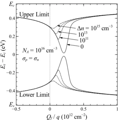
Figure 2.2: Bandgap energy range over which interface state recombination is greater than 90 % of the midgap value, as a function of insulator fixed charge Qf and with bulk excess carrier concentration ∆n as a parameter. We assume
NA= 1016cm−3 and σp=σn.
The first point to note is thatp1 and n1 may frequently be neglected for
inter-face states not very close to the band edge, since they are insignificant compared to either ps orns. This will be the case when either 1) the excess carrier concen-tration ∆n is large, or 2) the surface is in strong accumulation or inversion, such that ps orns is large, regardless of ∆n.
Illustrating this case, Fig. 2.2 shows the bandgap energy range over which interface state recombination efficiency is greater than 90 % of its midgap value, as a function of surface charge and of excess carrier concentration. A bulk acceptor concentration NA= 1016cm−3 and equal capture cross-sections for electrons and holes are assumed (the effect of increasing dopant concentration is to stretch out the curves on theQf/qaxis). When the surface is in depletion, the recombination efficiency of interface states not near midgap is strongly reduced due to competing re-emission of trapped carriers. However, this effect is substantially suppressed when the bulk excess carrier concentration is significant, as under illumination. In accumulation or strong inversion, emission processes are important only for states located near the band edges, regardless of bulk injection.
For the case shown in Fig. 2.2, interface states in the middle 0.7 eV or more of the bandgap contribute equally to recombination for Qf/q >2.5×1011cm−2 or
2.5. Surface recombination 21
charge magnitudes are significantly smaller than those typically encountered at silicon–dielectric interfaces, even in the case of SiO2, which is usually considered to possess a rather low charge. Additionally, interface states located closer to the band edges are generally found to possess rather low capture cross-sections [8], so that they are unimportant for recombination regardless of band-bending. Con-sequently, the neglect of p1 and n1 is frequently justified in determining surface
recombination.
Secondly, in many cases of interest the concentration of one or other carrier will be dominant at the surface, such that recombination is limited by the rate of minority carrier capture. Taking the case of a strongly p-type surface (cpps
cnns), and neglectingp1 and n1 for the reasons described above, Equation (2.18)
reduces to
Us =
psns−n2i
ps
Z Ec
Ev
DitcndE (2.20)
The integral in (2.20) now contains all the terms relating to the interface state properties, and no others. It therefore encapsulates the chemical passivation of the interface. Noting that the integral has units of velocity, we may define a fundamental surface recombination velocity of electrons Sn0, given by
Sn0 =
Z Ec
Ev
DitcndE . (2.21)
The conditions relating to Equation (2.20) will hold for all p-type surfaces and most undiffused n-type surfaces passivated by a negatively charged dielectric such as Al2O3. An analogous expression for Us in terms of Sp0 may be derived
for strongly n-type surfaces.
Sef f and J0s
Because the surface carrier concentrationspsandns are generally not known, it is common to describe surface recombination in terms of an effective surface recom-bination velocitySef f, defined with respect to the excess (non-equilibrium) carrier concentration ∆nd at the edge of the quasi-neutral region of the semiconductor,
Sef f ≡
Us ∆nd
. (2.22)
From (2.20)–(2.22), Sef f is related toSn0 via
Sef f =Sn0
psns−n2i
ps∆nd
≈Sn0
ns ∆nd
where the latter expression applies when the surface carrier concentration is far from thermal equilibrium (psns n2i). For surfaces not in inversion, i.e. where the surface minority carriers are the same as those in the near-surface quasi-neutral region, we can make the further substitution ∆nd ≈ nd. Note that it is not necessary to include bandgap narrowing in the calculation of ns and ps in (2.23), so long as this effect is approximately constant over the surface space-charge profile induced by Qf.
Making the substitutionpsns ≈(Ns+ ∆nd)∆nd, (2.23) can be rewritten as
Sef f =Sn0
(Ns+ ∆nd)
ps
, (2.24)
where we have assumed that the surface dopant concentrationNs is equal to that at the edge of the quasi-neutral region. Using the approximate expression for ps provided by Equation (2.12) when Qf is large and the carrier concentrations are nondegenerate, this becomes
Sef f =Sn0
2kT s
Q2
s
(Ns+ ∆nd). (2.25)
Equation (2.25) shows that Sef f in this case is dependent on both the dopant concentration and the injection level. This limits the usefulness of Sef f as a means of characterising surface recombination, as discussed by [113].
As an alternative to Sef f, we may instead describe surface recombination in terms of the surface saturation current density J0s, defined by [113]
J0s=qUs
psns−n2i
n2
i
−1
. (2.26)
Combining (2.20), (2.21), and (2.26), we find, for a strongly p-type surface,
J0s=qSn0p−s1n
2
i . (2.27)
Again using the high-charge, nondegenerate approximation forpsgiven by (2.12), we obtain
J0s =qSn0
2kT s
Q2
s
n2i . (2.28)
2.6. Relationship to experimental parameters 23
2.6
Relationship to experimental parameters
Generally, one does not measure surface recombination directly, but rather the effective excess minority carrier lifetimeτef f, typically as a function of the average excess carrier concentration ∆n. τef f is defined by
τef f ≡ ∆n Utotal
, (2.29)
whereUtotalis the total volumetric recombination rate due to all mechanisms, both in the bulk and at the surface. τef f can therefore be expressed as the parallel combination of the carrier lifetimes due these various recombination processes. We consider the case of a uniformly doped, undiffused sample. Then
τef f−1 =τint−1+τSRH−1 +τs−1, (2.30) where τint is the intrinsic bulk lifetime due to radiative and Auger recombina-tion [31], τSRH is the extrinsic bulk lifetime due to SRH recombination through bulk defects, and τs is the carrier lifetime due to surface recombination. For a symmetrically passivated, undiffused wafer, τs is related to Us by
τs =
W
2 ∆n
Us
. (2.31)
whereW is the wafer thickness, andUs refers to the value at each surface. Equa-tion (2.31) assumes that ∆nis uniform throughout the width of the wafer, which may not hold if the generation profile is significantly nonuniform, or surface re-combination is very large.
Combining Equations (2.22), (2.30), and (2.31), and using the fact that for undiffused surfaces ∆nd = ∆n, we arrive at the following expression for Sef f in terms of τef f:
Sef f =
W
2
1
τef f
− 1
τint
− 1
τSRH
(2.32)
Sef f determined from (2.32) is commonly used to characterise surface recombina-tion at undiffused surfaces, and will be used extensively in the following chapters for this purpose. Since τSRH is generally unknown, it is usually assumed that
τSRH−1 = 0, so that the calculated Sef f represents an upper limit.
For diffused surfaces, it is more common to describe the recombination rate in terms of a saturation current density J0, analogous to the surface saturation
in the heavily doped diffusion in addition to SRH recombination at the surface. Assuming ∆nni, we may write [116]:
J0 =qn2i(Nb+ ∆n)−1
W
2
1
τef f
− 1 τint − 1 τSRH , (2.33)
where Nb is the bulk dopant concentration. The use of J0 rather than Sef f has the advantage that J0 is independent of ∆n at such surfaces, so long as
recombination at the surface itself remains limited by minority carrier capture [116]. Equation (2.33) may be used directly to calculate J0 fromτef f for a given ∆n. However, this has the disadvantage that the extracted J0 includes τSRH, since this is generally not known independently. Instead, assuming that J0 is
independent of ∆n, we may take the derivative of (2.33) with respect to ∆n, leading to
J0 =qn2i
W
2
d d∆n
1
τef f
− 1 τint − 1 τSRH . (2.34)
J0 may thus be determined from the linear slope of τef f−1 − τ
−1
int vs ∆n [116]. This has the advantage that if the bulk is in high injection (∆n Nb), τSRH is independent of ∆n, so that the extractedJ0 is unaffected by error due to extrinsic
bulk recombination, even if such recombination is significant. Such conditions are readily obtained using high resistivity (lightly doped) substrates.
Although usually applied to characterise recombination at diffused surfaces,J0
determined from Equations (2.33) or (2.34) is also of use to characterise undiffused surfaces where surface recombination is dominated by minority carrier capture. For an undiffused wafer with uniform doping and injection, psns= (Nb+ ∆n)∆n, and therefore J0 = J0s. Thus, when the conditions relating to (2.20) apply, J0
derived from Equations (2.33) or (2.34) provides an injection-independent means of characterising surface recombination at undiffused surfaces.
Note that the measured quantity in all cases is, in fact,J0/n2i, which is also the quantity relevant to recombination, and is essentially independent of temperature. Consequently, the choice of ni used to extract J0 is arbitrary. We present results
in terms ofJ0 rather thanJ0/n2i only because this is the convention. It is however a trivial matter to apply a different value of ni in order to make the J0 values
comparable with those quoted by other authors using different values of ni. In all cases in this work we use ni given by [107] at 300 K (9.7×109cm−3).
Finally, we note that by comparison of (2.32) and (2.33),Sef f is related toJ0
by
Sef f =J0
Nb+ ∆n
qn2
i
2.6. Relationship to experimental parameters 25
Chapter 3
Al
2
O
3
Deposition and
Characterisation
Toward the effecting of works, all that man can do is to put together or put asunder natural bodies. The rest is done by nature working within.
— Francis Bacon
The New Organion
In this chapter we describe the experimental techniques used in this work to deposit and characterise the Al2O3 films. Deposition of almost all Al2O3 films examined in this work was performed by the APCVD method, except in a few cases where Al2O3 was deposited by ALD. Therefore we begin in Section 3.1 with a detailed description of the APCVD deposition technique and the APCVD system used to deposit the Al2O3 passivation layers, including a discussion of the various options for the chemical precursor. The details of the more established ALD process are given briefly in Section 3.2, where we also describe the general procedures used for sample preparation. Finally, in Section 3.3 we describe the principal experimental techniques employed to characterise the samples.
3.1
Al
2O
3deposition by APCVD
APCVD is a versatile process that can be used to deposit many different mate-rials. As a chemical vapour deposition (CVD) method, deposition is based on the chemical reaction of one or more precursor molecules in the vapour phase.
Al N2 H2O
N2
H2O
Exhaust Exhaust
Mixing + Deposition
Substrate Transport
Heating
Figure 3.1: Schematic illustration of the APCVD Al2O3 deposition system used in this work, showing the configuration of the various input gas flows (Al precursor, H2O or O2 reactant, and separator N2).
The deposition reaction occurs at the substrate surface, or nearby, and generally requires an external source of energy. For APCVD that energy is purely thermal, coming from the temperature of the substrate (PECVD, on the other hand, sup-plements this thermal energy with energy from an ionised plasma). Importantly, the entire process takes place at atmospheric pressure.
The deposition reaction may be based on one or more of several mechanisms, including pyrolysis (thermal dissociation), hydrolysis (reaction with water), ox-idation, nitrox-idation, or reduction. The reaction may involve a single, or two or more reactant species (common secondary species include H2O, O2, CO2, and NH3). The primary reactant, or precursor, is often a metal-organic molecule. In this case the process may also be referred to as metal-organic chemical vapour deposition (MOCVD).
![Figure 1.1: Energy conversion efficiency of a typical high-efficiency Czochralskia conventional Al-alloyed “back surface field” (BSF) [1]–[7] are shown (literaturevalues are adjusted to the relevant substrate dopant concentration according toand atmospheric pre](https://thumb-us.123doks.com/thumbv2/123dok_us/8116241.238271/24.595.178.376.107.304/conversion-eciency-eciency-czochralskia-conventional-literaturevalues-concentration-atmospheric.webp)


![Figure 3.2: Vapour pressure data taken from the literature [117], [121]–[128] forselected Al precursors.](https://thumb-us.123doks.com/thumbv2/123dok_us/8116241.238271/54.595.173.376.100.307/figure-vapour-pressure-data-taken-literature-forselected-precursors.webp)