International Journal of Innovative Technology and Exploring Engineering (IJITEE) ISSN: 2278-3075, Volume-8 Issue-8S2, June 2019
Abstract: It is now very common to have SoC-powered IoT devices due to their low power consumption. This paper proposes a low-cost SoC implementation of the AES algorithm for resource constrained devices. The AES cryptographic module is based on a four-stage sub-pipelined architecture for encryption/decryption of all the standard key sizes (128, 192 and 256 bits) of AES. An on-the-fly key generator was implemented, making use of a single 32-bit XOR together with an 8-deep shift register as the main components to compute round keys. The RTL of the architecture was designed using Verilog HDL and simulated with ModelSim. Also, a parallel and resource-shared MixColumn/Inverse MixColumn module was implemented to ensure a short critical path of the design. Synthesis of the proposed AES hardware implementation was done with Synopsys Design Compiler using the 180nm TSMC cell library. AES has been in use since the year 2001, when it replaced the DES algorithm. Most implementations in the past have been done in the software domain. However, it was discovered that the hardware implementation of AES is far better than its software counterpart for reasons of robustness and speed. Also, by using a four-stage pipeline, the proposed architecture is able to achieve a small area while providing a high throughput needed for the fast propagation of data. The proposed architecture achieved a low area of 16.1K NAND2 gate equivalent. A memory unit of size, 9.152KB was implemented to cater for the S-Box/Inverse S-Box modules. The maximum frequency of the design was 621.12MHz, which resulted in average throughputs of 7.15Gbps, 6.06Gbps and 5.26Gbps for 128-bit, 192-bit and 256-bit key lengths respectively. The proposed SoC–based AES cryptographic system can be applied to resource constrained devices that require high-performance as well as robust security, such as IoT devices.
Index Terms: System-on-a-Chip, RISC-V, On-the-fly key generation, Encryption, Decryption, Sub-pipelined architecture.
I. INTRODUCTION
In order to facilitate daily transactions, IoT technology was birthed. This saw the manufacture of next generation resource-constrained devices that required less power, were small and served several purposes in sectors such as health, sports and education. However, these devices susceptible to attacks from unwarranted users, since they operate over public networks. With the rapid growth of the internet, the need to provide robust encryption for these SoC-powered devices has not been more pertinent. In order to resolve this
Revised Manuscript Received on May 22, 2019.
Alexander Owusu-Ansah Antwi, Department of Information and Communication Engineering, Hanbat National University, Daejeon, South Korea.
Kwangki Ryoo, Department of Information and Communication Engineering, Hanbat National University, Daejeon, South Korea.
situation and curtail the activities of malicious hackers, a strong encryption system has to be implemented on the chip. In order to be able to provide encryption, a sound understanding of cryptography required. Cryptography is usually used interchangeably with encryption. However, encryption is a term given to the mere modification of an intelligible piece of data into one that cannot be comprehended. Cryptography on the other hand involves the application of complex mathematics in order to design strong encryption techniques to protect private data. Encryption finds applications in smart cards, mobile networks, e-commerce and automated teller machines (ATM). In order to prove the robustness of an encryption algorithm, four main areas are considered, to wit confidentiality, authenticity, non-repudiation and integrity [1]. Cryptography can be classified into two main branches, which are, private key (symmetric) and public key (asymmetric) cryptography. With symmetric cryptography, a single key, known to both sender and receiver of the data is used in the encryption and decryption of the data. This requires that a key exchange over a secure network be in place prior to the transaction. With asymmetric cryptography two different keys are employed each for encryption and decryption of data. The sender encrypts with his key and sends the message. When the receiver receives the message, he uses his key to decrypt the data. The advantage of this using this approach is that the two parties can be unknown entities who have no prior information of each other. However, due to the more computationally intensive nature of these algorithms, they are seldom used to encrypt large data or frequently changing data. Commonly, they are used to create and exchange the key to be used by symmetric encryption. The Rivest-Shamir-Adleman (RSA) and the Elliptic Curve Cryptography (ECC) are examples of asymmetric cryptographic systems. Examples of the symmetric algorithms are the Data Encryption Standard (DES) and the Advance Encryption Standard (AES). Since the year 2001, the AES has been in use, having replaced the DES, which was the main encryption algorithm used from 1975. Since then, the AES algorithm has been adopted for use in many systems such as smart cards, mobile phones, USB keys and banking systems [2]. The AES algorithm was designed to be implemented in both software and hardware. However, several concerns have arisen over time about the security of software implementations of encryption algorithms. To say
the least, software
implementations are
considered non secure since can be easily exploited
A System-on-a-Chip Design of the AES
Cryptographic System
remotely by an intruder. On the other hand, with hardware implementations, the intruder will need physical access to the device before he can do some serious damage to the system [3]–[5]. This is the reason why there have been various researches into hardware implementations of AES since its standardization. In these, researchers’ main focus has been on optimization for low area and throughput and power.
Various techniques are utilized for various optimization requirements, and these depend on the availability of resources as well as frequency prerequisites. For high-speed architectures, designers can decide to use the loop-unrolled architecture as the basic structure, while the rolled (basic iterative) architecture is used when a low area design is desired. Usually, these basic structures are used in tandem with techniques such as pipelining and resource sharing. For high-speed implementations, the loop unrolled architecture and pipelining are used. If the intent is to achieve a small hardware footprint, the rolled iterative architecture is employed [6]. Many implementations of the loop unrolled architecture with and without pipelining have been carried out in the past that have yielded designs with impressively high throughputs but with huge number of gates [7]. Many other researchers have used methods that have helped to the reduce area of their implementations of AES. One such method has been to implement the S-Box module of AES based on composite combinational logic. However, although this method serves to drastically reduce the area of the designs [8], it increases the critical path and throttles the maximum frequency. Another method used in area reduction is to implement the key generation unit as an on-the-fly unit. By so doing, we avoid using additional memory to store the initially generated keys [9]. The following shows the works of some of the researchers referenced in this paper. The authors in [10] proposed three different SoC-based implementations of AES. For their area reduction techniques, they used the compact composite combinational logic for the S-Box implementation. Also, in [2], the authors adopted the iterative structure so as to realize a small area. In addition to that, the key generation was implemented as an on-the-fly circuit. The use of memories was avoided by implementing the SubByte and Inverse SubByte as a shared logic unit based on composite field arithmetic. In so doing, the achieved area was 19.476K equivalent NAND2 gates and a frequency of 100MHz. The architecture used in [11] was the rolled architecture, without pipelining. All the keys were expanded once and kept in memory for later use during encryption/decryption. The SubByte unit was designed as a LUT-based structure. The resulting area was 58,445 gates, with a frequency of 125MHz.
This paper proposes a low Cost SoC implementation of the AES cryptographic system. In order to reduce the area and increase the throughput, the iterative architecture was combined with a four-stage pipelined structure. The key generator was implemented as an on-the-fly unit while the SubByte was implemented as an LUT-based unit. In the rest of this paper, Section II gives a brief background on SoC and AES cryptosystem. This is followed by the proposed
architecture of the SoC and the implementation results and finally the conclusion.
II. THEORETICAL BACKGROUND
A System-on-a-Chip is a single integrated-circuit that contains all the necessary circuits and parts such as an analog-to-digital converter, memory, logic control units, I/O interfaces, and performs digital, mixed-signal as well as analog functions. It is common to find in a SoC, at least one processor, memories, and system interconnects designed and verified for an application domain. The on-chip components could also include an operating system or an application tailored for a specific task, firmware, analog circuits, and accelerators. Not all SoCs have just one processor. SoCs, such as those found in smartphones need to support internet access, audio I/O functions, as well as multimedia functionalities for video communications. As such, it is not uncommon to find SoCs with a number of processors connected to one or more memory and peripheral units [12]. In a SoC, it is important for all the connected IPs and peripherals to communicate smoothly with the processor at their own speed. In order to ensure this, all the IPs should be fitted with a bus interface to ensure smooth interoperability.
A. The Standard AES Algorithm
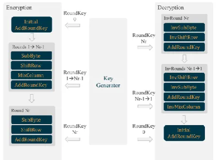
The standard AES is a block cipher with block size of 128 bits and a key (128, 192 or 256 bits in size) that is used in encryption and decryption. Both encryption and decryption are performed in a number of iterations over four main round functions. The four functions iterated over in the encryption process are the SubByte, ShiftRow, MixColumn and AddRoundKey functions. The number of iterations performed are dependent on the size of the key being used. Fig. 1 shows the structure of the standard AES encryption/decryption structure.
Fig. 1. Standard AES Algorithm Structure
The plaintext to be encrypted can be visualized as a 4x4 matrix, known as the state. Each index of the matrix contains a byte of the plain text from top to bottom and left to right [13]. At the end of the total number of rounds, the state is
transformed into a
[image:2.595.319.543.493.658.2]International Journal of Innovative Technology and Exploring Engineering (IJITEE) ISSN: 2278-3075, Volume-8 Issue-8S2, June 2019
the SubByte/Inverse SubByte transformation is to add non-linearity to the state by substituting each byte with its bijective mapping. Usually this is done by means of a look-up-table, but it can also be done by means of combinational circuits in the hardware domain if area reduction is the sole purpose. The ShiftRow/Inverse ShiftRow adds diffusion to the state matrix. This ensures that a single character change at the input will affect many characters at the output. The first row is always unchanged not changed. However, the second to the fourth rows are shifted cyclically by 1 byte to 3 bytes respectively in increments of a byte. For the ShiftRow function, the shift is done in the left direction, whiles it is done to the right direction for the Inverse ShiftRow. MixColumn /Inverse MixColumn is also a diffusion function whose operations mainly consist of multiplication of the columns of the state with fixed matrices [14]. There are two matrices in all, one used for MixColumn as shown in (1), and the other used for decryption, as shown in (2).
0 0
1 1
2 2
3 3
02
03
01
01
01 02
03
01
01
01 02
03
03
01
01 02
b
a
b
a
b
a
b
a
(1)
0 0
1 1
2 2
3 3
0
0
0
09
09
0
0
0
0
09
0
0
0
0
09
0
b
E
B
D
a
b
E
B
D
a
b
D
E
B
a
b
B
D
E
a
(2)
In the last round of encryption as well as in the first-round decryption, MixColumn and Inverse MixColumn are respectively omitted. In the AddRoundKey function, the state is XORed with the round key computed by the key generator. There is no inverse function for this function as the XOR function is its own inverse. Initially, the key is added to the state in what is shown as Initial AddRoundKey operation in Fig. 1 above. This operation is performed just once in the encryption or decryption of a single 128-bit block of plaintext or ciphertext. The SubByte, ShiftRow and MixColumn and AddRoundKey operations follow on, in operating on the state.
B. Key Schedule
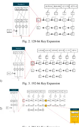
The function of the AES key generator is to take as input, the cipher key and from it, derive round keys that correspond to the rounds of encryption/decryption [15]. The total number of rounds in encryption/decryption is dependent on the size of the key. In order to understand the key generation, we need to picture the input key as well as the sub-keys as 32-bit word divisions. As such, the 128-bit key will have 4 words, 192-bit key will have 6 words and the 256-bit key will have 8 words. The words are arranged, in each iteration, from the most significant word to the least significant word.
The divisions and computation of sub-keys are illustrated in Fig. 2, Fig 3, and Fig 4.
[image:3.595.292.550.80.491.2]Fig. 2. 128-bit Key Expansion
Fig. 3. 192-bit Key Expansion
Fig. 4. 256-bit Key Expansion
Each line represents an iteration of the key generation with the words labelled from W4i to W4i-1 where i =1,2…Nk. Each
W4i is computed as shown in (3).
4i 4(i 1)
(
4i 1)
W
W
G W
(3)Nk is calculated as shown in (4):
(
Total
_
Number of
_
_
word
4) / 4
(4)The function, G(x) is a non-linear function comprising of a 32-bit SubByte module, RotWord function and a round constant addition routine. The word rotation function is a cyclic shift of the 32-bit word to the left by one byte. The computation of the other words is as shown in (5).
4i j 4i j 1) (i 1),j
;
1, 2,...
W
W
W
j
Nb
(5) [image:3.595.50.219.304.468.2]bits. For AES-256, there is an additional function, H(x) which applies the S-Box to all four input bytes of the rightmost word. The total number of computed sub-keys and round keys vary for each key length. Table 1 summarizes the number of round keys and sub-keys.
Table 1. Characteristics of AES Standard Key Lengths
AES Type Rounds Iteration s
Word per Iteration
Word Range
AES-128 10 11 4 W0-43
AES-192 12 8 6 W0-51
AES-256 14 7 8 W0-63
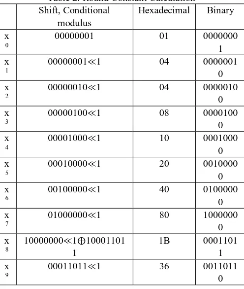
[image:4.595.37.298.134.206.2]The round constant addition adds an 8-bit constant (unique for each iteration) to the most significant byte after word rotation. Its purpose is to eliminate any symmetry or similarity between the generated round keys [16]. The addition is shown in Table 2.
Table 2. Round Constant Calculation Shift, Conditional
modulus
Hexadecimal Binary
x 0
00000001 01 0000000
1 x
1
00000001≪1 04 0000001
0 x
2
00000010≪1 04 0000010
0 x
3
00000100≪1 08 0000100
0 x
4
00001000≪1 10 0001000
0 x
5
00010000≪1 20 0010000
0 x
6
00100000≪1 40 0100000
0 x
7
01000000≪1 80 1000000
0 x
8
10000000≪1⨁10001101 1
1B 0001101
1 x
9
00011011≪1 36 0011011
0
III. PROPOSED SYSTEM-ON-A-CHIP DESIGN
The proposed SoC architecture works with
Von-Neumann’s stored program concept. The program, written in C, is compiled and stored in memory, to be fetched, decoded and executed by the RISC-V processor. The full SoC structure is shown in Fig 5.
Fig. 5. Proposed SoC Crypto-System
A. Software Test Program
[image:4.595.45.293.302.595.2]International Journal of Innovative Technology and Exploring Engineering (IJITEE) ISSN: 2278-3075, Volume-8 Issue-8S2, June 2019
Fig. 6. Software Routine for Encryption/Decryption
B. Proposed AES Hardware Architecture
[image:5.595.80.260.49.291.2]In our proposed architecture, each of the four sub-round transformations is performed in one clock cycle. The proposed architecture for encryption and decryption is shown in Fig 6.
Fig. 6. Proposed AES Hardware Architecture
The proposed architecture iterates over the modules shown, in order to perform encryption/decryption for all the standard key sizes. There is an addition of one clock cycle for the decryption process. This is because for encryption, the AddRoundKey is performed in the fourth cycle in the pipeline which coincides with the cycle in which the round key computation is finished. However, for decryption, the AddRoundKey is the third to be executed, which means the round key will not be available at in that cycle. For this reason, a single cycle delay is inserted so as to match the output of the round key output with the of the AddRoundKey routine.
C. Proposed MixCol Unit
The proposed MixCol is a shared module for both MixColumn and its inverse. It is worth noting that multiplication in hardware can be implemented as left shift operations. In GF(28), however, a conditional modulo is
performed on the left-shifted result. For instance, Multiplication by 0x02 in GF(28) is basically a shift operation modulo a field polynomial, 0x011B. The addition operation is a modulo-arithmetic carried out in GF(28) [17]. The multiplication of the four-byte word by the hexadecimal values in the matrices are simplified in Table 3. Also, multiplication by 0x02 is shown in (6) below.
02
A
i(
A
i
1)
(1
B A
i[7])
(6)Table 3. Multiplication in GF (28) 03 · Ai (Ai · 02) + Ai
04 · Ai 02 · (Ai · 02) 08 · Ai 02 · (Ai · 04) 09 · Ai (Ai · 08) + Ai 0B · Ai (Ai · 09) + (Ai · 02) 0D · Ai (Ai · 09) + (Ai · 04)
0E · Ai (Ai · 08) + (Ai · 04) + (Ai · 02)
[image:5.595.331.522.188.289.2]The architecture for the proposed MixCol module is shown in Fig. 7 and Fig. 8. In order not to make the already cluttered diagram messier than it already is, the figures have been divided into two: one with MixColumn configuration, as shown in Fig. 7 and the other with Inverse MixColumn configuration as shown in Fig. 8. The two figures however, are the same module.
Fig. 7. MixCol: Encryption Configuration
Fig. 8. MixCol: Decryption Configuration
Each MixCol module consists further of four separate ComMult units, which carry
[image:5.595.56.291.386.554.2] [image:5.595.323.533.402.539.2]vector. In order to perform a one-time computation on the state matrix, four separate blocks were created, thereby trading off area for a low critical path. For the encryption configuration, each byte gets multiplied by 0x01, 0x02, and 0x03. And for the decryption configuration, with 0x09, 0x0B, 0x0D and 0x0E. The results are then XORed together by four XOR units to give a 32-bit output.
D. The ComMult Module
[image:6.595.321.539.230.311.2]This module is constructed by using Mult_02 as a basic block. The main computation of Mult_02 is to multiply an 8-bit vector by 0x02, and this can be done as shown in equation (3) above. To compute Ai2, we use the output from the first Mult_02 unit. For Ai4 or Ai8, we use the outputs from the second or the third Mult_02 module respectively. In order to obtain the productAiB, we need to XOR the outputs of the results from 0x08, 0x02 and 0x01. The other combinations will also give the correct answer, but will cost more in terms of critical path and gate count. The ComMult computes products as shown in Fig. 9.
Fig. 9. ComMult Hardware Structure
E. Proposed Key Generator
[image:6.595.68.282.311.465.2]In order to totally remove the additional cost in area incurred by using memory units to store the keys, the proposed key generator computes each round key on-the-fly key. The architecture of the proposed module is shown in Fig. 10.
Fig. 10. Proposed Key Generator Hardware
The SRRC unit consists of an S-Box unit, RotWord unit, which rotates the word by a byte, and AddRoundConst unit, which adds an 8-bit round constant, RCON to the rotated word. MD is used to select between G(x) and H(x). RKEY is the output round key, while LW is least significant word
W4i-1. A multiplexor is used to select between the SRRC output and LW as one of the inputs of the XOR gate. When
[image:6.595.328.531.510.708.2]the cipher key arrives at the input of the key generator, it is copied into the shift register. At the start of key generation, the relevant registers are shifted to compute the round key. Since the encryption/decryption routines require four cycles per round, in each cycle of the key generation, a 32-bit word is shifted into the output register and then to RKEY. This makes it unnecessary to use more than 1 XOR to compute the round keys. Also, since the proposed architecture uses a shift register instead of a finite state machine to determine the 32-bit word for each cycle, the area, as well as the critical path is reduced. The number of registers that are used in storing the sub-keys is dependent on the key length. Fig. 11 shows the shifting mechanism for AES-128.
Fig. 11. Shifting for 128-bit Key Generation
As shown, the data stored in each register is shifted upwards in every cycle. After four cycles, the key is fetched from the appropriate position of the shift-register and sent to the AddRoundKey module. For AES-128, only the top four registers are used. The value for W10 is calculated prior to the start of the key generation. At the positive edge of the clock, after the assertion of the Start signal, the output of the XOR is stored at the bottom of the active part of the shift-register. In the next cycle, W01 is shifted out of the shift-register. The computed value, W11 is then stored in the bottom (active) part of the shift-register. At the end of four cycles, the round key is {W10, W11, W12, W13}. Fig. 12 shows the shifting mechanism for AES-192.
Fig. 12. Shifting for 192-bit Key Generation
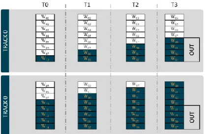
For AES-192, one
[image:6.595.51.294.563.678.2]International Journal of Innovative Technology and Exploring Engineering (IJITEE) ISSN: 2278-3075, Volume-8 Issue-8S2, June 2019
[image:7.595.305.554.49.87.2]key selection, to be computed in the next iteration. It therefore follows that two iterations are required to be able to compute complete round keys in the AES-192 mode. These iterations yield 3 different round keys. Instead of viewing the computations in terms of iterations, we now see them as tracks, whereby a round key is computed in every TRACK iteration. The TRACK determines the values of EN and MD. Below, the shifting mechanism for AES-256 has been presented in Fig. 13.
Fig. 13. Shifting for 256-bit Key Generation
In AES-256, one sub-key is used to generate two round keys. Hence, we need to group the computations into tracks as well. The round key output in TRACK0 is {W10, W11, W12,
W13} and that for TRACK1 is {W14, W15, W16, W17}.
IV. IMPLEMENTATION RESULTS
As is characteristic of iterative designs, this work focused on gaining a small hardware area and high throughput. Table 4 shows a comparison of our results with similar architectures. By using a rolled architecture coupled with a composite logic-based SubByte, the authors in [2] were able to come by a small area of 19.5K gates. However, they were not able to attain a high throughput as compared to the throughput of this proposed architecture. Also, although in [9], the authors used a combinational circuit in the implementation of S-Box, they were not able to attain a small area as compared to our Proposed_2. By using the proposed key generator, the resulting area was smaller as compared to the other references. It can be seen that the throughput of the proposed design is the highest among the three other references. The results of this and that of the referenced papers have been given in Table 4.
Table 4. Results Comparison for 180nm Process
Metric [2] [11] [9] Proposed 1
Proposed 2 Frequency 100 125 300 300 621.1 Through
put (Gbps)
128-bi t
1.1 6
1.6 3.8 4
3.84 7.15
192-bi t
0.9 9
3.2 3.2 6.06
256-bi t
0.8 5
2.7 4
2.7 5.25
Area (K gates) 19. 5
58. 5
39. 9
37.2 39.49
Memory (KB) - - - 9.2 -
Area with Memory (K gates)
19. 5
58. 5
39. 9
13.8 16.1
From the table, it can be seen that the gate count of the proposed architecture exceeds that of [9] by approximately 40%. Proposed_1 has been presented here to be compared with [9]. They used a three-stage sub-pipelined architecture which is similar to the four-stage pipeline of this paper. Although they used the combinational S-Box, their area was not all that good compared to ours. Our maximum frequency is also twice as theirs.
From the results, it can be concluded that, not only was the area reduced, but the throughput was greatly improved as well. The area of the key generator for [11] and this paper is shown in Table 5.
Table 5. Key Generator Area Comparison at 128MHz
Designs Area (K gates)
[11] 8.853
Proposed_2 7.532
V. CONCLUSION
This paper proposed a SoC-based AES cryptographic system that uses a minimum area and yet provides an adequately high throughput. The SubByte and Inverse SubByte units were implemented with an LUT-based logic which, although has a fixed access and cannot be pipelined, reduces the critical path that would have been caused by the combinational logic-based implementation. Furthermore, a low-critical-path and shared MixColumn/Inverse MixColumn unit was implemented. A proposed common unit, ComMult, which combines the multiplication for both MixColumn and Inverse MixColumn in a compact structure with low critical path. The proposed key generator utilizes one 32-bit XOR in the computation of the round keys. In every cycle, a 32-bit word is computed and appended to a shift register. The use of the shift registers provided a smaller logic than would be required for say, a finite state register. The proposed AES crypto core yielded a maximum frequency of 621.12MHz which translates to an average throughput of 7.15Gbps, 6.06Gbps and 5.25Gbps for AES-128, AES-192 and AES-256 respectively. The total area was 16.1K gates with 9.216KB memory.
REFERENCES
1. S. William, Cryptography and Network Security: Principles and Practices. Pearson Education Limited, 2013, p. 42.
2. Q. Cao and S. Li, “A High-Throughput Cost-Effective ASIC Implementation of the AES Algorithm,” IEEE 8th International Conference on ASIC China, 2009, pp. 805–808.
3. Infosecurity Group. (2018, Aug 31). Tales from the Crypt: Hardware vs
Software [Online]. Available:
https://www.infosecurity-magazine.com/magazine-features/tales-crypt-har dware-software
4. K. Gaj and P. Chodowiec, Cryptographic Engineering: FPGA and ASIC Implementations of AES. Springer US, 2009, p. 15.
5. P. Saravanan, R. N. Devi, G. Swathi, and P. Kalpana, “A High-Throughput ASIC Implementation of
Configurable Advanced
[image:7.595.69.278.179.316.2]Applications, vol. 3. Dec. 2011, pp. 1–6.
6. N. Bhat and V. Shridhar, “FPGA Implementations of Advanced Encryption Standard: a Survey,” International Journal of Advances in Engineering & Technology, vol. 3. May. 2012, pp. 265–285.
7. R. R. Farashahi, B. Rashidi, and S. M. Sayedi, “FPGA Based Fast and High-Throughput 2-Slow Retiming 128-bit AES Encryption Algorithm,”
Microelectronics Journal, vol. 45. May. 2014, pp. 1014–1025. 8. H. Shaji and P. L. Bonifus, “Design of AES Architecture with Area and
Speed Tradeoff,” Procedia Technology, vol. 24. Jul. 2016, pp. 1135–1140.
9. H. Li, “Efficient and Flexible Architecture for AES,” IEE Proceedings - Circuits, Devices and Systems, vol. 153. Dec. 2006, pp. 553–538. 10.Z. Xie, J. Han, J. Yang, L. Zhou, and X. Zeng, “A Low-Cost SoC
Implementation of AES Algorithm for Bio-Signals,” IEEE 11th International Conference on ASIC China, 2015, pp. 1–4.
11.P. V. S. Shastry, A. Kulkarni, and M. S. Sutaone, “ASIC Implementation of AES,” Annual IEEE India Conference India, 2012, pp. 1255–1259. 12.M. J. Flynn and W. Luk, Computer System Design: System-on-Chip. John
Wiley & Son Inc., 2011, p. 24.
13.National Institute of Standards and Technology. (2018, Aug 31). Advanced Encryption Standard (AES) [Online]. Available: http://csrc.nist.gov/publications/fips, 2001.
14.F. Hossain, Design of a High-Speed AES Crypto Processor ASIC.
Lambart Academic Publishing Company, 2013, p. 37.
15.I. M. Hammad. (2018, Aug 31). Efficient Hardware Implementations for the Advanced Encryption Standard (AES) Algorithm [master’s thesis]. Dalhousie University, Halifax, 2010, p. 103.
16.I. Saberi, B. Shojaie, and M. Salleh, “Enhanced Key Expansion for AES-256 by using Even-Odd method,” International Conference on Research and Innovation in Information System Malaysia, 2011, pp. 1–5. 17.C. Paar and J. Pelzl, Understanding Cryptography: A Textbook for
Student and Practitioners. Springer-Verlag, 2010, p. 102.
AUTHORSPROFILE
Alexander Owusu-Ansah Antwi was awarded a BSc. Degree in Computer
Engineering from Kwame Nkrumah
University of Science and Technology, Ghana, in 2014 and an M.Eng. Degree in Information and communication engineering from Hanbat National University, South Korea in 2019. His research interests include SoC Design and Verification Platforms, Lightweight Cryptography, and SoC Design for Security.