Small-Scale Liquid-State Dynamics in Nanometer Size
Devices
Thesis by
David Nicholas Barsic
In Partial Fulfillment of the Requirements
for the Degree of
Doctor of Philosophy
California Institute of Technology
Pasadena, California
2004
c
2004 David Nicholas Barsic
Acknowledgements
I would like to thank Professor Axel Scherer for his continual guidance, support, and encouragement
throughout this work. Also appropriate are thanks to Caltech for providing a stimulating learning
environment and excellent facilities, without which this research would not have been possible. To
my undergraduate advisers: Helen Na, Peter Schwartz, Norbert Malik, John Robinson, and Winston
Chan whose guidance, advice, and support were key to my important career choices.
I would like to thank all of the members of the Nanofabrication lab: Mark Adams, Tom
Baehr-Jones Mladen Barbic, Chuan Chen Cheng, Hou-Pou Chou, Guy Derose, Oliver Dial, Theodore
Doll, Teresa Emery, Kate Finnigan, Michael Hochberg, Ali Husain, Reynold Johnson, Thomas
Krauss, Yves Lassailly, Marko Loncar, George Maltezos, Brett Maune, Marlene Moncada, Terrell
Neal, Koichi Okamoto, Oscar Painter, J¨org Schilling, Michelle Vine, Jelena Vucovi´c, Chris Walker,
Jeremy Witzens, Joyce Wong, Tomoyuki Yoshie, Zhaoyu Zhang. All of you have made my time at
Caltech enjoyable. I am honored to have had the chance to work with and learn from all of you.
I am very much in debt to Bill Bing, Brad Jensen, and Mark Weber who helped me to get back
in the groove at times when I was a little off key and behind the beat. To my adopted family
in California: Jason, Sabrina, and Alexandra Feldman, thank you for your encouragement and
hospitality.
To all of my heroes and role models: Jeff Bergthorson, Will Green, Victor Hristov, Ali
Hu-sain, Michael Johnson, Reynold Johnson, Conrad Josias, Reginald Lee, Guillaume Lessard, Shelly
Levy-Tzedek, Scott Mehrens, Nick Papadakis, Clara Reis, Miguel Remondes, Joseph Schmidt, Ben
Shapiro, and Danielle Svhela; your steady, unfaltering friendship means the world to me.
Without continual support, encouragement, and love of my family none of this would have been
possible. Thank you Mom, Dad, Mary, Jayson, Paul, Tessa, Sarah, Angie, and Tony for always
Abstract
This dissertation will present research on state-of-the-art micrometer- and nanometer-scale
machin-ing techniques to fabricate fluid channels with integral sensmachin-ing electrodes. The motivation for this
project is to create new instruments for investigating the behavior and properties of particles or
molecules in solution and confined in a fluid channel with cross-sectional dimensions ranging from
less than 50 nanometers to one micron.
The objective of this research is to develop techniques for building fluid analysis systems which
combine fluid channels with sensing electrodes. Design of physical devices and the measurement
cir-cuit are both important steps in accomplishing this task. The design issues necessary for optimizing
these aspects are investigated in detail. The size scale of these systems is at the lower limit
achiev-able with current technology. Such devices require critical dimensions of less than 100 nanometers
in order to perform measurements on small-scale fluid systems. Applications of this type of system
include detection of both the presence and the motion of particles and molecules suspended in the
small volume of fluid confined within the fluid channel. The motion of particles in the fluid channel
is detected by measuring the change in electrode capacitance as particles move past the electrodes.
Typical fluid volumes used in this type of system range from 50 femtoliters (50x10−15l) to less than
one femtoliter.
Accomplishing this task required a careful look at the machining techniques for making
micro-scopic devices. The approach is to use lithographic and circuit manufacturing techniques to make
small fluid channels on either side of which are sets of electrodes. Existing techniques for making
small-scale devices were modified to provide the required performance. In some cases the
Contents
Acknowledgements iv
Abstract v
1 Introduction 1
1.1 Introduction . . . 1
1.2 Previous Work . . . 2
1.3 Nanometer-Scale Fluid Channels . . . 3
1.4 Pumping Fluid in Nanometer Channels . . . 3
1.5 Nanometer-Scale Sensing Electrodes . . . 4
References . . . 6
2 Lithography Techniques for Nanometer Sized Fluid Channels and Electrodes 9 2.1 Introduction . . . 9
2.2 Sub-micron Scale Lithography . . . 9
2.3 Photolithography . . . 10
2.4 Shadow Mask Lithography . . . 12
2.5 Electron-Beam Lithography . . . 17
2.6 Electron Image Projection System . . . 21
2.7 Conclusion . . . 21
References . . . 23
3 Fabrication Procedure for Nanometer-Sized Fluid Channels and Electrodes 25 3.1 Introduction . . . 25
3.2 Thin Film Deposition . . . 25
3.2.1 Thermal Evaporation . . . 25
3.2.3 Sputtering . . . 27
3.3 Etching . . . 28
3.3.1 Reactive Ion Etching . . . 28
3.3.2 Ion-Beam Etching . . . 29
3.3.3 Chemically Assisted Ion-Beam Etching . . . 32
3.4 Surface Cleaning . . . 34
3.4.1 Radio Corproation of America (RCA) Cleaning Process . . . 36
3.5 Conclusion . . . 37
References . . . 38
4 Nanometer Fluid Channels 39 4.1 Introduction . . . 39
4.2 Lithography . . . 40
4.2.1 Electron-Beam Lithography . . . 40
4.3 Etching Nanometer Fluid Channels . . . 42
4.3.1 Transferring the Resist Pattern to the Metal Mask Layer . . . 42
4.3.2 Etching Techniques for Fused Silica Fluid Channels . . . 43
4.3.3 Etching Techniques for Silicon Fluid Channels . . . 45
4.3.4 Etching Techniques for Polymer Channels . . . 45
4.4 Methods of Sealing Nanometer Fluid Channels . . . 50
4.4.1 Surface Preparation . . . 50
4.4.2 Anodic Bonding . . . 52
4.4.3 Fusion Bonding . . . 52
4.4.4 Room Temperature HF Bonding . . . 52
4.5 Imaging Techniques for Fused Silica Fluid Channels . . . 53
4.6 Fluorescent Confocal Microscope Measurements . . . 53
4.7 Conclusion . . . 57
References . . . 58
5 Pumping Liquids at Nanometer-Size Scales 59 5.1 Introduction . . . 59
5.3 Conditions for Electro-Osmotic Flow (EOF)
in Fluid Channels . . . 64
5.3.1 Controlling the Properties of the Electric Double Layer . . . 66
5.3.2 Design of Electro-Osmotic Flow Channels . . . 67
5.3.3 Building the EOF Test Setup . . . 69
5.3.4 Measurement Circuit . . . 70
5.3.5 Experimental Results of the EOF test setup . . . 70
5.4 Conclusion . . . 72
References . . . 74
6 Nanogap Capacitive Sensing Electrodes 78 6.1 Introduction . . . 78
6.2 Nanogap Electrode Overview . . . 78
6.3 Nanogap Electrode Capacitance Calculations . . . 79
6.3.1 Analytic Calculations . . . 79
6.3.2 Finite Element Modeling of the Capacitance Between Two Spheres . . . 81
6.3.3 Finite Element Modeling of the Capacitance Between a Pair of Nanogap Elec-trodes . . . 82
6.3.4 Change in Nanogap Electrode Capacitance in the Presence of a Nano-particle 84 6.4 Nanogap Electrode Design . . . 85
6.5 Conclusion . . . 87
References . . . 88
7 Electrical Measurement 89 7.1 Introduction . . . 89
7.2 Types of Measurement Circuits . . . 89
7.2.1 Charge/Discharge Technique . . . 89
7.2.2 Oscillator Circuit Methods . . . 91
7.2.3 Inductive-Capacitive Resonator Circuit . . . 91
7.2.4 AC Bridge Circuit . . . 92
7.3 Precision Ratio Transformer Balancing of the AC Capacitance Bridge . . . 93
7.4 Capacitance Measurement Circuit Results . . . 96
7.6 Conclusion . . . 100
References . . . 102
8 Conclusions 103
List of Figures
2.1 Screen printing process: a. The screen is attached to a rigid frame and patterned with
pore-blocking paint. b. The screen is held against the work piece. c. Ink is forced
through the pores and onto the surface of the work piece. d. The finished result is a
pattern in the ink. . . 10
2.2 Photolithography process steps: a. Align mask with the photoresist coated substrate. b. Bring the mask and substrate together, and expose the photoresist to ultra violet light through the mask. c. Develop the photoresist to remove exposed areas. d. After developing the substrate is ready for subsequent processing steps. . . 11
2.3 Cross-sectional view of photoresist stripes on a silicon wafer. . . 11
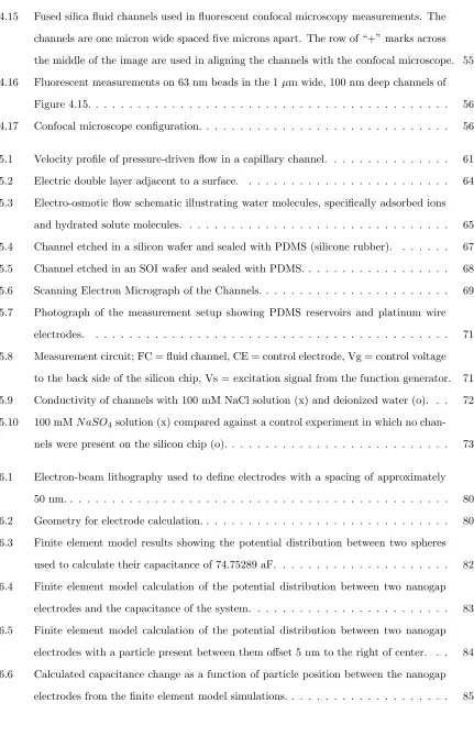
2.4 Shadow mask process: a. Begin with a photoresist feature. b. Evaporate the metal etch mask at an angle Θ from normal. c. Pattern is transferred into the substrate with a directional etch. d. Final result after removal of the etch mask and photoresist. . . . 12
2.5 Cross-section of a fluid channel made with a shadow mask technique. . . 13
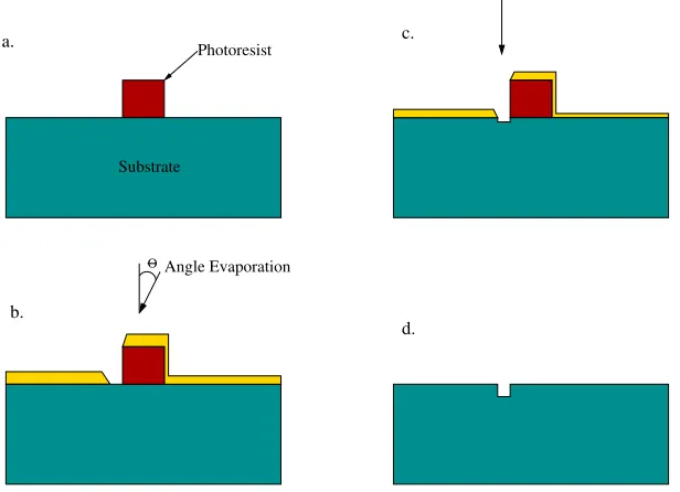
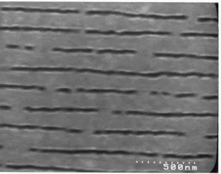
2.6 Line made using shadow mask technique. . . 14
2.7 Undercut etch technique: a. Begin with a photoresist feature on top of a mask material. b. Etch exposed mask areas with an isotropic etch to remove the mask material just under the photoresist edges. c. Deposit a second etch mask layer. The overhanging edge of the photoresist will create a small gap. d. Pattern is transferred into the substrate with a directional etch. . . 15
2.8 Results of the chrome undercutting technique. . . 16
2.9 Electron-beam lithography system. . . 18
2.10 a. Electron-beam resist exposure. b. Electron-beam resist development. . . 18
2.11 Caltech logo machined in a thin gold film on a silicon wafer. . . 19
2.12 Etched lines in silicon patterned by electron-beam lithography and etching. . . 20
3.2 Sputtering. . . 27
3.3 a. RIE etching chamber. b. Plasma potential profile between the capacitive plates of
an RIE system. . . 29
3.4 Channels etched in a fused silica microscope slide with a C2F6 reactive ion etching
process. . . 30
3.5 Schematic representation of an ion beam source. . . 31
3.6 Schematic of the position of the reactive gas nozzles in the ion beam path. . . 33
3.7 Oblique view of channels etched into silicon using anXeF2assisted ion beam etch. . . 34
3.8 Oblique view of a checkerboard test pattern etched in the top layer of an SOI wafer. . 35
4.1 Line defined in PMMA that has been transferred into the metal etch mask by ion beam
etching. . . 42
4.2 Neutralizing arc damage on a fused silica wafer. . . 43
4.3 a. Etch profile of fused silica that would result from etching with hydrofluoric acid. b.
Etch profile of fused silica resulting from RIE. . . 44
4.4 Channels in fused silica by aC2F6 reactive ion etching process. . . 44
4.5 Oblique view of the Caltech logo machined in the top layer of an SOI wafer using the
same PMMA layer as the electron beam resist and the etch mask duringXeF2CAIBE
processing. . . 45
4.6 Entrance to a silicon fluid channel. The grid pattern on the left side of the image is a
filter structure to prevent large particles from blocking the channel on the right. . . . 46
4.7 Channel defined in a polymethyl methacrylate layer by direct write electron-beam
lithography. . . 47
4.8 Etch profile ofMylarr after 10 minutes in an Ar/O
2 reactive ion etch. . . 48
4.9 Channels etched inMylarrusingO
2andAr as the gas sources. . . 49
4.10 Etch profile ofKaptonr after 10 minutes in an Ar/O
2 reactive ion etch. . . 50
4.11 Channels etched inKaptonr using RIE with O
2and Ar as the gas sources. . . 51
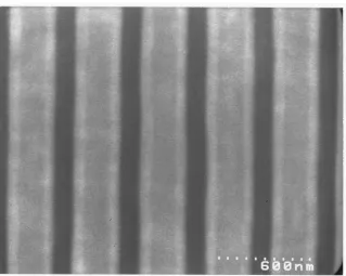
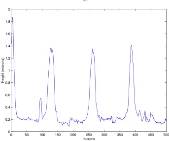
4.12 Surface map of channels in silicon dioxide obtained by atomic force microscopy. . . 54
4.13 Fused silica fluid channels used in fluorescent confocal microscopy measurements. . . . 54
4.14 Fluorescent measurement on beads in the 100 nm wide, 100 nm deep channels shown
4.15 Fused silica fluid channels used in fluorescent confocal microscopy measurements. The
channels are one micron wide spaced five microns apart. The row of “+” marks across
the middle of the image are used in aligning the channels with the confocal microscope. 55
[image:12.612.109.540.65.734.2]4.16 Fluorescent measurements on 63 nm beads in the 1µm wide, 100 nm deep channels of
Figure 4.15. . . 56
4.17 Confocal microscope configuration. . . 56
5.1 Velocity profile of pressure-driven flow in a capillary channel. . . 61
5.2 Electric double layer adjacent to a surface. . . 64
5.3 Electro-osmotic flow schematic illustrating water molecules, specifically adsorbed ions and hydrated solute molecules. . . 65
5.4 Channel etched in a silicon wafer and sealed with PDMS (silicone rubber). . . 67
5.5 Channel etched in an SOI wafer and sealed with PDMS. . . 68
5.6 Scanning Electron Micrograph of the Channels. . . 69
5.7 Photograph of the measurement setup showing PDMS reservoirs and platinum wire electrodes. . . 71
5.8 Measurement circuit; FC = fluid channel, CE = control electrode, Vg = control voltage to the back side of the silicon chip, Vs = excitation signal from the function generator. 71 5.9 Conductivity of channels with 100 mM NaCl solution (x) and deionized water (o). . . 72
5.10 100 mMN aSO4solution (x) compared against a control experiment in which no chan-nels were present on the silicon chip (o). . . 73
6.1 Electron-beam lithography used to define electrodes with a spacing of approximately 50 nm. . . 80
6.2 Geometry for electrode calculation. . . 80
6.3 Finite element model results showing the potential distribution between two spheres used to calculate their capacitance of 74.75289 aF. . . 82
6.4 Finite element model calculation of the potential distribution between two nanogap electrodes and the capacitance of the system. . . 83
6.5 Finite element model calculation of the potential distribution between two nanogap electrodes with a particle present between them offset 5 nm to the right of center. . . 84
6.7 Possible configuration in which a reference gap electrode is machined on the chip at
the same time as the sensing nanogap electrode. . . 86
6.8 Configuration using a pair of nanogap electrodes on the same fluid channel. . . 87
6.9 Example of a device containing a matched pair of nanogap electrodes with one electrode in common. The substrate material is Kaptonr. . . . 88
7.1 Charge/discharge circuit proposed by Lord Kelvin. . . 90
7.2 Oscillator capacitance measurement circuit. . . 91
7.3 Inductive-capacitive resonator circuit. . . 92
7.4 a. Wheatstone bridge for comparing resistances, G is a galvanometer. b. AC capaci-tance bridge for measuring capacicapaci-tances, D is a phase sensitive detector. . . 92
7.5 Single decade ratio transformer. . . 94
7.6 Three decade ratio transformer showing connection scheme for cascading multiple decade transformers. . . 95
7.7 Ratio transformer balanced capacitance bridge. . . 95
7.8 Device for testing the capacitance circuit. . . 96
7.9 Circuit connections for capacitance circuit testing using a precision ratio transformer to balance the AC bridge. . . 97
7.10 Measurement results of circuit in Figure 7.9. . . 97
7.11 Circuit connections for capacitance circuit testing using a half bridge configuration with no means of balancing the bridge. . . 98
7.12 Measurement results of circuit in Figure 7.11. . . 98
7.13 Device used to test nanogap electrode sensing of gold particles in solution. . . 99
7.14 Circuit connection for performing measurements on the nanogap electrodes. . . 99
Chapter 1
Introduction
1.1
Introduction
The objective of this research is to develop techniques for building electro-fluidic systems with
di-mensions less than 100 nm. These systems will be used to perform analytical measurements of
fluid and particle dynamics at nano-scale physical dimensions. The foundation for
accomplish-ing this task is to employ machinaccomplish-ing techniques typically used for buildaccomplish-ing integrated circuits and
micro-electromechanical systems. In this work, these traditional methods are further developed and
adapted for making sub-micron fluidic devices. In addition some important new techniques have
been developed for both defining features and etching them. The undercut etching technique
de-scribed in Chapter 2, Section 4 was developed in the course of this research to allow features less than
100 nm to be made using photoresist features larger than 1µm. One very useful etching technique
developed in this research is the xenon diflouride chemically assisted ion beam etching technique
presented in Chapter 3, Section 3. This method allows etching of features approaching 10 nm into
silicon using only organic resist films as an etch mask.
Chapter 4 reviews the fabrication and design of electrically interrogated nanofluidic systems.
Lithography and etching of the flow channels is described for a number of different material systems
which are promising candidates for the fabrication of nanochannels.
An additional goal of this work is to develop techniques by which fluids and particles can be
moved through sub-micron channels. In micron-scale fluidic systems, the most common method for
moving fluid volumes through micro-channels is with pressure driven flow. However many alternative
methods are worth exploring. In Chapter 5 various methods of driving fluids are compared for their
utility in nanometer size channels.
suspended particles in nanofluidic channels. Chapter 6 discusses design issues important for
max-imizing nanogap electrode sensitivity in response to changing properties of material contained in
nanofluidic channels. Chapter 7 discusses the measurement techniques necessary to detect small
changes in nanogap electrode capacitance in the presence of metallic particles.
1.2
Previous Work
Nanometer-scale fluid systems have been developed to perform analysis of DNA molecules by
study-ing and characterizstudy-ing their motion in various devices. Professor Craighead’s research group at
Cornell studied the dynamics of entropic trapping of DNA in channels less than 100 nm in height
[1, 2, 3]. Small pores machined in silicon nitride membranes are used to probe DNA molecules
elec-trically by monitoring the ionic current between solutions on either side of the membrane as DNA
molecules pass through the pore [4]. Professor Chu and his colleagues at Stanford have successfully
built 10 nm wide fluid channels [5, 6, 7].
Nanometer sized ionic pores in biological membranes control some of the most fundamental
processes of all organisms. They are in charge of regulating certain molecular reactions, transporting
ions through membranes, and are responsible for electrical signaling in neurons [8]. The micro- and
nano-structures of naturally occurring rocks and minerals result in a number of unique transport and
diffusion properties. These have in the past been utilized in many different applications, including
optics, electronics, filtration, data storage, and x-ray optics [9]. Materials such as carbon nanotubes
[10], macroporous silicon [11, 12], and aluminum oxide [13, 14] are currently being used in a number
of different experiments and engineering applications. The unique properties of zeolite materials
that allow them to function as molecular sieves are a result of a multitude of nanometer size pores
in the molecular structure [15, 16, 17, 18].
Methods of moving fluid through small-scale systems is an important area of research that is
necessary for the development of commercial devices. Inducing fluid flow by controlling the motion
of ions at liquid-solid interfaces is one of the more promising approaches.
Electrodes for sensing properties of the contents of fluid channels have been developed for
micron-scale system in order to measure properties of living cells. The device designed and built by Sohn et
al. demonstrated the ability to measure small capacitances of individual cells [19]. The externally
measured capacitance of a cell was shown to be primarily due to the quantity of DNA in the cell.
This was demonstrated by measurements performed on cells at different stages of mitosis.
sep-aration. One approach is to begin with a gap larger than desired and then reduce it by adding
material either through electro-deposition or shadow evaporation [20, 21]. An alternative approach
is to begin with a fine wire defined lithographically. Gradually etching, breaking, or locally heating
this wire eventually leads to the formation of a gap with molecular dimensions. In order to achieve
this, it is necessary to monitor the conductivity of the wire during this process [22, 23, 24, 25].
1.3
Nanometer-Scale Fluid Channels
Common physical properties of small channels and pores have a significantly different behavior than
their bulk counterparts. Physical and dynamic properties of small channels and pores deviate from
governing theory based on macro-scale fluid dynamics [26].
In particular, the non-slip boundary conditions of the Navier-Stokes equations are no longer
applicable when one is investigating the fluid dynamics very close to the boundary layer. Developing
a platform in which the details of small-scale fluid dynamics can be investigated in an artificially
controlled environment may be required to understand small-scale fluid dynamics and help discover
new uses for nanoporous materials.
1.4
Pumping Fluid in Nanometer Channels
Classical fluid mechanics describes large-scale fluid dynamics quite accurately. One of the common
assumptions is that non-slip conditions occur at the fluid boundary. This assumption is valid in
classical fluid dynamics because boundary conditions represent a small fraction of the fluid motion.
In the case of nanofluidics, this assumption is no longer valid, because the boundary flow comprises
a significant portion of the fluid motion. Thus it is of interest to describe how fluid flow can be
described in nanometer-sized channels.
In the case of this research, it is important to understand how particle motion can be influenced
by external physical stimuli. Effects that occur naturally, such as Brownian motion, work together
with methods for directing and controlling fluid flow. The overall motion is the superposition of all
these effects.
Brownian motion refers to the random movement of small particles suspended in a fluid. This
motion was first observed by early microscopists [27, 28]. Robert Brown, the Scottish botanist after
whom this type of motion is named, took a great interest in this topic. His careful experiments
himself. This motion was initially attributed to particles of biological origin, or “animacules.”
Experiments showed that this type of motion can also be observed in particles of non-organic origin
suspended in a fluid. Brown writes, “...extremely minute particles of solid matter, whether obtained
from organic or inorganic substances, when suspended in pure water, or in some other aqueous
fluids, exhibit motions for which I am unable to account, and which from their irregularity and
seeming independence resemble in a remarkable degree the less rapid motion of some of the simplest
animalcules of infusions [29].” The origin of Brownian motion was not satisfactorily explained until a
physical description based on molecular thermal motion was postulated by Albert Einstein [30, 31].
In the experiments presented here, the nanofluidic channel wall proximity reduces the magnitude
of observed Brownian movement [32, 33, 34]. In the extreme case, the particles are not able to pass
each other in the channels. This situation is referred to as single file diffusion [35]. In the case of
particles suspended in fluid channels, hydrodynamic coupling causes a correlation of particle position
and velocity [36, 37].
For this research it is necessary to exercise some degree of control over particle motion in the
channels. Ideally the particles can flow down the channel at a constant velocity. If this is not the case,
the interpretation of the data will become challenging. The methods that can be used to drive the
fluid flow at a constant rate include pressure differential [38, 39], temperature gradient [40], viscosity
gradient [40], electrolytic gradient (osmotic flow), electrical potential gradient (electro-diffusion) [41],
capillary action, acoustic waves [42, 43, 44, 45], rectified Brownian motion [46, 47, 48, 49], optical
tweezers [50, 51, 52], and radio frequency electromagnetic wave driven flow.
1.5
Nanometer-Scale Sensing Electrodes
Fluidic channels are constructed to physically confine fluids to a small region in space near electrodes.
The electrodes and the fluid between them make up an electrically coupled system used to perform
measurements on fluid or particles suspended in fluid.
The fluid channel size scale is below the resolution limit of optical microscopy, yet fluorescent
confocal microscopy is capable of detecting the motion of fluorescent particles or molecules in the
channels. Electronic techniques such as nuclear magnetic resonance [53], ionic current measurements
along the length of the channel [8], and capacitance measurements across the width of the channel
[54] have been used to measure properties of fluids and suspended particles in micrometer- and
nanometer-sized geometries. This research focuses on measuring changes in capacitance between
By placing electrodes on either side of a nano-channel, it is possible to measure capacitance
changes induced by metallic particles as they move past the electrodes. In order to maximize the
signal, electrodes must be comparable in size to the metallic particles. In addition, if a high degree
of spatial resolution is desired, it is necessary to make the electrodes as narrow as possible, without
References
[1] S. W. Turner, A. M. Perez, A. Lopez, and H. G. Craighead. Monolithic nanofluid sieving structures for DNA. Journal of Vacuum Science and Technology, 16(6):3835–3840, Novem-ber/December 1998.
[2] J. Han and H. G. Craighead. Entropic trapping and sieving of long dna molecules in a nanofluidic channel.Journal of Vacuum Science & Technology A-Vacuum Surfaces and Films, 17(4):2142– 2147, 1999.
[3] M. Foquet, J. Korlach, W. Zipfel, W. W. Webb, and H. G. Craighead. Dna fragment sizing by single molecule detection in submicrometer-sized closed fluidic channels. Analytical Chemistry, 74(6):1415–1422, 2002.
[4] Jiali Li, Derek Stein, Claran McMullan, Daniel Branton, Michael J. Aziz, and Jene A. Golovchenko. Ion-beam sculpting at nanometer length scales. Nature, 412:166–169, July 2001.
[5] W. L. Li, J. O. Tegenfeldt, L. Chen, R. H. Austin, S. Y. Chou, P. A. Kohl, J. Krotine, and J. C. Sturm. Sacrificial polymers for nanofluidic channels in biological applications. Nanotechnology, 14(6):578–583, 2003.
[6] H. Cao, J. O. Tegenfeldt, R. H. Austin, and S. Y. Chou. Gradient nanostructures for interfacing microfluidics and nanofluidics. Applied Physics Letters, 81(16):3058–3060, 2002.
[7] H. Cao, Z. N. Yu, J. Wang, J. O. Tegenfeldt, R. H. Austin, E. Chen, W. Wu, and S. Y. Chou. Fabrication of 10 nm enclosed nanofluidic channels. Applied Physics Letters, 81(1):174–176, 2002.
[8] Bertil Hille. Ionic Channels of Excitable Membranes. Sinauer, second edition, 1992.
[9] Mrs. E. J. Weichel-Moore and Dr. R. J. Potter. Fibre optical properties of ulexite. Nature, 200:1163–1165, 1963.
[10] J. Hone, M. C. Llaguno, M. J. Biercuk, A. T. Johnson, B. Batlogg, Z. Benes, and J. E. Fischer. Thermal properties of carbon nanotubes and nanotube-based materials. Applied Physics A-Materials Science & Processing, 74(3):339–343, 2002.
[11] J. Schilling, A. Birner, F. Muller, R. B. Wehrspohn, R. Hillebrand, U. Gosele, K. Busch, S. John, S. W. Leonard, and H. M. van Driel. Optical characterisation of 2-D macroporous silicon photonic crystals with bandgaps around 3.5 and 1.3µm.Optical Materials, 17(1-2):7–10, 2001.
[12] J. Schilling, F. Muller, S. Matthias, R. B. Wehrspohn, U. Gosele, and K. Busch. Three-dimensional photonic crystals based on macroporous silicon with modulated pore diameter.
Applied Physics Letters, 78(9):1180–1182, 2001.
[13] T. Doll, M. Hochberg, D. Barsic, and A. Scherer. Micro-machined electron transparent alumina vacuum windows. Sensors and Actuators A-Physical, 87(1-2):52–59, 2000.
[14] T. Doll, J. Vuckovic, M. Hochberg, and A. Scherer. Low-energy electron beam focusing in self-organized porous alumina vacuum windows. Applied Physics Letters, 76(24):3635–3637, 2000.
[15] J. M. D. MacElroy and S.-H. Suh. Equilibrium and nonequilibrium molecular dynamics studies of diffusion in model one-dimensional micropores. Microporous and Mesoporous Materials, 48:195–202, 2001.
[17] Volker Kukla, Jan Kornatowski, Dirk Demuth, Irina Girnus, Harry Pfeifer, Lovat V. C. Rees, Stefan Schunk, Klaus K. Unger, and J¨org K¨arger. NMR studies of single-file diffusions in unidimensional channel zeolites. Science, 272:702–704, May 1996.
[18] Vishwas Gupta, Sririam S. Nivarthi, Alon V. McCormick, and H. Ted Davis. Evidence for single file diffusion of ethane in the molecular sieve AlPO4-5.Chemical Physics Letters, 247:596–6000,
December 1995.
[19] L. L. Sohn, O. A. Saleh, G. R. Facer, A. J. Beavis, R. S. Allan, and D. A. Notterman. Capaci-tance cytometry: Measuring biological cells one-by-one.Biophysical Journal, 80(1):144A–144A, 2001.
[20] Y. V. Kervennic, H. S. J. Van der Zant, A. F. Morpurgo, L. Gurevich, and L. P. Kouwenhoven. Nanometer-spaced electrodes with calibrated separation.Applied Phyics Letters, 80(2):321–323, January 2002.
[21] A. F. Morpurgo, C. M. Marcus, and D. B. Robinson. Controlled fabrication of metallic electrodes with atomic separation. Applied Physics Letters, 74(14):2084–2086, April 1999.
[22] Hongkun Park, Andrew K. Lim, A. Paul Alivisatos, Jiwoong Park, and Paul L. McEwen. Fab-rication of metallic electrodes with nanometer separation by electromigration. Applied Physics Letters, 75(2):301–303, July 1999.
[23] X. E. He, S. Boussaad, B. Q. Xu, C. Z. Li, and N. J. Tao. Electrochemical fabrication of atomically thin metallic wires and electrodes separated with molecular-scale gaps. Journal of the Electroanalytical Chemistry, 522:167–172, 2002.
[24] J. L. Costa-Kr¨amer, N. Garc´ıa, P. Garc´ıa-Mochales, and P. A. Serena. Nanowire formation in macroscopic metallic contacts: quantum mechanical conductance tapping a table top. Surface Science, 342:L1144–L1149, 1995.
[25] Henk van Houten and Carlo Beenakker. Quantum point contacts. Physics Today, pages 22–27, July 1996.
[26] Liudmila A. Pozhar. Structure and dynamics of nanofluids: Theory and simulations to calculate viscosity. Physical Review E, 61(2):1432–1446, 2000.
[27] B. J. Ford. Brown observations confirmed. Nature, 359(6393):265–265, 1992.
[28] Brian J. Ford. Brownian movement in clarkia pollen: A reprise of the first observations. The Microscope, 40(4):235–241, 1992.
[29] Robert Brown. Additional remarks on active molecules. Philosophical Magazine, 6(161), 1829.
[30] Albert Einstein. ¨uber die von der molekularkinetischen Theorie der W¨arme gefordete Bewegung von in ruhenden Fl¨ussigkeiten suspendierten Teilchen. Annalen der Physik, 17:549, 1905.
[31] Albert Einstein. Investigations on the Theory of the Brownian Movement. Dover, 1956.
[32] Hilding Fax´en. Der Widerstand gegen die Bewegung einer starren Kugel in einer z¨ahen Fl¨ussigkeit, die zwischen zwei parallelen ebenen W¨anden eingeschlossen ist. Archiv F¨or Math-ematic, Astronomi och Fysik, 18(29):1–52, 1924.
[33] Alec T. Clark, Moti Lal, and Gill M. Watson. Dynamics of colloidal particles in the vicinity of an interacting surface. Faraday Discussions of the Chemical Society, 83:179–191, 1987.
[34] Luc P. Faucheux and Albert J. Libchaber. Confined brownian motion. Physical Review E, 49(6):5158–5163, June 1994.
[36] Binhua Lin, Bianxiao Cui, Ji-Hwan Lee, and Jonathan Yu. Hydrodynamic coupling in diffusion of quasi-one-dimensional Brownian particles. Europhysics Letters, 57(5):724–730, March 2002.
[37] Q.-H. Wei, C. Bechinger, and P. Leiderer. Single-file diffusion of colloids in one-dimensional channels. Science, 287:625–627, January 2000.
[38] C. L. Hansen, E. Skordalakes, J. M. Berger, and S. R. Quake. A robust and scalable microfluidic metering method that allows protein crystal growth by free interface diffusion. Proceedings of the National Academy of Sciences of the United States of America, 99(26):16531–16536, 2002.
[39] Mark A. Unger, Hou-Pu Chou, Todd Thorsen, Axel Scherer, and Stephen R. Quake. Monolithic microfabricated valves and pump by multilayer soft lithography. Science, 288:113–116, April 2000.
[40] Phillip Espinasse. Light directs fluid flow. OE Magazine, 3(10):7,9, October 2003.
[41] Richard B. M. Schasfoort, Stefan Schlautmann, Jan Hendrikse, and Albert van den Berg. Field-effect flow control for microfabricated fluidic networks. Science, 286:942–945, 1999.
[42] C. Lee and A. Lal. Low-voltage high-speed ultrasonic chromatography for microfluidic assays. InProceedings of the Solid State Sensor and Actuator Workshop, pages 206–209, Hilton Head Island, South Carolina, 2002.
[43] M. K. Araz, C. H. Lee, and A. Lal. Ultrasonic separations in microfluidic capillaries. In
Proceedings of the IEEE-UFFC Conference, Hawaii, 2003. IEEE.
[44] R. B. Hastings and Yung-Yao Shih. Experiments with an electrically operated kundt tube.
American Journal of Physics, 30:512–516, 1962.
[45] Robert A. Carman. Kundt tube dust striations. American Journal of Physics, 23:505–507, 1955.
[46] Deniz Ertas. Lateral separation of macromolecules and polyelectrolytes in microlithographic arrays. Physical Review Letters, 80(7):1548–1551, February 1998.
[47] Joel S. Bader, Richard W. Hammond, Steven A. Henck, Michael W. Deem, Gregory A. McDer-mott, James M. Bustillo, John W. Simpson, Gregory T. Mulhern, and Jonathan M. Rothberg. DNA transport by a micromachined Brownian ratchet device. Proceedings of the National Academy of the Sciences of the United States of America, 96(23):13165–13169, November 1999.
[48] Gary W. Slater, Hong L. Guo, and Grant I. Nixon. Bidirectional transport of polyelectrolytes using self-modulating entropic ratchets. Physical Review Letters, 78(6):1170–1173, February 1997.
[49] Alexander van Oudenaarden and Steven G. Boxer. Brownian ratchets: Molecular separations in lipid bilayers supported on patterned arrays. Science, 285:1046–1048, August 1999.
[50] Thomas T. Perkins, Stephen R. Quake, Douglas Smith, and Steven Chu. Relaxation of a single DNA molecule observed by optical microscopy. Science, 264:822–826, May 1994.
[51] Steven Chu. Laser manipulation of atoms and particles. Science, 253:861–866, August 1991.
[52] A. Ashkin. Optical trapping and manipulation of neutral particles using lasers. Proceedings of the National Academy of Sciences of the United States of America, 94:4853–4860, May 1997.
[53] Mladen Barbic. Magnetic resonance diffraction using the magnetic field from a ferromagnetic sphere. Journal of Applied Physics, 91(12):9987, 2002.
Chapter 2
Lithography Techniques for
Nanometer Sized Fluid Channels
and Electrodes
2.1
Introduction
Integrated circuit technology became practical as a result of advances in lithographic techniques
and development of thin film processing techniques [1]. These advances in lithography allowed
circuit designers to define increasingly smaller sized physical structures of circuit components and
connecting wires. Reducing component size not only allowed smaller circuits, but also enabled
operating at higher frequencies while consuming less power. This is the foundation of Moore’s
scaling law [2]. Advances in processing techniques permit building new types of active and passive
devices on a single semiconductor substrate. These techniques for building integrated circuits have
been borrowed for manufacturing micro-electromechanical systems (MEMS), nano-electromechanical
systems (NEMS), and microfluidic systems.
2.2
Sub-micron Scale Lithography
One of the most important technological advances in integrated circuits was the development of
a method of defining microscopic circuit elements accurately and repeatably. Initially, integrated
circuit components were fabricated by using a screen printing method originally designed for printing
photo reproductions [1]. This process involves using a thick paint to block the pores on a fine mesh
screen. Printing is performed by forcing a resist ink through the pores that are not blocked by the
Work Piece
Support Frame
Screen
Patterned Work Piece Work Piece
a.
b.
c.
d.
Pore−Blocking Paint
Resist Ink
Resist Ink
Figure 2.1: Screen printing process: a. The screen is attached to a rigid frame and patterned with pore-blocking paint. b. The screen is held against the work piece. c. Ink is forced through the pores and onto the surface of the work piece. d. The finished result is a pattern in the ink.
The smallest feature size that can be fabricated with this technique is limited by the size of the pores
in the screen. Typical pore sizes used for this technique are around 100 µm. This technology is
not capable of producing the micron-scale features required by modern microelectronics. However,
recent developments in nanoporous materials [3] suggests that the screen printing technique could
become useful in the mass production of nanopatterned media such as the magnetic storage surface
of computer disk drives [4, 5]. This approach was superseded by development of photosensitive resist
material capable of making smaller electronic devices integrated on a single chip [6, 7, 8, 9].
Advances in methods by which patterns are printed on semiconductor wafer surfaces was, and
still is, a major driving factor governing the development of integrated circuits. Current technology
is capable of producing features significantly smaller than the wavelength of light used for exposure
by exploiting a number of basic optical and chemical properties of the photolithography process.
2.3
Photolithography
The first challenge in defining microscopic devices is to precisely control the shape of each part. In
traditional machining, this is done by removing material with a cutting tool. In micro-machining,
material is removed by chemical or physical dissolution or erosion methods that remove material from
exposed surface areas. To machine specific shapes by etching requires patterned masks to protect
areas that should not be removed. Such masks are made of photo-sensitive polymers, called
Chrome Absorber
a.
b.
c.
d.
Substrate
Photoresist
UV Light
Exposed Photoresist
Unexposed Photoresist
Photoresist Remaining After Development Mask Plate
Mask Plate
Figure 2.2: Photolithography process steps: a. Align mask with the photoresist coated substrate. b. Bring the mask and substrate together, and expose the photoresist to ultra violet light through the mask. c. Develop the photoresist to remove exposed areas. d. After developing the substrate is ready for subsequent processing steps.
Figure 2.3: Cross-sectional view of photoresist stripes on a silicon wafer.
to light in selective regions and development in a chemical solution to define a pattern.
Photolithography is similar to developing a photographic emulsion. Light which falls on a piece
of photographic film induces local changes in the chemistry of the emulsion. In photography the
developing process causes the emulsion to change in areas exposed to light. Photoresists used
in photolithography differ from photographic emulsions in that a resist developer will remove the
exposed material rather than merely change its color. Once a pattern of resist has been defined
on the surface, the entire surface can be etched to selectively remove material not protected by the
resist, and transfer the resist pattern into the workpiece with high fidelity. The basic photoresist
2.4
Shadow Mask Lithography
In some applications, it is necessary to create device features that are smaller than the minimum
size obtainable with lithography processes that are commonly used. A number of techniques enable
the fabrication of sub-resolution features. The geometries possible with this technique are limited,
but, when used appropriately, surprising results are possible at little expense or effort. Moreover,
no specialized equipment is needed, and it may even be feasible to introduce these techniques into
commercial and manufacturable processes.
Angle Evaporation O
Photoresist
Directional Etch
d. c. a.
b.
[image:25.612.172.480.232.455.2]Substrate
Figure 2.4: Shadow mask process: a. Begin with a photoresist feature. b. Evaporate the metal etch mask at an angle Θ from normal. c. Pattern is transferred into the substrate with a directional etch. d. Final result after removal of the etch mask and photoresist.
The term “shadow mask” refers to the physical shadowing of a flux of atoms as they are deposited
onto the surface of the work piece. By placing the substrate at a given angle to the beam of material
as it is deposited, the profile of the photoresist creates a small gap adjacent to the photoresist, where
the substrate remains exposed [10]. Figure 2.4 shows a typical process which utilizes shadow masking
to etch a narrow channel. Figure 2.4 a. and b. illustrate the shadowing effect of the photoresist
during deposition of the evaporated material, Figure 2.4 c. illustrates the directional etch step, and
2.4 d. the final result. One important characteristic of shadow masking is that it will create a small
shadow on one side of a feature made in photoresist. Figure 2.5 shows a cross section of a sample
fabricated using the shadow masking technique. The substrate has been etched, but the photoresist
Figure 2.5: Cross-section of a fluid channel made with a shadow mask technique.
of the step depicted in Figure 2.4 c.
Processing steps for shadow mask lithography
1. Prepare and clean substrate1.
2. Vapor coat with HMDS adhesion promoter.
3. Spin coat photoresist (Shipley SPR3010)
4. Soft bake the photoresist on a hot plate with a surface temperature of 95 ◦C for 60 seconds.
5. Expose the photoresist through a mask.
6. Post exposure bake on a hot plate set to 105 ◦C for 60 seconds. This step is specifically for
SPR3010, some photoresists do not require a post exposure bake.
7. Develop the photoresist. For SPR3010 the developer used was MF-701 although a number of
similar developers work equally well. The developing time was 30 seconds.
8. Rinse with deionized water for 30 seconds.
Figure 2.6: Line made using shadow mask technique.
9. Spin dry the wafer by placing it back on the spin coater and spinning it at 5,000 RPM for 20
seconds.
10. Hard-bake the photoresist at 120◦C for 60 seconds.
11. Load the wafer into a metal evaporator with the surface tilted at the desired angle. Orient the
wafer to shadow the appropriate side of photoresist features.
12. Evaporate metal to deposit a layer only as thick as is absolutely necessary for future processing
steps.
In Figure 2.6 the roughness of the photoresist edge is fairly typical for photolithography, and
results from small pieces of photoresist that are either not removed in the developer, or that are
redeposited onto the surface as the developer is rinsed away. These small pieces of remaining material
can be removed by placing the sample in an oxygen plasma for a short time. This was not done in
the case of the sample shown, because the oxygen plasma cleaning would also round off photoresist
edges, and would result in a shadow with a less clearly defined edge.
Shadow masking has been found useful for making large numbers of devices with small features.
method was found to be useful only for simple devices, and is not appropriate for building nanometer
sized channels and electrodes along with larger connecting structures necessary for testing. The
increase in the number of required processing steps, low repeatability, and limitations on design
geometries make electron-beam lithography more practical for device prototyping.
Another technique closely related to shadow masking is an undercut etching technique. In this
approach, a layer of material just beneath the photoresist is etched away to leave a small gap
between the edge of the photoresist and the edge of the underlying layer (Figure 2.7 a, b). The
overhanging edge of photoresist is then used to shadow the small area beneath the metal during a
subsequent evaporation step (Figure 2.7 c). The evaporation is done with a beam of atoms incident
perpendicular to the surface. Removal of photoresist then leaves small channels on either side of
where the photoresist once was (Figure 2.7 d).
d. c. a.
b. Undercut Etch
Metal Evaporation
Photoresist Removal Photoresist
Substrate
Figure 2.7: Undercut etch technique: a. Begin with a photoresist feature on top of a mask material. b. Etch exposed mask areas with an isotropic etch to remove the mask material just under the photoresist edges. c. Deposit a second etch mask layer. The overhanging edge of the photoresist will create a small gap. d. Pattern is transferred into the substrate with a directional etch.
The layer beneath the photoresist can be any material applied to the surface with a uniform
thickness, and can be selectively etched with an etch that does not attack the photoresist or the
substrate. Chrome works very well for this application despite its tendency to form small crystalline
chrome etch used to undercut the photoresist consists of a mixture of ceric ammonium and acetic
acid manufactured by Transene Co. Inc [11]. The etch rate of this solution is very repeatable, and
slow enough that the amount of undercut can be precisely controlled.
Processing steps for undercut etching and evaporation
1. Prepare and clean substrate2.
2. Evaporate a thin layer of material to be undercut. The rate at which this material will be
undercut depends upon its thickness. A thinner layer will take longer to undercut, therefore
the amount of undercut can be controlled more precisely. In the case Figure 2.8 this layer
consisted of 50 nm of chromium.
3. Spin coat photoresist (Shipley SPR3010)
4. Soft bake the photoresist on a hot plate with a surface temperature of 95 ◦C for 60 seconds.
5. Expose the photoresist through a mask.
6. Post exposure bake on a hot plate set to 105 ◦C for 60 seconds. This step is specifically for
SPR3010, some photoresists do not require a post exposure bake.
2Substrate cleaning and preparation are discussed in Chapter 3.
7. Develop the photoresist. For SPR3010 the developer used was MF-701 although a number of
similar developers work equally well. The developing time was 30 seconds.
8. Rinse with deionized water for 30 seconds.
9. Spin dry the wafer by placing it back on the spin coater and spinning it at 5,000 RPM for 20
seconds.
10. Hard-bake the photoresist at 120◦C for 60 seconds.
11. Etch the underlying chromium layer using chrome etch for 10 seconds.
12. Load the wafer into a metal evaporator with the surface normal to the source flux.
13. Evaporate metal to deposit a layer only as thick as is absolutely necessary for future processing
steps.
14. Remove the photoresist using acetone.
In addition to metals, a few polymer materials have been specially designed to create an
under-cut profile. One that works quite well is the LOR series of chemicals manufactured by Microchem
Corporation [12]. This polymer is compatible with most photoresist processes and developers.
Be-cause the LOR is etched by many common photoresist developers, a separate etch step to create the
undercut profile is not necessary. The undercut profile is created by developing the photoresist for
a time slightly longer than what is required for a normal process.
This method is not very dependent on the cross-sectional profile of the features made in the
photoresist, which is often difficult to control. Additionally, the gap that is produced is uniform on
all edges of a feature instead of only one side as in shadow masking.
2.5
Electron-Beam Lithography
Electron-beam lithography is a technique that uses a focused electron beam to change the properties
of a resist layer [13]. Rather than using a mask as in optical lithography, the desired pattern is traced
out by the electron-beam. The instrument employed to do this is an electron microscope with a few
simple modifications which allow it to be used for electron-beam lithography. The X and Y scan
coils of the electron microscope are disconnected from the scan circuitry for normal operation, and
made with a computer drawing program, and converted to a series of X and Y beam movements
that trace the pattern on the sample surface with the electron-beam (Figure 2.9) [14, 15, 16].
Electron Source
Field Emission
Condenser Lens
Condenser Lens and
Sample
Pattern
Computer
Generator
Digital
to Analog
Converter
Scan Coils
Figure 2.9: Electron-beam lithography system.
Beam Electron
PMMA
Substrate PMMA
Substrate
a. b.
Figure 2.10: a. Electron-beam resist exposure. b. Electron-beam resist development.
The resist material in electron-beam lithography is exposed using electrons rather than photons
as in photolithography (Figure 2.10 a.). The most commonly used resist material is PMMA, or
polymethyl methacrylate. Some common names for this material are Plexiglas and acrylic. The
developer used is an organic solvent such as methyl isobutyl ketone and isopropyl alcohol (Figure
2.10 b.) [17]. Figures 2.11 and 2.12 show examples of patterns made using electron-beam lithography.
Electron-beam lithography processing steps.
These were the processing steps used to create the Caltech logo in Figure 2.11.
Figure 2.11: Caltech logo machined in a thin gold film on a silicon wafer.
2. Spin-coat PMMA at 10,000 RPM, resulting in a thickness of 90 nm for a solution of 2% 950K
molecular weight PMMA in chlorobenzine.
3. Bake the PMMA an a hot plate set to 180◦C for 30 minutes.
4. Place the sample on the SEM sample holder and load into the SEM.
5. Carefully align the SEM electron column, focus the beam and adjust the stigmators to obtain
the sharpest possible image.
6. Expose the pattern using a dose of 5 to 10 µC/cm2 with the beam voltage set to 30 kV.
7. Develop the pattern with a solution of one part MIBK (methyl isobutyl ketone) and three
parts IPA (isopropyl alcohol) for 30 seconds with gentle agitation.
8. Rinse with IPA for 30 seconds.
9. Blow the sample dry using compressed nitrogen.
10. Etch the chrome and gold using the patterned PMMA as the etch mask.
The resolution of electron-beam lithography is limited by the spot size of the electron-beam,
Figure 2.12: Etched lines in silicon patterned by electron-beam lithography and etching.
the electron spot size is in part due to scattering of electrons from resist molecules, and partially to
generation of secondary electrons that spread out in every direction. These effects have been studied
both experimentally and computationally using Monte Carlo analysis. Results indicate that beam
spreading is inversely proportional to the electron source accelerating voltage. Higher accelerating
voltage generally results in higher secondary electron yields, and implies that an optimal acceleration
voltage exists for a given type of sample, taking into consideration the type of electron sensitive
resist used, its thickness, and the secondary electron yield from the substrate [18]. In practice the
accelerating voltage is determined by the equipment being used. Most electron microscopes are
not capable of accelerating voltages larger than 30 kV. Production type electron-beam lithography
systems use accelerating voltages in the range of 50 kV to 100 kV. These high voltages are beneficial
for commercial systems because they allow greater process latitude, and can produce high aspect
ratio features in thick resist layers [19]. The disadvantage to high acceleration voltage is the increase
in pattern error as a result of proximity effect correction; certain areas will be overexposed as a
result of electron scattering while exposing adjacent features. Lower acceleration voltages require
2.6
Electron Image Projection System
Electron image projection system (ELIPS) is a technique that may solve the problem of low
through-put of electron-beam lithography [20]. Instead of using a sharply focused electron-beam to draw
exposure patterns in the resist, the ELIPS system uses a patterned electron emitter to
simultane-ously expose all of the desired features at the same time. Electrons emitted from the patterned
electron emitter are accelerated toward the sample by means of a bias voltage applied between the
emitter and sample. A magnetic field parallel to the electric field is used to prevent electrons from
spreading and blurring the resulting image. Early attempts at developing this lithography system
were not successful, due to an insufficiently uniform magnetic field over the sample surface.
Since this approach was first attempted, advances in superconducting magnets made stronger
and more uniform magnetic fields possible. This lithography technique was attempted using a
superconducting magnet from a NMR system with a bore diameter of 2.5 inches. This technique
was successful in transferring patterns with features of 100nm. Performance at this level was difficult
to achieve repeatably. The failure of this system to produce consistent results was most likely due
to a combination of many factors. The electrons are emitted from the patterned electron emitter
with random initial velocities. The electrons with an initial velocity not perpendicular to the sample
substrate result in a blurring of the features on the patterned electron emitter. The amount of
blurring is inversely related to the time required for the electron to travel from the emitter to the
sample.
2.7
Conclusion
Lithography is the single most important step in building nanometer scale devices. The techniques
presented here were developed in the process of this research. The most important aspect to keep
in mind when implementing these techniques is what process steps limit the overall resolution, and
why. For example in electron beam lithography, focusing the electron beam to the smallest possible
circular spot is more important than optimizing exposure doses or development times.
The most valuable processes are those in which the resolution limiting process is one that is fairly
easy to control. For example in undercut etching the undercut distance is determined by the etch
rate during undercutting. If this process is well characterized, it is possible to obtain an accuracy
of less than 50 nm.
un-dercut etching techniques that allow sub-micron patterning of some geometries obtained through
photo-lithography. These approaches are more easily adapted to automated mass production of
devices because they do not require the use of electron beam lithography. While this limits this
technique to pattens of simple design, it achieves resolution comparable with the best electron beam
References
[1] Jack S. Kilby. Invention of the integrated circuit. IEEE Transactions on Electron Devices, 23(7):648–654, 1976.
[2] Gordon E. Moore. Cramming more components onto integrated circuits. Electronics, 38(8), April 1965.
[3] Kornelius Nielsch, Jinsub Choi, Kathrin Schwirn, Ralf B. Wehrspohn, and Ulrich G¨osele. Self-ordering regimes of porous alumina: The 10% porosity rule. Nano Letters, 0(0):A–D, 2002.
[4] M. Barbic, S. Schultz, J. Wong, and A. Scherer. Recording processes in perpendicular pat-terned media using longitudinal magnetic recording heads. IEEE Transactions on Magnetics, 37(4):1657–1660, 2001.
[5] J. Wong, A. Scherer, M. Barbic, and S. Schultz. Perpendicular patterned media in an (Al0.9Ga0.1)2O3/GaAs substrate for magnetic storage. Journal of Vacuum Science & Tech-nology B, 17(6):3190–3196, 1999.
[6] Minoru Tsuda. Some aspects of the photosensitivity of poly(vinyl cinnamate). Journal of Polymer Science: Part A, 2:2907–2916, 1964.
[7] Minoru Tsuda. An interpretation of the optical sensitivity of poly(vinyl cinnamate). Polymer Letters, 2:1143–1146, 1964.
[8] L. M. Minsk, J. G. Smith, W. P. Van Deusen, and J. F. Wright. Photosensitive polymers. I. cinnamate esters of poly(vinyl alcohol) and cellulose. Journal of Applied Polymer Science, 2(6):302–307, 1959.
[9] E. M. Robertson, W. P. Van Deusen, and L. M. Minsk. Photosensitive polymers. ii. sensitization of poly(vinyl cinnamate). Journal of Applied Polymer Science, 2(6):308–311, 1959.
[10] Ivor Brodie and Julius J. Muray.The Physics of Micro/Nano-Fabrication. Microdevices Physics and Fabrication Technologies. Plenum Press, 1992.
[11] Chrome etchant CE-8002-A. Technical report, Transene Co. Inc., 10 Electronics Ave. Danveros MA 01923.
[12] LORTMlift-off resists. Technical report, Microchem Corp., 1254 Chestnut Street, Newton, MA
02464, 2002.
[13] SPIE Handbook of Microlithography, Micromachining and Microfabrication. SPIE.
[14] Haroon Ahmed. Single electron electronics: Challenge for nanofabrication. Journal of the Vacuum Society of America B, 15(6):2101–2108, November/December 1997.
[15] Shazia Yasin, D. G. Hasako, and H. Ahmed. Fabrication of <5nm width lines in poly(methylmethacrylate) resist using a water:isopropyl alcohol developer and ultrasonically-assisted development. Applied Physics Letters, 78(18):2760–2762, April 2001.
[16] Wei Chen and Haroon Ahmed. Fabrication of 5-7 nm wide etched lines in silicon using 100 kev electron-beam lithography and polymethylmethacrylate resist. Applied Physics Letters, 62(13):1499–1501, March 1993.
[17] Ilesanmi Adesida, Thomas E. Everhart, and R. Shimizu. High resolution electron-beam lithog-raphy on thin films. Journal of Vacuum Science and Technology, 16(6):1743–1748, Novem-ber/December 1979.
[19] Mark A. McCord. Electron beam lithography for 0.13µm manufacturing. Journal of Vacuum Science and Technology B, 15(6):2125–2129, November/December 1997.
Chapter 3
Fabrication Procedure for
Nanometer-Sized Fluid Channels
and Electrodes
3.1
Introduction
This chapter reviews processing techniques that are most relevant to nanofabrication. Processing
operations can be separated into individual steps that either add or remove material from the
surface. Combining these basic functions with lithography techniques described in the previous
chapter provide the basic set of tools necessary to build micro and nanometer-scale fluidic devices.
3.2
Thin Film Deposition
Thin film deposition is used to make the metal wires and insulating layers on integrated circuits.
Many types of optical coatings including reflective metal films, dielectric anti-reflective coatings,
and multilayer thin film mirrors are made using thin film deposition techniques. A wide variety of
techniques exist for depositing thin films onto surfaces. Only the techniques that are most relevant
to building nanometer-size devices will be considered here.
3.2.1
Thermal Evaporation
Thermal evaporation is by far the most widely used method of depositing thin films. A material is
simply heated in a vacuum chamber until it begins to vaporize. The vapor then condenses on the
surfaces inside the chamber. Any object exposed to the condensing vapor will be coated with a thin
it in a wire basket or a metal “boat” that is resistively heated by passing a large electrical current
through it, as illustrated in Figure 3.1 a [1, 2].
Source Material Vapor
Flux
Source Material
Vapor Flux
A Current Source
Electron Beam Work Piece
Work Piece
a.
b.
Figure 3.1: a. Thermal evaporation, b. Electron-beam evaporation.
3.2.2
Electron-Beam Evaporation
Electron-beam evaporation is a technique that uses an intense electron beam to heat the source
materials and cause thermal evaporation(Figure 3.1 b.). It can be applied to more materials than
thermal evaporation. Materials with high melting temperatures such as platinum and materials of
low thermal conductivity such as silicon dioxide can be processed by electron beam evaporation. The
method is also capable of evaporating materials at a rate much higher than thermal evaporation,
thus it is useful for situations where a thick layer needs to be deposited. The intense vapor flux
produced by electron beam evaporation allows rapid deposition [1, 2].
In a technique such as shadow mask lithography (Section 2.4) electron beam evaporation provides
a great advantage. The intense material flux rate allows placing the sample far from the source while
maintaining a reasonable evaporation rate. Placing the sample as far away from the source as possible
also produces a clearly defined edge to the shadow, similar to a shadow produced by the intense flux
of a collimated light beam. Evaporation from a shorter sample-source separation produces a fuzzy
edge, similar to a shadow resulting from a diffuse light source [1].
The electron beam evaporator used in this work was designed to have a maximum spacing
between the sample and the source of 25 cm. The shadow masks previously shown in Figures 2.6
3.2.3
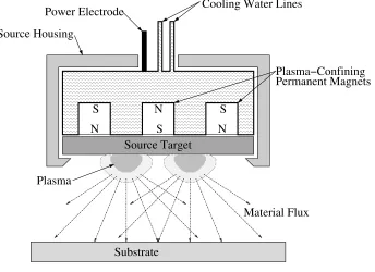
Sputtering
Sputtering is a method that uses a plasma to remove material from one surface to be deposited on
a second surface. Atoms or molecules are removed from one surface by bombarding it with ions
from a plasma magnetically confined to this surface. The flux of material from the source surface
condenses onto nearby surfaces creating a uniform coating (Figure 3.2) [3].
Plasma
N
S
S
N
Cooling Water Lines
[image:40.612.154.498.185.435.2]Substrate
Plasma−Confining
Permanent Magnets
Source Housing
Power Electrode
Source Target
Material Flux
N
S
Figure 3.2: Sputtering.
Sputtering differs from evaporation in that the atomic velocities are more randomly oriented as
they approach the sample surface. This explains why shadow effects seen in evaporation are normally
not seen with sputtering. This difference arises from three factors; the size of the sputtering source,
the source spacing, and the vacuum level during deposition. The source size and
sample-source spacing determine the amount of collimation of the flux. In electron beam lithography, flux
collimation was achieved by using a small source placed far from the sample in a ultra high vauccum
system. Sputtering uses a large source more closely spaced to the sample to achieve an opposite
effect. The pressure in the vacuum chamber is greater for sputtering than for evaporation. Greater
chamber pressure decreases the mean free particle path and increases their trajectory variation [2, 1].
Sputtering can deposit thin layers from a wide range of source materials because the source
need not be heated to its melting point. The most common methods of sputtering are magnetron
large voltage, or a high power radio frequency (13.5 MHz) signal. The plasma is confined to the
surface of the source material by a local magnetic field. In ion beam sputtering, an ion beam is
accelerated at the source target. In both of these techniques the source material is removed from
the source target through the collisions of energetic ions with the surface [3].
3.3
Etching
Etching is the basic method of removing material from a surface. Usually, it is necessary to remove
material only in certain areas. The areas that are not to be etched are protected by an etch mask.
In many cases, however, the etch mask material will be removed at the same time. One measure of
the quality of an etch process is the selectivity ratio; the relative etch rate of the mask layer to the
layer being etched.
3.3.1
Reactive Ion Etching
A plasma is started in a rare atmosphere of a reactive gas in a vacuum chamber (Figure 3.3 a). The
ionization process also dissociates the reactive gas into smaller, highly reactive, ionized molecules.
The variation in ion density creates a potential drop from the main body of the plasma to the lower
plate on which the material to be etched is placed (Figure 3.3 b). The effect of this potential drop
is to accelerate ions toward the surface. The high velocity ions impart kinetic energy to the surface
that increases the reaction rate, resulting in a faster etch rate on horizontal surfaces than vertical
features, making it possible to obtain sharp features with vertical walls (Figure 3.4) [2, 4, 5, 6, 7].
Figure 3.4 was made in a Materials Research Corporation reactive ion etching system under the
following conditions:
• C2F6flow rate: 25 sccm (standard cubic centimeters per minute)
• argon flow rate: 5 sccm
• chamber pressure: 35 mTorr
• electrode spacing: 3 inches (7.6 cm)
• power level: 60 Watts
• lower electrode voltage: 250 V
3.3.2
Ion-Beam Etching
Ion beam etching or milling is a very useful technique for creating nanometer-sized structures. It is
appropriate for etching features less than 20 nm in width. Ion beam etching erodes organic resist
materials very slowly, and results in vertical etch walls with little or no undercutting. The etch
mechanism does not depend on chemical reactivity, making this technique suitable for patterning
materials that would otherwise be problematic to etch.
Ion sources were originally developed as a method of spacecraft propulsion, and are commonly
used for positioning satellites [8]. Using electrostatics to accelerate a beam of ions away from the
spacecraft in turn results in a small motive force. Even though the acceleration provided by such a
drive is very small when compared to rocket propulsion, it is possible to accelerate the spacecraft to
high speeds over long distances in the vacuum of space. Because this type of propulsion does not
require bulky chemical propellants, ion propulsion is optimum for long missions where it would not
be practical to exclusively use chemical propellants.
Early in the development of ion propulsion systems it was noticed that the wall of the vacuum
test chamber at which the ion beam was directed began to develop pits on the surface. Application
of the ion beam technique to etching was quite obvious [9].
Ion beam production consists of a filament heated to a temperature resulting in thermionic
emission of electrons. The electrons are accelerated toward the anode. A magnetic field influences
their path so that instead of directly moving to the anode, they move in a circular orbit inside an
Ground Electrode
RF Oscillator RF Powered Electrode
Ground Electrode
Sample
b.
a.
Potential (Volts) 0
0 3.0
2.0
1.0
Distance From RF Powered Electrode (cm)
Impedance Matching Network
Figure 3.4: Channels etched in a fused silica microscope slide with a C2F6 reactive ion etching
process.
anode cup. When a gas molecule or atom collides with an electron, it is ionized and loses one or
more of its outer shell electrons. The ions then drift under the influence of the beam voltage toward
the accelerator grids. The voltage differential across the accelerator grids accelerates these ions and
collimates them into a beam directed towards the sample. In order to prevent excessive build up
of positive charge on the sample surface, an electron flux is added to the ion beam to result in
a net neutral charge. Electrons are added by a neutralizer filament through thermionic emission
[10, 11, 12, 13]. Figure 3.5 shows the basic components of an ion beam source.
If a neutralizing filament is not used, charge will build up on the surface of the sample, and
in a cloud of charged particles just above the surface. The presence of these charges will tend to
decelerate and deflect incoming ions, thus reducing the etch rate. The exact charge distribution
that results is very dependent on the sample material and its physical geometry. A consequence of
the cloud is non-reproducible etch rates. Even a conductive sample that is connected to ground will
tend to collect a charge cloud just above its surface. A second problem that can occur should the
voltage differential be large enough is an electrical discharge between the cloud of charge and the
sample surface. This creates very localized damage to areas of the substrate. The discharges are