Integrated Terahertz Graphene Modulator with 100% Modulation
Depth
Guozhen Liang,
†Xiaonan Hu,
†Xuechao Yu,
†Youde Shen,
‡Lianhe H. Li,
§Alexander Giles Davies,
§Edmund H. Lin
fi
eld,
§Hou Kun Liang,
∥Ying Zhang,
∥Siu Fung Yu,
⊥and Qi Jie Wang
*
,†,‡†OPTIMUS, School of Electrical and Electronic Engineering, and ‡CDPT, School of Physical and Mathematical Sciences, The
Photonics Institute, Nanyang Technological University, 50 Nanyang Avenue, Singapore 639798, Singapore
§School of Electronic and Electrical Engineering, University of Leeds, Leeds LS2 9JT, U.K.
∥Singapore Institute of Manufacturing Technology, 71 Nanyang Drive, Singapore 638075, Singapore ⊥Department of Applied Physics, Hong Kong Polytechnic University, Kowloon, Hong Kong
*
S Supporting InformationABSTRACT: Terahertz (THz) frequency technology has many potential applications in nondestructive imaging, spectroscopic sensing, and high-bit-rate free-space communi-cations, with an optical modulator being a key component. However, it has proved challenging to achieve high-speed modulation with a high modulation depth across a broad bandwidth of THz frequencies. Here, we demonstrate that a monolithically integrated graphene modulator can efficiently modulate the light intensity of the THz radiation from a THz quantum cascade laser with a 100% modulation depth for
certain region of the pumping current, as a result of the strongly enhanced interaction between the laserfield and the graphene enabled by this integration scheme. Moreover, the small area of the resulting device in comparison to existing THz modulators enables a faster modulation speed, greater than 100 MHz, which can be further improved through optimized designs of the laser cavity and modulator architectures. Furthermore, as the graphene absorption spectrum is broadband in nature, our integration scheme can be readily scaled to other wavelength regions, such as the mid-infrared, and applied to a broad range of other optoelectronic devices.
KEYWORDS: terahertz modulator, graphene, integrated photonics, quantum cascade laser, 100 percent modulation depth
L
ying between the microwave and mid-infrared, the terahertz (THz) frequency region of the electromagnetic spectrum (∼0.3 to 10 THz) has potential for a number of diverse applications ranging from nondestructive imaging1−5 and spectroscopic sensing6−8 through to ultrahigh-bit-rate wireless communication.9−11 Research in this region of the spectrum has undergone significant development over the last two decades, and the introduction and application of new materials such as graphene12−14 and metamaterials,15−17 together with the development of devices such as the quantum cascade laser (QCL)18−20and the THz quantum well infrared photodetector (THz QWIP),21−23 are bringing THz tech-nologies closer to more widespread application.An optical modulator is a key component widely used for beam manipulation, imaging, optical communication, and active mode locking in other parts of the electromagnetic spectrum. However, the development of fast and efficient THz modulators is in its infancy, compared with the significant advances made in THz frequency lasers and detectors. Attempts to fabricate THz amplitude modulators have so far focused on semiconductor heterostructures containing a two-dimensional electron gas (2DEG) in which electrons can be
accumulated or depleted by an applied gate voltage.24However, the modulation depth of such devices is ultimately limited by the achievable tunability in electron density, which is up to∼1 × 1012 cm−2 for a 2DEG in a conventional semiconductor
heterostructure.14These devices were, therefore, initially found to modulate the THz amplitude by only a few percent, although through the incorporation of metamaterials or plasmonic structures that enhance the interaction between the THz radiation and the 2DEG,15,25a modulation depth of 30% was achieved more recently. A more promising material for efficient THz modulation is graphene.26−28Its carrier concentration can be electrically tuned to be as high as 1 ×1014 cm−2, and its natural bidimensionality andflexibility allow easy incorporation with other materials and structures. Recently a modulation depth of∼15% was achieved in the 570−630 GHz frequency band through electrical gating of a graphene sheet,12and this was increased to ∼64% through use of plasmonic or cavity structures, albeit with a narrow bandwidth.14,29,30 However, further increase of the modulation depth has proved difficult,
Received: June 5, 2015
Published: October 19, 2015
Article
pubs.acs.org/journal/apchd5 This is an open access article published under a Creative Commons Attribution (CC-BY)
unless by stacking multiple graphene layers.31In addition, all the graphene modulators to date were studied as isolated components, with typically large active areas (tens of mm2)
required to facilitate optical alignment. The consequent large time constant of the effective RC circuit of the device limited the modulation speed of such graphene modulators to only ∼13 MHz.14 Although this is similar to that found in semiconductor modulators,25 a much higher modulation speed ought to be possible in graphene-based modulators owing to the material’s ultrahigh intrinsic carrier mobility (>20 000 cm2 V−1 s−1 for graphene on SiO
2 at room
temperature).32
To explore the full potential of graphene, the monolithic integration of a graphene modulator with a THz radiation source is a promising solution. The benefits are threefold:first, miniaturization will increase the modulation speed owing to reduced parasitic capacitance and resistance of the device; second, a larger modulation depth may be achieved as a stronger interaction of the THz radiation with the graphene layer is possible; and, finally, the integration eliminates one stage of optical alignment and the associated bulky mirrors or lenses.
Here, we report, for thefirst time, the realization of graphene modulators integrated with surface-emitting concentric-circular-grating (CCG) THz quantum cascade lasers33,34for achieving a 100% modulation depth with a fast modulation speed. By employing the CCG as a feedback element,33,34steady single-mode THz QCL operation can be obtained with relatively high
output power. We demonstrate that a 100% modulation depth can be achieved as a consequence of a strong interaction of the graphene with the laserfield, which is greatly enhanced at the output apertures of the laser cavity. Moreover, the small device area of the device allows fast modulation that could be further improved through optimized design of the laser cavity and the modulator architecture. Furthermore, since graphene has a broadband absorption spectrum,35our integration scheme can readily be scaled to other wavelength regions. For example, it can be easily extended to the mid-infrared (mid-IR) regime by monolithically integrating mid-IR QCLs with graphene. In addition, the proposed scheme will enable the realization of mid-IR and THz integrated optical circuits, combined with other photonic components such as detectors, waveguides, and
filters, for communication, sensing, and spectroscopy applica-tions.
[image:2.625.154.471.68.379.2]■
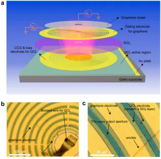
DEVICE OVERVIEWFigure 1a shows a schematic illustration of the integrated device, which consists of an underlying surface-emitting CCG THz QCL with a graphene modulator, the Fermi level of which can be dynamically tuned by a voltage (Vgr) applied to the gating electrode. The active region of the QCL, with a peak gain at around 3 THz, is sandwiched between a bottom gold plate and the upper CCG metal grating. The CCG was designed as a second-order grating such that single-mode THz radiation will be emitted vertically through the grating Figure 1.Overview of the quantum cascade laser integrated graphene modulator. (a) Schematic illustration of the device. Only the central few rings of the circular-concentric grating (CCG) (orange region) are connected together with the spoke bridges to allow electrical pumping of the quantum cascade laser (QCL) over a small active region. Light is emitted vertically from the surface and is modulated by the electrically gated graphene. (b) Optical microscope images showing the central part of a fabricated device. The bonded gold wire for electrical driving of the QCL is also shown in the image. (c) Enlarged view showing details of the graphene and the QCL electrodes, which are insulated by a 450 nm thick SiO2layer. A wrinkle resulting from folding of transferred chemical vapor deposition (CVD) graphene is visible at the lower right corner.
apertures, which is then modulated by the electrically gated graphene. To facilitate graphene transfer, the active region of the QCL was not etched to keep the upper surface as flat as possible. Thus, the laser cavity is formed solely by the CCG itself. Additionally, only the central few rings of the CCG (the orange region inFigure 1a) are connected together with spoke-like metal bridges to allow electrical pumping over a small active region beneath. This restricted the otherwise high current in the QCL to only a few amperes. With the correct CCG design, the optical modes are confined in the pumped area so that the QCL maintains a sufficiently low threshold current for lasing action (seeSupporting Information). On top of the CCG, a SiO2layer insulates the QCL electrode from the
graphene gate electrode; this is followed by the graphene sheet. The device fabrication is assisted by patterning the graphene gate electrode before the introduction of the graphene sheet.
Figure 1b shows optical microscope images of the central part of a fabricated device. The enlarged view inFigure 1c shows the
details of the graphene and QCL electrodes, which are insulated by the SiO2 layer. A wrinkle resulting from folding
of the transferred chemical-vapor-deposition-grown (CVD) graphene is visible at the lower right corner.
■
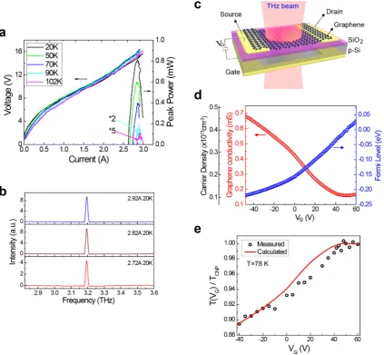
SEPARATE CHARACTERIZATIONS OF THE THZ CCG QCL AND THE GRAPHENEWefirst characterized the THz CCG QCL with the graphene electrodefloating. The QCL lased under pulsed operation (500 ns pulse width, 10 kHz repetition rate) up to a 102 K heat sink temperature (Figure 2a), compared with∼135 K for a typical ridge laser (200μm wide and 1.5 mm long) fabricated from the same QCL wafer. Surface-emitting single-mode lasing was obtained at all temperatures and pump currents. Figure 2b shows the laser spectra as a function of current at a heat sink temperature of 20 K.
[image:3.625.102.526.68.459.2]To characterize the properties of the CVD-grown graphene, a separate graphene modulator was fabricated on a SiO2/Si
Figure 2.Separate characterization of the THz QCL and the graphene layer. (a) Light−current−voltage (LIV) characteristics of the THz CCG QCL at different heat sink temperatures. (b) Laser spectra as a function of pump currentI, at 20 K. It shows a single-mode operation over the whole dynamic range of THz CCG QCLs. (c) Schematic representation of the structure used to characterize the graphene layer. It is noted that the bottom gate metal layer under the graphene area was opened for THz beam transmission. (d) Direct current conductivity, carrier density, and Fermi energy of the graphene as a function of gate voltage, measured at 78 K. (e) Gate voltage dependence of the modulation of the THz transmitted intensity (∼3 THz) by the graphene, showing a modulation depth of∼11% over the applied bias range from−40 to 60 V. The effect of the silicon substrate on the experimentally measured modulation has been removed using a transfer matrix method. Before removing this substrate effect, the modulation depth is 17%.
substrate, as shown schematically inFigure 2c, using the same CVD graphene sheet (seeMethods). The 450 nm thick SiO2
layer was formed by plasma-enhanced CVD (PECVD) and was identical to that used for the QCLs. Raman spectroscopy was used to confirm that the graphene sheet after transfer was both high quality and a monolayer (Figure S2, Supporting Information). In view of the fact that the QCL-integrated devices will be operated under cryogenic conditions, we investigated the electrical and optical absorption properties of the graphene at 78 K (the QCL surface and active region are typically several tens of Kelvin higher than the heat sink temperature). Using a simple model to fit the gate-voltage-dependent sheet resistance of the graphene (see Supporting Information), we obtained the gate-voltage-dependent sheet conductivity, carrier density, and Fermi energy of the graphene, as plotted inFigure 2d. The inherent p-type doping of the CVD graphene is confirmed by the reduction in conductivity with increasing gate bias, up to the Dirac point (Vg ≈50 V). The graphene conductivity and carrier density were found to change from 0.16 mS to 0.65 mS and from 0.1×1013cm−2to 0.45× 1013cm−2, respectively, as the gate bias was increased from−40
V to +60 V. Correspondingly, the Fermi energy was tuned from
−230 meV to +20 meV. The nonzero conductivity at the Dirac point is due to a residual carrier concentration of 0.1 ×1013 cm−2, resulting from charged impurities.36
Although the use of a back-gate structure, which features a relatively small capacitance, limits the range of carrier density and Fermi energy tuning possible (a top gating scheme could realize a carrier density as high as 1013−1014 cm−2),37
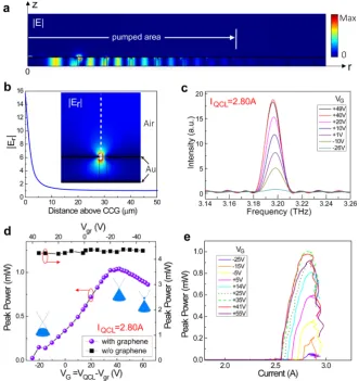
[image:4.625.146.478.68.420.2]the tunability of the carrier density in graphene is still much larger than that achieved in 2DEGs arising from semiconductor heterostructures. As the optical absorption of graphene in the THz region is dominated by intraband optical transitions (i.e., free carrier absorption), this larger tunability in carrier density, along with the generally high mobility of graphene (∼900 cm2 V−1s−1 at 78 K in our case), makes graphene a much more efficient THz wave modulator than alternative semiconductor devices. Normalized to the maximum light transmission at the Dirac point,TDir, a modulation depth of ∼11% in transmitted power (T(Vg)/TDir) was observed for our graphene modulator upon sweeping the gate voltage from −40 V to +60 V, measured at 78 K, using a standard ridge waveguide 3.0 THz QCL as the radiation source (fabricated from the same wafer as used for the CCG QCL of our integrated device) (Figure 2e). Figure 3.Integrated graphene modulation of a CCG QCL. (a) Cross-sectional view of the calculated electricfield distribution of the CCG QCL. A white arrow indicates the electrically pumped area. (b) Amplitude of the electricfield (Er) near the output aperture of the CCG QCL along the white dashed line in the inset, which is the cross-sectional view of the|Er|distribution near a CCG aperture. (c) Enhanced modulation of the THz wave by the integrated graphene modulator. The intensity of the lasing peak varies from nearly zero atVG=−26 V to a maximum atVG= +40 V. (d)VG dependence of the output power of the CCG QCL with (circles) and without (rectangles) the graphene. The pumping current of the QCL is 2.80 A. (e) Light−current characteristics of the QCL as a function ofVGconfirming that a 100% modulation depth is achieved when the pumping current of the THz QCL is less than 2.78 A. For higher pumping current of the QCL (2.78−2.93 A), the THz radiation cannot be totally suppressed, but we can still obtain a modulation depth of 94% in the worst case (when the injection current to the QCL is∼2.85 A).
Here, the effect of the Si substrate on the modulation was removed using a transfer matrix method,12and the measured result agrees well with theoretical analysis (Figure 2e, see
Supporting Informationfor details). It is worth noting that the optical absorption of graphene in the THz region of the spectrum differs fundamentally from that at visible and near-infrared frequencies, where interband optical transitions dominate, resulting in only a∼2.3% intensity modulation.
■
INTEGRATED GRAPHENE MODULATION OF CCG QCLSA larger modulation strength is expected when the graphene is integrated with a THz CCG QCL owing to the electricfield enhancement in the graphene near the output aperture of the QCL.Figure 3a plots the cross-sectional view of the calculated electric field distribution of the CCG QCL. As only the horizontally polarized component of the electric field (Er) is
responsible for the THz emission into the far field, we investigated theErdistribution around the CCG apertures, with
a representative cross-sectional plot shown in the inset of
Figure 3b. The curve inFigure 3b describes the|Er|field profile along the white dashed line of the inset, indicating a great enhancement of|Er|in the aperture region. For a SiO2spacing
thickness of 450 nm, it is estimated that|Er|is enhanced by a
factor of 12 in the graphene region, which corresponds to an intensity enhancement factor of∼140. The resulting enhanced modulating effect of graphene on the CCG QCL is shown in
Figure 3c, where the intensity of the lasing peak varies from nearly zero at VG = −26 V to a maximum at VG = +40 V. During measurement, the QCL was biased at 14.8 V (corresponding to an injected current of 2.80 A) in pulsed mode operation (500 ns pulse width, 10 kHz repetition rate) at a 20 K heat sink temperature, and the graphene was gated at a series of dc biasesVGdefined byVG= VQCL−Vgr, withVQCL
being the voltage applied to the QCL electrode and Vgr the voltage applied to the graphene electrode (seeFigure 1a). The solid circles inFigure 3d show the average laser output power as a function of VG, which is consistent with the results in Figure 2d and e. As a comparison, a control device without the graphene sheet was fabricated, and the output power is plotted as a function ofVGas rectangles inFigure 3d, with no obvious modulation being observed. Note that in the presence of the graphene the output power decreases significantly; the power of the integrated device atVG= +40 V is around a quarter of that
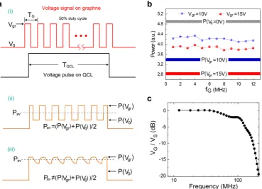
[image:5.625.130.500.68.335.2]from the control device. To verify the effect of the graphene modulator further, we measured the light−current curves of the laser at a series of graphene gate voltages, as shown inFigure 3e. As it indicates, for the pumping current of the THz QCL below 2.78 A, the integrated device allows a 100% modulation depth (|ΔT|/TMax) of the THz radiation amplitude, as the emission vanishes when the graphene is biased with a large enough negative voltage. For higher pumping current of the QCL (2.78−2.93 A), the THz radiation cannot be totally suppressed, but we can still obtain a modulation depth of 94% in the worst case (when the injection current to the QCL is Figure 4.Measurement of the modulation speed of the integrated graphene modulator. (a) (i) Device bias scheme. The pulse duration for the QCL wasfixed atTQCL= 1μs (corresponding to a frequency offQCL= 1 MHz), while an ac rectangular signal was applied onto the graphene electrode with 50% duty cycle and various periods ofTG=TQCL/N(fG=NfQCL), whereNis an integer. (ii) Predicted output optical signal of the device if the graphene modulator is able to follow the variation of the applied voltage. In this case, the average peak powerPav= (P(Vgr) +P(V0))/2, whereP(Vgr) andP(V0) are the output peak powers when a constantVgrorV0is applied to the graphene electrode, respectively. (iii) Predicted output optical signal of the device if the applied signal to the graphene is faster than the speed of the modulator, in which casePavdeviates from (P(Vgr) +P(V0))/2. (b)Pavas a function of modulation frequencyfG. The blue line (star symbols) corresponds toV0= 0 V andVgr= 10 V, while the red line (circle symbols) corresponds toV0= 0 V andVgr= 15 V. The gray-, blue-, and red-shaded ribbons indicate the output power when the graphene electrode is dc biased at 0, 10, and 15 V, respectively. The widths of the ribbons reflect the instability of laser power during the measurement period. (c) Frequency response of the graphene modulator.
∼2.85 A). It is worth mentioning that although the graphene was put above the cavity, it actually interacts with the evanescent waves of the cavity mode through the output apertures. Therefore, when gating the graphene at different voltages, its refractive index varies, leading to a slight change of the effective refractive index of the laser cavity and, thus, a slight shift of the lasing peak, as can be seen inFigure 3c.
■
MODULATION SPEED OF THE INTEGRATED GRAPHENE MODULATOROwing to the lack of suitable fast THz detectors, we cannot observe the time-varying THz modulated signal directly to determine the operational speed of the modulator. Therefore, the modulation speed is estimated by monitoring the average output power of the device while an ac voltage signal is applied to the graphene electrode, as shown inFigure 4a(i). The pulse duration for the QCL isfixed atTQCL= 1μs (corresponding to a frequency offQCL= 1 MHz), while the ac rectangular signal
on the graphene has a 50% duty cycle and a period of TG =
TQCL/N(fG=NfQCL), whereN is an integer. If the graphene
[image:6.625.67.256.622.713.2]modulator can follow the variation of the applied voltage, the output optical signal of the device will be as that shown in
Figure 4a(ii), and the average power (Pav) detected experimentally should be (P(Vgr) + P(V0))/2 regardless of
the modulation frequency, where P(Vgr) and P(V0) are the output peak powers when constant gating voltagesVgrandV0
are applied to the graphene electrode, respectively. Otherwise, as illustrated inFigure 4a(iii),Pav will deviate from (P(Vgr) + P(V0))/2. Therefore, one could expect aflatPavvsfGcurve up to a cutoffpoint, where the correspondingfGis approximately
the modulation speed of the device. The measured Pav vs fG
curve is shown in Figure 4b, in which the blue line (star symbols) corresponds toV0= 0 V andVgr= 10 V, while the red line (circles) corresponds to V0 = 0 V and Vgr = 15 V. The
gray-, blue-, and red-shaded ribbons indicate the output powers when the graphene electrode is dc biased at 0, 10, and 15 V, respectively. The widths of the ribbons indicate the instability of the laser power during the measurement period. A flat dependency was observed up to 12 MHz, the limit of our experimental facilities, with no cutoff point, which already makes it one of the fastest THz modulators. To extend the measurement range, we investigated the dynamic response (S21) using a radio frequency (RF) network analyzer. Using this together with an equivalent circuit model, we obtained the frequency response of the integrated modulator (Figure 4c; see
Supporting Informationfor details). The modulation speed can therefore be estimated to be 110 MHz from the 3 dB cutoff point.
The electrical modulation on the graphene sheet is given by (seeSupporting Information)
ω ω ω ω ω = + + + × + ≈ + + × + V
V i R C R R i C
i R C
i R C C i R C
1
1 /( 1/ )
1 1
1
1 ( )
1 1 pt
p
G
S 0 0 G t G t G t G t
0 t Gt Gt Gt (1) where VS and VG are the amplitude of the voltage on the graphene electrode and that applied to the graphene sheet, respectively,R0is the internal impedance of the RF source (50 Ω),RGt is the effective graphene resistance, CGt andCpt are the
total capacitance of the graphene sheet and the metal contacts, respectively, andωis the angular frequency of the modulation. In eq 1, we assumed RGt ≪ 1/iωC
G
t for our case. Two time
constants,τ1=R0(Cpt+CGt) andτ2=RGtCGt, then determine the
cutofffrequency. Thefirst time constant can be decreased by reducing the size of the graphene back gate (i.e., the QCL bias contact), which requires a smaller cavity design. The second time constant can be decreased by reducing the widths of the graphene electrode slits (this makes the effective area of the graphene sheet smaller so that the graphene capacitance is smaller) and by reducing the graphene resistance. The graphene resistance is dominated by the contact resistance at the metal/graphene edges and can be reduced though several techniques reported in the literature.38−40
■
DISCUSSIONFor QCLs, direct modulation of the laser itself can be very fast by microwave injection (>10 GHz for ridge-waveguide device41). However, in this direct modulation case, as the pumped current and voltage keep changing, the gain profile and the refractive index, as well as the temperature, of the active region are varying rapidly, making the laser frequencyfluctuate, i.e., the frequency chirping effect. Our scheme could allow the laser to operate more stably because now the modulation is performed by changing the graphene voltage, but not the laser. Although our devices do not totally get rid of the chirping effectafter all, the frequency shift in Figure 3c is perceivableit could be expected that they have a smaller chirping effect since the effective refractive index change induced by the gating graphene is much smaller than that induced by the modulating gain medium. Therefore, our scheme may be advantageous in applications where the chirping effect is not desired. In addition, our device may also be used as a whole as a THz modulator for free-space light modulation with the active region of the QCL unpumped or pumped below the threshold, so that it is suitable for many other occasions where their own light sources are used.
■
CONCLUSIONSWe have reported a THz graphene modulator, monolithically integrated with a surface-emitting CCG QCL, that shows a modulation depth in the range of 94−100% and a response speed of 110 MHz. The high modulation depth is a consequence of a strong interaction of the graphene with the laserfield, which was further enhanced at the output apertures of the laser cavity, while the high modulation speed is due to the reduced device area enabled by the integration. Even faster operation frequency could be achieved through further improvements to the device architecture. Our integration scheme can also be applied to the mid-infrared and near-infrared frequency ranges, as the optical absorption of graphene is naturally broadband.
■
METHODSPreparation of the Graphene Film. The commercially sourced CVD-grown graphene on copper foil was spin-coated with a poly(methyl methacrylate) (PMMA) film, which was then fully cured in a 110 °C oven for 5 min, resulting in a PMMA thickness of∼1μm. The copper substrate was etched by floating the PMMA/graphene/copper sheet on an ammonium persulfate (0.1 M, Sigma-Aldrich) solution for >3
h. After rinsing, the PMMA/graphene film was ready for transfer.
Fabrication of the Isolated Graphene Modulator. A 450 nm thick layer of SiO2was blanket deposited on a lightly
doped p-type Si substrate (resistivity 1−20 Ω·cm) using PECVD. The source, drain, and back electrodes were formed by electron-beam evaporation, after which the PMMA/ graphene film (1 cm× 1 cm) was transferred and contacted with source and drain electrodes. The sample was dried in air, followed by annealing in nitrogen at 160 °C for 3 h. The PMMA layer was then removed in acetone.
Fabrication of the Integrated Devices with Graphene Modulator and CCG QCL. The active region of the THz QCL was grown by molecular beam epitaxy on an undoped GaAs substrate. Fabrication of the devices commenced with gold−gold thermocompression bonding of the active region to an n+ GaAs receptor wafer. The original QCL substrate was then removed through lapping and selective chemical etching. This was followed by the removal of the highly absorbing contact layer of the active region to prevent attenuation of the THz radiation that couples out of the grating slits. Top metal gratings (Ti/Au/Ti 15/300/10 nm) were defined by standard optical lithography and lift-off; the top 10 nm Ti layer was used as an adhesive between the Au and the subsequent SiO2
insulation layer, which was grown by PECVD. After patterning the SiO2 layer to allow electrical access to the QCL, another
optical lithography and lift-offprocess was carried out to define the graphene electrode on top of the SiO2/CCG rings. A
graphene sheet was then transferred onto the graphene electrode, followed by annealing in nitrogen at 160 °C for 3 h to relax the PMMA/graphene film slowly and make full contact with the surface underneath. After removing the PMMA layer with acetone, the graphene was patterned to remove unwanted material area and avoid contacting the other electrodes. The samples were then cut and indium-mounted onto Cu submounts, wire-bonded, and finally attached to the coldfinger of a cryostat for measurement.
■
ASSOCIATED CONTENT*
S Supporting InformationThe Supporting Information is available free of charge on the
ACS Publications website at DOI: 10.1021/acsphoto-nics.5b00317.
Detailed structure parameters of the THz CCG QCL and its far-field characterization; Raman spectra of the transferrd graphenes; model used to retrieve the graphene parameters (carrier density, Fermi level, etc.) from electrical characterization; comparison of the graphene optical response at 78 and 300 K; high-frequency circuit model of the graphene modulator (PDF)
■
AUTHOR INFORMATION Corresponding Author *E-mail: [email protected]. Author ContributionsG.Z.L. and Q.J.W. conceived the idea. G.Z.L. designed the device. G.Z.L. and X.N.H. fabricated the devices. X.C.Y. and Y.D.S. helped in graphene preparation. G.Z.L. carried out the experimental measurements and the data analyses, built the theoretical models, and prepared the figures. L.H.L., A.G.D., and E.H.L. performed the growth of the QCL active region.
G.Z.L. and Q.J.W. wrote the manuscript. A.G.D. and E.H.L. revised the manuscript. H.K.L, Y.Z., and S.F.Y. improved the manuscript presentation. All authors reviewed the manuscript. Notes
The authors declare no competingfinancial interest.
■
ACKNOWLEDGMENTSWe acknowledgefinancial support from the EPSRC (UK), the EC Programme (TOSCA), and the Royal Society and Wolfson Foundation.
■
REFERENCES(1) Chan, W. L.; Deibel, J.; Mittleman, D. M. Imaging with Terahertz Radiation.Rep. Prog. Phys.2007,70, 1325−1379.
(2) Kim, S. M.; Hatami, F.; Harris, J. S.; Kurian, A. W.; Ford, J.; King, D.; Scalari, G.; Giovannini, M.; Hoyler, N.; Faist, J.; Harris, G. Biomedical Terahertz Imaging with a Quantum Cascade Laser.Appl. Phys. Lett.2006,88, 153903.
(3) Nguyen, K. L.; Johns, M. L.; Gladden, L.; Worrall, C. H.; Alexander, P.; Beere, H. E.; Pepper, M.; Ritchie, D. A.; Alton, J.; Barbieri, S.; Linfield, E. H. Three-Dimensional Imaging with a Terahertz Quantum Cascade Laser. Opt. Express 2006, 14, 2123−
2129.
(4) Lee, A. W. M.; Qin, Q.; Kumar, S.; Williams, B. S.; Hu, Q.; Reno, J. L. Real-Time Terahertz Imaging over a Standoff Distance (>25 Meters).Appl. Phys. Lett.2006,89, 141125.
(5) Tonouchi, M. Cutting-Edge Terahertz Technology. Nat. Photonics2007,1, 97−105.
(6) Mittleman, D. M.; Jacobsen, R. H.; Neelamani, R.; Baraniuk, R. G.; Nuss, M. C. Gas Sensing Using Terahertz Time-Domain Spectroscopy.Appl. Phys. B: Lasers Opt.1998,67, 379−390.
(7) Federici, J. F.; Schulkin, B.; Huang, F.; Gary, D.; Barat, R.; Oliveira, F.; Zimdars, D. THz Imaging and Sensing for Security Applicationsexplosives, Weapons and Drugs.Semicond. Sci. Technol. 2005,20, S266−S280.
(8) Ren, Y.; Hovenier, J. N.; Higgins, R.; Gao, J. R.; Klapwijk, T. M.; Shi, S. C.; Klein, B.; Kao, T.-Y.; Hu, Q.; Reno, J. L. High-Resolution Heterodyne Spectroscopy Using a Tunable Quantum Cascade Laser around 3.5 THz.Appl. Phys. Lett.2011,98, 231109.
(9) Koenig, S.; Lopez-Diaz, D.; Antes, J.; Boes, F.; Henneberger, R.; Leuther, A.; Tessmann, A.; Schmogrow, R.; Hillerkuss, D.; Palmer, R.; Zwick, T.; Koos, C.; Freude, W.; Ambacher, O.; Leuthold, J.; Kallfass, I. Wireless Sub-THz Communication System with High Data Rate.
Nat. Photonics2013,7, 977−981.
(10) Kleine-Ostmann, T.; Nagatsuma, T. A Review on Terahertz Communications Research. J. Infrared, Millimeter, Terahertz Waves 2011,32, 143−171.
(11) Chen, Z.; Tan, Z. Y.; Han, Y. J.; Zhang, R.; Guo, X. G.; Li, H.; Cao, J. C.; Liu, H. C. Wireless Communication Demonstration at 4.1 THz Using Quantum Cascade Laser and Quantum Well Photo-detector.Electron. Lett.2011,47, 1002.
(12) Sensale-Rodriguez, B.; Yan, R.; Kelly, M. M.; Fang, T.; Tahy, K.; Hwang, W. S.; Jena, D.; Liu, L.; Xing, H. G. Broadband Graphene Terahertz Modulators Enabled by Intraband Transitions. Nat. Commun.2012,3, 780.
(13) Vicarelli, L.; Vitiello, M. S.; Coquillat, D.; Lombardo, A.; Ferrari, a C.; Knap, W.; Polini, M.; Pellegrini, V.; Tredicucci, a. Graphene Field-Effect Transistors as Room-Temperature Terahertz Detectors.
Nat. Mater.2012,11, 865−871.
(14) Lee, S. H.; Choi, M.; Kim, T.-T.; Lee, S.; Liu, M.; Yin, X.; Choi, H. K.; Lee, S. S.; Choi, C.-G.; Choi, S.-Y.; Zhang, X.; Min, B. Switching Terahertz Waves with Gate-Controlled Active Graphene Metamate-rials.Nat. Mater.2012,11, 936−941.
(15) Chen, H.-T.; Padilla, W. J.; Zide, J. M. O.; Gossard, A. C.; Taylor, A. J.; Averitt, R. D. Active Terahertz Metamaterial Devices.
Nature2006,444, 597−600.
(16) Choi, M.; Lee, S.; Kim, Y.; Kang, S.; Shin, J. A Terahertz Metamaterial with Unnaturally High Refractive Index. Nature 2011,
470, 369−373.
(17) Watts, C. M.; Shrekenhamer, D.; Montoya, J.; Lipworth, G.; Hunt, J.; Sleasman, T.; Krishna, S.; Smith, D. R.; Padilla, W. J. Terahertz Compressive Imaging with Metamaterial Spatial Light Modulators.Nat. Photonics2014,8, 605−609.
(18) Köhler, R.; Tredicucci, A.; Beltram, F.; Beere, H. E.; Linfield, E. H.; Davies, A. G.; Ritchie, D. A.; Iotti, R. C.; Rossi, F. Terahertz Semiconductor-Heterostructure Laser.Nature2002,417, 156−159.
(19) Jung, S.; Jiang, A.; Jiang, Y.; Vijayraghavan, K.; Wang, X.; Troccoli, M.; Belkin, M. A. Broadly Tunable Monolithic Room-Temperature Terahertz Quantum Cascade Laser Sources. Nat. Commun.2014,5, 4267.
(20) Li, L.; Chen, L.; Zhu, J.; Freeman, J.; Dean, P.; Valavanis, A.; Davies, A. G.; Linfield, E. H. Terahertz Quantum Cascade Lasers with > 1 W Output Powers.Electron. Lett.2014,50, 309−311.
(21) Liu, H. C.; Song, C. Y.; SpringThorpe, A. J.; Cao, J. C. Terahertz Quantum-Well Photodetector.Appl. Phys. Lett.2004,84, 4068.
(22) Cai, X.; Sushkov, A. B.; Suess, R. J.; Jadidi, M. M.; Jenkins, G. S.; Nyakiti, L. O.; Myers-Ward, R. L.; Li, S.; Yan, J.; Gaskill, D. K.; Murphy, T. E.; Drew, H. D.; Fuhrer, M. S. Sensitive Room-Temperature Terahertz Detection via the Photothermoelectric Effect in Graphene.Nat. Nanotechnol.2014,9, 814−819.
(23) Chen, S.-L.; Chang, Y.-C.; Zhang, C.; Ok, J. G.; Ling, T.; Mihnev, M. T.; Norris, T. B.; Guo, L. J. Efficient Real-Time Detection of Terahertz Pulse Radiation Based on Photoacoustic Conversion by Carbon Nanotube Nanocomposite.Nat. Photonics2014,8, 537−542. (24) Kleine-Ostmann, T.; Dawson, P.; Pierz, K.; Hein, G.; Koch, M. Room-Temperature Operation of an Electrically Driven Terahertz Modulator.Appl. Phys. Lett.2004,84, 3555.
(25) Shrekenhamer, D.; Rout, S.; Strikwerda, A. C.; Bingham, C.; Averitt, R. D.; Sonkusale, S.; Padilla, W. J. High Speed Terahertz Modulation from Metamaterials with Embedded High Electron Mobility Transistors.Opt. Express2011,19, 9968−9975.
(26) Novoselov, K. S.; Geim, A. K.; Morozov, S. V.; Jiang, D.; Zhang, Y.; Dubonos, S. V.; Grigorieva, I. V.; Firsov, A. A. Electric Field Effect in Atomically Thin Carbon Films.Science2004,306, 666−669.
(27) Tassin, P.; Koschny, T.; Soukoulis, C. M. Graphene for Terahertz Applications.Science2013,341, 620−621.
(28) Novoselov, K. S.; Fal’ko, V. I.; Colombo, L.; Gellert, P. R.; Schwab, M. G.; Kim, K. A Roadmap for Graphene.Nature2012,490, 192−200.
(29) Sensale-Rodriguez, B.; Yan, R.; Rafique, S.; Zhu, M.; Li, W.; Liang, X.; Gundlach, D.; Protasenko, V.; Kelly, M. M.; Jena, D.; Liu, L.; Xing, H. G. Extraordinary Control of Terahertz Beam Reflectance in Graphene Electro-Absorption Modulators.Nano Lett.2012,12, 4518−
4522.
(30) Gao, W.; Shu, J.; Reichel, K.; Nickel, D. V.; He, X.; Shi, G.; Vajtai, R.; Ajayan, P. M.; Kono, J.; Mittleman, D. M.; Xu, Q. High-Contrast Terahertz Wave Modulation by Gated Graphene Enhanced by Extraordinary Transmission through Ring Apertures. Nano Lett. 2014,14, 1242−1248.
(31) Wu, Y.; La-o-vorakiat, C.; Qiu, X.; Liu, J.; Deorani, P.; Banerjee, K.; Son, J.; Chen, Y.; Chia, E. E. M.; Yang, H. Graphene Terahertz Modulators by Ionic Liquid Gating.Adv. Mater.2015,27, 1874−1879.
(32) Liao, L.; Bai, J.; Qu, Y.; Lin, Y.; Li, Y.; Huang, Y.; Duan, X. High-Kappa Oxide Nanoribbons as Gate Dielectrics for High Mobility Top-Gated Graphene Transistors.Proc. Natl. Acad. Sci. U. S. A.2010,107, 6711−6715.
(33) Liang, G.; Liang, H.; Zhang, Y.; Khanna, S. P.; Li, L.; Giles Davies, A.; Linfield, E.; Fatt Lim, D.; Seng Tan, C.; Fung, Y. S.; Chun Liu, H.; Wang, Q. J. Single-Mode Surface-Emitting Concentric-Circular-Grating Terahertz Quantum Cascade Lasers.Appl. Phys. Lett. 2013,102, 031119.
(34) Liang, G.; Liang, H.; Zhang, Y.; Li, L.; Davies, a. G.; Linfield, E.; Yu, S. F.; Liu, H. C.; Wang, Q. J. Low Divergence Single-Mode Surface-Emitting Concentric-Circular-Grating Terahertz Quantum Cascade Lasers.Opt. Express2013,21, 31872.
(35) Ren, L.; Zhang, Q.; Yao, J.; Sun, Z.; Kaneko, R.; Yan, Z.; Nanot, S.; Jin, Z.; Kawayama, I.; Tonouchi, M.; Tour, J. M.; Kono, J. Terahertz and Infrared Spectroscopy of Gated Large-Area Graphene.Nano Lett. 2012,12, 3711−3715.
(36) Adam, S.; Hwang, E. H.; Galitski, V. M.; Das Sarma, S. A Self-Consistent Theory for Graphene Transport.Proc. Natl. Acad. Sci. U. S. A.2007,104, 18392−18397.
(37) Efetov, D. K.; Kim, P. Controlling Electron-Phonon Interactions in Graphene at Ultrahigh Carrier Densities.Phys. Rev. Lett.2010,105, 256805.
(38) Hsu, A.; Wang, H.; Kim, K. K.; Kong, J.; Palacios, T. Impact of Graphene Interface Quality on Contact Resistance and RF Device Performance.IEEE Electron Device Lett.2011,32, 1008−1010.
(39) Leong, W.; Gong, H.; Thong, J. Low-Contact-Resistance Graphene Devices with Nickel-Etched-Graphene Contacts.ACS Nano 2014,8, 994−1001.
(40) Smith, J.; Franklin, A.; Farmer, D.; Dimitrakopoulos, C. Reducing Contact Resistance in Graphene Devices through Contact Area Patterning.ACS Nano2013,7, 3661−3667.
(41) Maineult, W.; Ding, L.; Gellie, P.; Filloux, P.; Sirtori, C.; Barbieri, S.; Akalin, T.; Lampin, J.-F.; Sagnes, I.; Beere, H. E.; Ritchie, D. A. Microwave Modulation of Terahertz Quantum Cascade Lasers: A Transmission-Line Approach.Appl. Phys. Lett.2010,96, 021108.