University of Tasmania
Design of a 32-bit Arithmetic Unit
based on Composite Arithmetic and
its Implementation on a Field
Programmable Gate Array.
by
Tomasz Hubert Pinkiewicz, BAppComp
A dissertation submitted to the
School of Computing
in partial fulfilment of the requirements for the degree of
Bachelor of Computing with Honours
Declaration
I hereby state that this thesis contains no material which has been
accepted for the award of any other degree or diploma in any
tertiary institution, and that, to the candidate’s knowledge and
belief, the thesis contains no material previously published or
written by another person except where due reference is made in
the text of the thesis.
Tomasz Pinkiewicz
Abstract
TABLE OF CONTENTS
CHAPTER 1: INTRODUCTION
1.1COMPUTER ARITHMETIC... 1
1.2 FIELD PROGRAMMABLE GATE ARRAYS... 5
1.3 OBJECTIVES AND OUTLINE OF RESEARCH... 7
CHAPTER 2: SIMPLE COMPOSITE ARITHMETIC MACHINE
DESIGN
2.1 COMPOSITE ARITHMETIC UNIT... 92.2 REGISTER UNIT... 20
2.3 CONTROL UNIT ... 23
2.4 INPUT/OUTPUT INTERFACE UNIT ... 27
CHAPTER 3: SIMPLE COMPOSITE ARITHMETIC MACHINE
SIMULATION
3.1 COMPOSITE ARITHMETIC UNIT... 303.2 REGISTER UNIT... 39
3.3 CONTROL UNIT ... 41
3.4 INPUT/OUTPUT INTERFACE UNIT ... 44
CHAPTER 4: CONCLUSIONS
4.1 RESULTS ... 464.2 RELEVANCE OF THE THESIS ... 46
4.3 FURTHER RESEARCH... 46
REFERENCES... 48
APPENDICES
APPENDIX A: SIMPLE COMPOSITE ARITHMETIC MACHINE... 49APPENDIX B: SIMULATIONS... 50
LIST OF FIGURES
FIGURE 1. PROPOSED EXACT STORAGE FORMS INCLUDE (A) PRIMARY EXACT FORM (INTEGER) AND (B) SECONDARY EXACT FORM (RATIONAL). IN THE BIT NUMBERING AS SHOWN, N STANDS FOR THE NUMBER OF BITS IN THE FORM AND CAN BE 32, 64, 128, OR 256, WHILE M NUMBERS THE DIFFERENT
FORM. ... 4
FIGURE 2. SIMPLE COMPOSITE ARITHMETIC MACHINE (SCAM). THE THICK RECTANGLE SHOWS CIRCUITS OF THE CAU... 9
FIGURE 3. GCD CIRCUIT FOLLOWS EUCLID'S ALGORITHM TO FIND GREATEST COMMON DIVISOR... 11
FIGURE 4. CAST CIRCUIT CASTS OUT COMMON FACTORS OF TWO 16-BIT NUMBERS. ... 13
FIGURE 5. SWAP CIRCUIT IS USED IN CONJUNCTION WITH DIVISION OPERATION. ... 14
FIGURE 6. MULTIPLY IS THE MOST IMPORTANT CIRCUIT BECAUSE IT IS USED WITH DIVISION, ADDITION AND SUBTRACTION OPERATIONS. ... 15
FIGURE 7. ADD CIRCUIT. ... 16
FIGURE 8. SUBTRACT CIRCUIT... 17
FIGURE 9. COPY CIRCUIT... 18
FIGURE 10. MOVE CIRCUIT... 19
FIGURE 11. REGISTER UNIT. ... 20
FIGURE 12. 32-BIT REGISTER CONSISTS OF TWO 16-BIT REGISTERS... 21
FIGURE 13. SCAM'S CONTROL WORD... 23
FIGURE 14. CONTROL UNIT. ... 24
FIGURE 15. FEEDBACK UNIT... 26
FIGURE 16. INPUT/OUTPUT INTERFACE UNIT... 27
FIGURE 17. LOAD CIRCUIT... 28
FIGURE 18. STORE CIRCUIT. ... 29
FIGURE 19. GCD SIMULATION. ... 30
FIGURE 20. CASTING SIMULATION... 31
FIGURE 21. SWAP SIMULATION... 32
FIGURE 22. MULTIPLY SIMULATION. ... 33
FIGURE 23. DIVIDE SIMULATION. ... 34
FIGURE 24. ADD SIMULATION. ... 35
FIGURE 25. SUBTRACT SIMULATION... 36
FIGURE 26. COPY SIMULATION... 37
FIGURE 27. MOVE SIMULATION... 38
FIGURE 28. 32-BIT REGISTER SIMULATION... 39
FIGURE 29. REGISTER ADDRESS DECODING SIMULATION. ... 40
FIGURE 30. OPERATIONS DECODING SIMULATION... 41
FIGURE 31. REGISTER SELECTION SIMULATION... 42
FIGURE 32. FEEDBACK SIMULATION... 43
FIGURE 33. LOAD SIMULATION. ... 44
FIGURE 34. STORE SIMULATION. ... 45
FIGURE 35. SCAM DIAGRAM SHOWING MAIN COMPONENTS... 49
FIGURE 36. CLOCK SIMULATION... 50
FIGURE 37. SIMULATION ONE... 51
FIGURE 38. SIMULATION TWO. ... 52
FIGURE 39. SIMULATION THREE. ... 53
FIGURE 40. SIMULATION FOUR... 55
FIGURE 41. SIMULATION FIVE. ... 57
FIGURE 42. AN8 LOGIBLOX MODULE. ... 58
FIGURE 43. AN16 LOGIBLOX MODULE. ... 59
FIGURE 44. AN32 LOGIBLOX MODULE. ... 60
FIGURE 45. BUF2 LOGIBLOX MODULE. ... 61
FIGURE 46. BUF4 LOGIBLOX MODULE. ... 62
FIGURE 47. BUFFER16 LOGIBLOX MODULE. ... 63
FIGURE 48. COMPARE16 LOGIBLOX MODULE... 63
FIGURE 49. EQUAL16 LOGIBLOX MODULE... 64
FIGURE 50. O16 LOGIBLOX MODULE. ... 65
FIGURE 51. SELECTOR16 LOGIBLOX MODULE. ... 66
Acknowledgments
I would like to thank Dr. Tariq Jamil, my supervisor, who introduced me to the FPGA concept, gave me great feedback on the work, and helped me with some critical problems that were slowing me down. He also encouraged me to share my work with others by writing paper for a conference. Also special thanks go to Neville Holmes for providing a subject for my thesis. His advice on determining the scope of the project and explanations of the concept were invaluable. Also recognition goes to the Academic Staff of the School of Computing for providing me with knowledge and problem solving skills required during the project design.
On the administrative side, thanks go to Xilinx Corporation for providing me with a FPGA device as part of the company’s University Program. Also appreciation goes to secretaries of the School, Raelene Couch and Yvette Kitchener and to the Technical Staff of the School, Tony Gray and Christian McGee.
1.1 Computer Arithmetic
1.1.1 Computer Arithmetic History
Fixed-point arithmetic was first used after World War Two to perform calculations on integer values and to represent them exactly. A programmer had several lengths of representation to cope with expected range of numbers. In integer arithmetic, calculation of fractions was done using scaling and this could produce inexact results (Neville 1997a and b). The scaling required for problems to be pre-processed by the user and then they could be accommodated by fixed point-representation. However with increasing speed of computers, more complex operations had to be performed and the pre-processing became a lengthy task (Kulisch, 1999). Also large numbers introduced a new concept into computer arithmetic, called overflow. To overcome the overflow problem, floating-point arithmetic was introduced.
Floating-point arithmetic can cope with large range of numbers, but it does so only by approximating. The numbers are represented in semi-logarithmic form and they have two components, significand and exponent. The significand expresses the precision of the number while the exponent expresses the range of the values that can be represented. This floating-point representation became a standard and is used in all older and modern computers. However, this notation has many problems, which have been accepted (or ignored) over the years.
calculations. (Kulisch 1999) describes five equations, all of them containing the same numbers with the same signs but arranged differently. Conventional computer with floating-point standard returns different values for each equation, while they all should be the same. Several other examples are provided which prove that even simple mathematical equations can be miscalculated when using floating-point form.
Another type of problem is concerned with programming issues. The programmer has to determine beforehand if fixed-point or floating-point notation should be used and what precision should be used (single or double). Then there is a problem of handling exceptions, and problem of converting between different forms and how this affects accuracy of result. Another concern is the accuracy of the display and how exceptions and special values will be displayed. All this has to be considered by the programmer and wrong decision can cause erroneous results.
Floating-point representation is an improvement over fixed-point form. However, today’s computers have become faster and have to perform more accurate and larger calculations. Current technology and requirements make the floating-point form “obsolete” and a new type of computer arithmetic is needed. One of the examples of advanced computer arithmetic is scalar product concept presented by (Kulisch 1999).
1.1.2 Advanced Computer Arithmetic
Advanced arithmetic expands the arithmetic and mathematical capability of the digital computer. It allows for twelve fundamental data types or mathematical spaces and highest degree of accuracy. The four basic ones are real, complex, interval and complex interval data types. It also allows for matrix and vector operations. Number of complex computations is increasing and more accuracy is needed. Advanced Computer Arithmetic offers improvement of floating-point arithmetic and gives more accurate results. Current research is aimed at incorporating these advanced concepts into the new microprocessors to avoid the bottleneck of Input/Output interface.
1.1.3 Composite Arithmetic
Composite Arithmetic (Neville, 1997a) is based on advanced computer arithmetic concept and combines several different formats. These are stored as a single binary form and formats are distinguished using tags. The storage form is specified by multiples of 16 and four lengths are recommended: short (32 bits), normal (64 bits), long (128 bits) and extended (256 bits). For most commercial calculations on exact numbers and scientific computations on inexact numbers, 32- and 64-bit sizes would be sufficient. The long and extended formats (128- and 256-bit) can be used for financial and number theory calculations, where very long exact results can occur. Also some intermittent technical computations where very precise results are needed would use one of these two formats. Composite arithmetic merges both exact and inexact formats using a tag bit. The bit is set to 0, if the number is exact and it is set to 1, if it is inexact.
between numerator and denominator. The solution to that is called a floating slash and it is several bits, depending on word length that separate the numerator from denominator. For example, for a 32-bit number, five bits are needed to be stored to accommodate the floating slash. If the numerator is 1 then all bits are available for the denominator. If the denominator is 1 then the number will be stored in an integer format; therefore the smallest denominator is 2. There are other issues, which have to be addressed when using this form. First, the denominator can be 0, which means that the number is infinity. Infinity needs storing because it can result from division by zero. Also indeterminate result needs storing.
Figure 1. Proposed exact storage forms include (a) primary exact form (integer) and (b) secondary exact form (rational). In the bit numbering as shown, n stands for the number of
bits in the form and can be 32, 64, 128, or 256, while m numbers the different form.
If the value cannot be stored exactly then the composite arithmetic will store it in an inexact form. Numbers can be represented in different ways. The first one is called double-number form. An example of it is the floating-point representation. The second one is called single-number form and an example of it is relatively new, signed logarithmic form. This form is subdivided into primary inexact and secondary inexact forms. Primary form uses signed pure logarithmic representation and secondary form uses antitetrational representation. The second form has been adopted by the Composite Arithmetic.
exact values uses decimal point and a fraction point. This would allow a number 456 ¾ to be represented as 456.3.4, where first dot is a decimal point and second dot is a fraction point. A number ½ would be stored as 0.1.2. This approach would also allow displaying infinity as 0.1.0 and indeterminacy 0.0.0. Representation of inexact numbers would be similar to the e-notation, where the exponent uses scaling base of 10. The display form would use the scaling base of 1000 and this would be called k-notation. This would be supported by m-notation (milli notation) to avoid squeezing a negative sign into the exponent. A second k or m could display secondary inexactness.
The proposal also mentions register form. This would be a fixed-point long accumulator, which would be 512 bytes (4096 bits) long. It would be large enough to store extended primary inexact storage form and some additional data like tags and signs.
Composite arithmetic is more complex than floating-point but many aspects of it have already been implemented in hardware and software. Replacing floating-point arithmetic would benefit electronic calculator arithmetic and would improve capabilities of software packages such as spreadsheets. Another advantage lies in programming using the composite arithmetic. The programmer wouldn’t have to make choices between fixed and floating point and all conversions would be done in the register form. Also the accuracy of results, especially for technical computation, would be much greater.
1.2 Field Programmable Gate Arrays
processor. The problem, which arises here for computer designers, is cost. If an ASIC is designed for a specified task and the task is slightly modified after the design is finished, then the ASIC will probably be incapable of solving the modified problem. If a modified ASIC can be developed to solve the new problem, the original hardware may be too highly customised to be reused in the new design. This will significantly increase the cost of the design and therefore cost of the final product.
New advances in electronics allow for a third solution. This is a use of large, fast, Field Programmable Gate Arrays (FPGAs). These circuits can be modified at almost any point during not only development but during the use. FPGAs consist of arrays of Configurable Logic Blocks (CLBs). They are like switches with multiple inputs and single output and they are used to perform operations such as AND, NAND, OR, NOR, XOR, etc. While in most hardware device logical functions of gates cannot be modified, in FPGAs, however, sending signals to the chip can change logic functions and the connections between the CLBs. This means that FPGAs can be re-programmed continuously and perform wide range of tasks with high speed and lower cost.
The structure of FPGA consists of a number of Configurable Logic Blocks and a programmable grid of connections that can link CLBs in any way depending on the design. The coarse-grained FPGAs have a small number of powerful CLBs; the fine-grained structure has many simple blocks. This means that a single element in a coarse-grained FPGA may be capable of adding or comparing two numbers, while one block in a fine-grained FPGA might be capable of comparing only two binary digits.
Other fields, where configurable computing can be successful, are pattern matching and encryption systems. Pattern matching is used in tasks such as handwriting recognition, face identification, database retrieval, and automatic target recognition. In case of target recognition, which is a military application, the greatest issue is the rapid comparison of an input image to thousands of templates. Another application mentioned above is encryption systems. There are ASICs, which are designed for only one kind of encryption algorithm. Configurable Computing would allow changing keys and algorithms and it would therefore make the encryption more secure and more convenient. The DES algorithm implemented on FPGAs is using 13,000-gate FPGA instead of 25,000-gate device previously required (Villasenor and Mangione-Smith 1997). These two examples show enormous flexibility of FPGAs. This, combined with increasing capacity and speed of FPGAs, can be used in digital communications, design automation and digital filtering for radar, while decreasing the cost of design.
Configurable Computing is still under development. Current FPGAs can have up to 100,000 logic elements and this will increase with further advances in technology. It is expected that by the end of the decade, FPGAs with a million logic elements will be developed. These will be used in highly complex communications and signal processing applications. Another possible application of FPGAs is Dynamic Instruction Set Computer (DISC). This would allow storing large number of circuit configurations, which could be activated by a programmer using a function call. Thanks to their flexibility, speed and overall cost, Field Programmable Gate Arrays provide lots of opportunity in many areas of computer science.
1.3 Objectives and Outline of Research
2.1 Composite Arithmetic Unit
[image:15.595.133.556.230.714.2]The Composite Arithmetic Unit is the main objective of the thesis. The arithmetic operations presented here will form a basis for future versions of the CAU and allow carrying out arithmetic operations on rational numbers. Sections 2.1.1 and 2.1.2 describe Greatest Common Divisor and Casting Circuits respectively. Section 2.1.3 contains Swap Circuit. Multiply and Divide operations are in Section 2.1.4 and 2.1.5. Sections 2.1.6 and 2.1.7 describe Add and Multiply Circuits. The last two sections 2.1.8 and 2.1.9 describe Copy and Move Circuits.
2.1.1 Greatest Common Divisor Circuit
The function of the circuit is to calculate the Greatest Common Divisor (GCD) of numerator and denominator of a rational number. The outcome of this operation is a number, which can be used with the rational number to cast out the common factors and reduce the size of the number.
The algorithm for finding GCD is based on the Euclid’ s Algorithm. There are several variations of the Euclid’ s Algorithm (including binary algorithm used in computing) but the following algorithm is a simple recursive function and can be easily implemented using hardware components.
int gcd(int m, int n) // m is numerator, n is denominator
{
if (m < n) // when numerator is greater than denominator
{
m = gcd (m, n - m); // make a recursive call with adjusted denominator
return m; }
else if (m > n) // when numerator is less than denominator
{
m = gcd (m - n, n); // make a recursive call with adjusted numerator
return m; }
else
return m; // When numerator equals denominator, // Stop and return the numerator (m), // Which holds the GCD of (m,n)
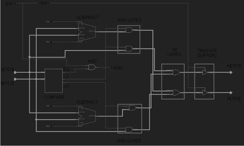
Figure 3. GCD Circuit follows Euclid's Algorithm to find Greatest Common Divisor.
Two input data buses are A [15:0] (denominator) and B [15:0] (numerator). The EN line enables the outputs and is used to generate the END signal. The output data buses are M [15:0] (denominator) and N [15:0] (numerator). The END line signals the end of operation and the result is contained in M bus. COMPARE unit checks if the two input buses are equal or A bus is less than B bus, or A bus is greater than B bus. If A bus equals B bus then EQ line goes high. It is then ended with EN line to set the line END to high. If A bus is less than B bus (LT line is high) then AND gates for the upper SUBTRACT unit are enabled. If A bus is greater than B bus (GT line is high) then AND gates for the lower SUBTRACT unit are enabled. Both outputs from the AND gates are put through OR gates and the final output is M and N buses, regulated using TRISTATE BUFFERS.
2.1.2 Casting Circuit
The algorithm for casting out common factors uses simple subtraction of GCD from numerator and denominator until they reach 0. The count of subtractions for each number produces the new numerator and denominator. This is equivalent to dividing the rational number by the GCD.
void cast(int& m, int& n, int gcd) // m is the numerator, n is the denominator
{
int count1=0; // counts subtractions of the numerator
int count2=0; // counts subtraction of the denominator
while (m > 0) // while loop for the numerator
{
count1 = count1 + 1; // add one to the counter
m = m - gcd; // subtract the GCD from the numerator
}
while (n > 0) // while loop for the denominator
{
count2 = count2 + 1; // add one to the counter
n = n - gcd; // subtract the GCD from the denominator
}
m = count1; // The new numerator is set to the count of subtractions
n = count2; // The new denominator is set to the count of subtractions
Figure 4. Cast Circuit casts out common factors of two 16-bit numbers.
BUFFER. The B bus operates on the same principle and the output goes to N [15:0]. DEFAULT COUNTER SETTING lines are set of GND and VCC connections to set up the initial counter (using LOAD line).
2.1.3 Swap Circuit
[image:20.595.140.553.230.436.2]This simple circuit swaps numerator and denominator to produce the reciprocal of the original number. The result of this operation is applied in Division.
Figure 5. Swap Circuit is used in conjunction with Division operation.
2.1.4 Multiply Circuit
The multiply circuit allows multiplication of two rational numbers by multiplying the numerators and denominators separately.
Figure 6. Multiply is the most important circuit because it is used with Division, Addition and Subtraction operations.
is used to keep track of the number of additions and to signal the completion of operation by setting the END line to high. Each clock cycle there is number of operations, which occur. First Multiplicand A is ANDed with LSB of MR. This result is added to the PR (initially zero). The 15 higher bits of the sum are put into 15 lower bits of the PR. The LSB of the sum is right shifted into MR and becomes the MSB of the MR and Cout from the ADDER is put into the MSB of the PR. The 8-BIT COUNTER controls the number of right shifts of the MR, so at the end the MR contains 16 lower bit of the result. The Multiplier B that was originally in the MR is pushed towards its right end.
2.1.5 Divide Circuit
The divide circuit is in fact a logical operation carried out by the software driver. It is used to multiply a number with a reciprocal of another to give a result of rational division. More detailed explanation is contained in Chapter 3, where the division operation is simulated.
2.1.6 Add Circuit
This circuit performs addition of numerators of two rational numbers. The denominators must be the same in order to produce the correct results. This is achieved using the multiply circuit.
Figure 7. Add Circuit.
The input line EN enables the whole circuit. The circuit works by adding A and B and sending the result to N [15:0] via TRISTATE buffer. The LOW bus goes straight to the M [15:0] output bus and is enabled using TRISTATE buffer. The output line END has been inverted twice to strengthen the signal.
2.1.7 Subtract Circuit
The subtraction circuit performs a function similar to the addition circuit by subtracting the numerators.
Figure 8. Subtract Circuit.
2.1.8 Copy Circuit
This circuit allows copying a rational number from one register into another register.
Figure 9. Copy Circuit.
2.1.9 Move Circuit
This circuit copies denominator of a rational number and puts it into a new register as numerator and denominator (value of 1). It is then used with addition.
Figure 10. Move Circuit.
2.2 Register Unit
The Register Unit is based on logical design of Tanenbaum (Tanenbaum 1990). The unit contains 9, 32-bit general-purpose registers (non-shifting). There is two input buses (CL [15:0] and CH [15:0]) and four output buses (AL [15:0], AH [15:0], BL [15:0] and BH [15:0]). The output buses are buffered from the main bus using tristate buffers. The unit can be upgraded to accommodate up to 16 registers. Section 2.2.1 describes the 32-bit register in detail and Section 2.2.2 explains Register Address Decoding.
2.2.1 32-bit Register Circuit
The 32-bit Register is used to store a rational number. Lower 16 bits are allocated for the denominator and higher 16 bits are allocated for the numerator.
Figure 12. 32-bit Register consists of two 16-bit Registers.
2.2.2 Register Address Decoding Circuit
The Address Decoding Circuit is used to enable and disable I/O operations within the Register Unit according to the data from the Control Unit. These operations allow for the data to be stored in registers or data can be retrieved from registers and put on the main bus. Figure 11 show the decoding circuits as integral part of the Register Unit.
2.3 Control Unit
Control Circuit is composed of two units: Control Unit and Feedback Unit. Feedback Unit is described in detail in Section 2.3.3. The Control Unit is responsible for interpreting the Control Word and enabling specific parts of the system. It can enable arithmetic operations, input to the Register Unit and output from the Register Unit. If the Control Unit is idle the data from the Parallel Port Interface can be accepted. There is one input data bus and it is BUS [31:0]. It contains Control Word. The following Figure shows the breakdown of the Control Word.
Figure 13. SCAM's Control Word.
2.3.1 Operations Decoding Circuit
The Operation Decoding Circuit is used to enable the Operation Lines based on the Control Word. Bits 18 to 21 of the Control Word are reserved for the opcode and are used here.
The BUS [21:18] carries the opcode. It is fed into 4-to-16 DECODER to produce a maximum number of 16 operations. At the moment 11 operation slots are used with 5 spares. The DECODER produced outputs are then ANDed with the FEEDBACK line to produce the right timing. Only NOP operation is not ANDed with FEEDBACK. The DECODER is enabled by E line, which is always high. The E line also provides the RESET line with an inverted signal (always low). This line is made for future extensions where E line will be connected to some feedback unit allowing resetting the registers.
2.3.2 Register Selection Circuit
2.3.3 Feedback Unit
Feedback circuit is used to gain information from executing operations (Add, Sub, Mul, Div, etc.) about the state of completion (executing or finished). These inputs are combined and a single feedback line is sent to the Control Unit (Section 2.3.1 and 2.3.2).
Figure 15. Feedback Unit.
2.4 Input/Output Interface Unit
2.4.1 Parallel Port Interface
The Parallel Port Interface allows SCAM to communicate with a PC. It allows for the Control Word to be received, followed by a Data Word. The I/O Unit transforms series of eight 8-bit inputs into a single 32-bit input and two 16-bit inputs. Currently there are some timing problems when integrated with the rest of the system and the design of the output part is postponed, until these problems can be resolved.
Figure 16. Input/Output Interface Unit.
2.4.2 Load Circuit
Load Circuit accepts data from the Parallel Port Interface and sends it onto the main bus to be stored in a register.
Figure 17. Load Circuit
2.4.3 Store Circuit
Store Circuit accepts data from the Register Unit and sends it to the Parallel Port Interface.
Figure 18. Store Circuit.
3.1 Composite Arithmetic Unit
3.1.1 Greatest Common Divisor Circuit
The simulation of the GCD Circuit is part of the Simulation 1 (Appendix B.3). The GCD Circuit takes contents of a register, processes them and returns data to the same register.
Figure 19. GCD Simulation.
3.1.2 Casting Circuit
The Casting Circuit simulation is part of the Simulation 1 (Appendix B.3). The Casting Circuit takes contents of two registers, processes them and returns data to the first of the registers.
Figure 20. Casting Simulation.
3.1.3 Swap Circuit
This is a very simple circuit and is part of Simulation 3 (Appendix B.5). It is used for Division in conjunction with Multiply Circuit. The two inputs are simply swapped and put in the same register.
Figure 21. Swap Simulation.
3.1.4 Multiply Circuit
The Multiply Circuit is part of Simulation 2 (Appendix B.4). It multiplies two registers and puts the output in the third register. Only the lower 16-bits are used within this CAU, which means that multiplication will work for 8-bit numbers only. For example, 8-bit numerator and 8-bit denominator multiplied by 8-bit numerator and 8-bit denominator will produce 16-bit numerator and 16-bit denominator. The circuit design (Section 2.1.4) incorporates the 32-bit extension but it is not used within the SCAM design.
Figure 22. Multiply Simulation.
3.1.5 Divide Circuit
The Divide Circuit is very similar to the Multiply Circuit but has SWAP operation carried out before it. More details can be found in the Appendix B.5 (Simulation 3).
3.1.6 Add Circuit
The Add Circuit is part of the Simulation 4 (Appendix B.6). It adds numbers from two registers and puts the result in another register. This circuit requires prior use of the Multiply Circuit to make the denominators the same for both numbers.
Figure 24. Add Simulation.
3.1.7 Subtract Circuit
The Subtract Circuit is part of the Simulation 5 (Appendix B.7). It is very similar to the Add Circuit, except subtraction is done not addition. This circuit also requires prior use of the Multiply Circuit to make the denominators the same for both numbers.
Figure 25. Subtract Simulation.
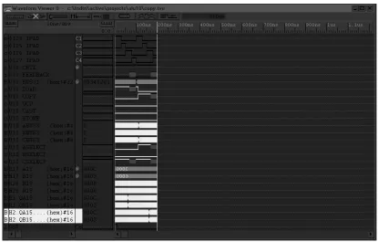
3.1.8 Copy Circuit
[image:43.595.139.554.132.397.2]The Copy circuit is part of the Simulation 1 (Appendix B.3). It copies contents of one register into another.
Figure 26. Copy Simulation.
3.1.9 Move Circuit
[image:44.595.140.553.174.541.2]The Move Circuit is part of Simulations 4 and 5 (Appendix B.6 and B.7). It moves the denominator from one register and puts it into the numerator and denominator of another register. This is then used in conjunction with Add Circuit to make the denominators the same for both numbers.
Figure 27. Move Simulation
3.2 Register Unit
3.2.1 32-bit Register Circuit
[image:45.595.140.555.214.571.2]The 32-bit Registers store data from the CAU. The registers are enabled using Control Unit (Section 3.3) and the third clock sub-cycle. All operations of the CAU use registers, plus LOAD and STORE operations.
Figure 28. 32-bit Register Simulation.
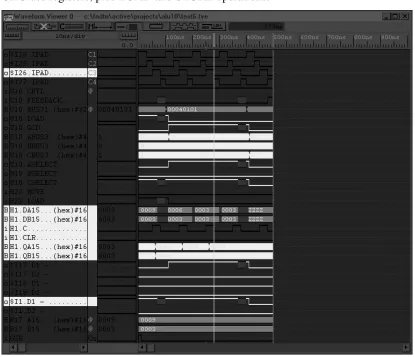
3.2.2 Register Address Decoding Circuit
Register Address Decoding Circuit allows selecting right registers for input and output. For A and B Bus the decoding enables or disables Tristate Buffers and for
[image:46.595.141.555.150.504.2]C bus the decoding enables or disables registers.
Figure 29. Register Address Decoding Simulation.
This simulation is during GCD operation. Register numbers are selected using U10.ABUS3, U10.BBUS3 and U10.CBUS3 signals. In this case ABUS and CBUS are set to 1, which means GCD will receive data from Register R1 and will store results into R1. $I17.D1 is High indicating that Tristate Buffer for A bus
3.3 Control Unit
3.3.1 Operations Decoding Circuit
[image:47.595.140.553.202.547.2]Operations Decoding Circuit allows the Control Unit to interpret the Control Word and enable a specific operation.
Figure 30. Operations Decoding Simulation.
3.3.2 Register Selection Circuit
[image:48.595.141.553.132.485.2]Register Selection Circuit interprets the Control Word and enables the right set of registers for the given operation.
Figure 31. Register Selection Simulation.
3.3.3 Feedback Unit
[image:49.595.141.555.148.503.2]The Feedback Unit informs the Control Unit about completion of a specific operation. The END line from all circuits goes to the Feedback Unit, where they are processed and a single line is sent back to the Control Unit.
Figure 32. Feedback Simulation.
3.4 Input/Output Interface Unit
3.4.1 Parallel Port Interface
No simulations have been performed for this unit. When it became apparent that the FPGA device will not be obtained on time, main effort was put on fine tuning the arithmetic circuits. While this circuit works when tested independently, it has several timing problems when integrated with the rest of the device. Also the design of output to the parallel port wasn’ t accomplished. However this circuit can give some idea to future researchers on how to do the interfacing with PC. Help on this topic was very hard to obtain and this circuit may be of help.
3.4.2 Load Circuit
[image:50.595.141.555.402.670.2]The Load Circuit is part of all Simulations in Appendix B but the most detail is provided in Simulation 1 (Appendix B.3). The circuit allows receiving data from the parallel port and putting it in one of the registers.
Figure 33. Load Simulation.
3.4.3 Store Circuit
[image:51.595.142.553.201.467.2]The Store Circuit is part of all Simulations in Appendix B but the most detail is provided in Simulation 1 (Appendix B.3). The circuit allows receiving data from a register and sending it to the parallel port.
Figure 34. Store Simulation.
4.1 Results
The results obtained suggest that the design of the arithmetic circuits is correct. The most important thing however is controlling the end of operation, especially for circuits like MUL, GCD and CAST. Biggest difficulties were with combining the Control Unit with the Interface Unit and handling of feedback loops. Also timing for the whole circuit had to be changed frequently to achieve the best sequence for the events. The difficulty with obtaining the FPGA device forced to delay the implementation significantly and in the end it could not be carried out. It also delayed the design of the Interface Unit, which works independently, but it has several timing faults that prevented it from final integration with the rest of the device. The implementation of the device could be part of another project or results of this thesis could be incorporated in a further study on exact forms.
4.2 Relevance of the Thesis
The thesis is the first type of research in this field. While the proposal for Composite Arithmetic has been published (Holmes, 1997a), work is required to implement and test the concept. The project dealt with exact forms of the Composite Arithmetic. Integer numbers are special case of rational number with denominator 1. This was done to fit integers into the scope of the project. The thesis will form a base for investigating the exact forms. The circuits completed can be easily incorporated into other designs and control process will serve as an example of how to control the CAU. A paper has also been submitted to IEEE conference (2000 IEEE SoutheastCon) in Nashville, Tennessee, USA, in hope of introducing the concept to other researchers, and getting some feedback and help on this topic. Successful submission could result in creating new projects in the field of computer arithmetic and could benefit to the University of Tasmania.
4.3 Further Research
from the exact part of the CAU. Once the CAU is designed memory storage and display issues will need to be solved. This will require memory management device and software driver that will transform the data from register form into appropriate display form. Only then the system will be fully capable of performing Composite
References
Holmes, N. “Composite Arithmetic: Proposal for a New Standard.” IEEE Computer, 1997a,
65-73
Holmes, N. “Floating Point and Composite Arithmetic.” Proceedings, 8th Biennial
Computational Techniques and Applications Conference, 1997b
Hwang, K., 1979, Computer Arithmetic: Principles, architecture and design, John Wiley &
Sons
Kulisch, U.W. Advanced Arithmetic for the Digital Computer – Design of Arithmetic Units,
Version 2, 1999
Tanenbaum, A.S., 1990, Structured Computer Organisation, 3rd Edition, Prentice Hall, New
Jersey
Villasenor, J., Mangione-Smith, W.H. “Configurable Computing.” Scientific American, 1997,
Appendix A: Simple Composite Arithmetic
Machine
Figure 35. SCAM Diagram showing main components.
Main Components: Composite Arithmetic Unit Control Unit
Register Unit Feedback Unit Interface Unit
Other Components: Bus Latches
Appendix B: Simulations
1. CONTROL WORD
Control Word provides 32-bit data to the SCAM device about the next instruction to be executed. The higher 16 bits represent the opcode of the operation to be carried out. In fact higher 8 bits are always 0 and only lower 8 bits are used. The lower 16 bits of the control word tell which register is to be used. Starting from the highest nibble down, the first nibble is always zero, the second nibble denotes the C Bus, then third and fourth is for B Bus and A Bus respectively.
Operation OPCODE Registers Comment
NOP 0000 0000
GCD 0004 0X0X Get contents of X and put it back into X CAST 0008 0XYX Get contents of X and Y and put it back into X SWAP 000C 0X0X Get contents of X and put it back into X MUL 0010 0XYZ Multiply Z by Y and put result into X
DIV Done using SWAP and MUL operations
ADD 0018 0XYZ Add Z to Y and put result into X SUB 001C 0XYZ Subtract Z from Y and put result into X MOVE 0030 0X0Y Get contents of Y and put it back into X COPY 0034 0X0Y Get contents of Y and put it back into X LOAD 0038 0X00 Put data into X
STORE 003C 000X Get contents of X
2. CLOCK SIMULATION SEQUENCE: Nil
INPUTS: Nil
OUTPUTS:
$I28.IPAD – Clock 1 $I25.IPAD – Clock 2 $I26.IPAD – Clock 3 $I27.IPAD – Clock 4
TEST DATA IN: Nil
TEST DATA OUT: Nil
Figure 36. Clock Simulation. Clock Timings:
Clock 1 – 25ns High, 75ns Low
Clock 2 – 25ns Low, 25ns High, 50ns Low Clock 3 – 50ns Low, 25ns High, 25ns Low Clock 4 – 75ns Low, 25ns High
Clock Functions:
Clock 1 – Operates the latches that latch outputs from the Register Unit. Clock 2 – Provides clock cycle for the Composite Arithmetic Unit. Clock 3 – Provides clock cycle for the Register Unit.
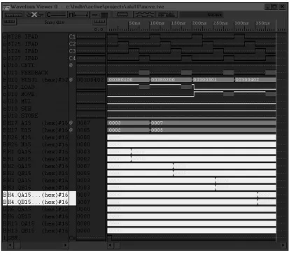
3. SIMULATION ONE – GCD AND CAST
SEQUENCE: Load R1, Copy R1 to R2, GCD R2, Cast R1 and R2 to R1, Store R1
INPUTS:
U10.CNTL – Control Signal from I/O Interface
U10.FEEDBACK – Feedback signal from the Feedback Unit U10.BUS31 – Control Word
H17.A15 – Denominator of the input number H17.B15 – Numerator if the input number
OUTPUTS:
$I28.IPAD – Clock 1 $I25.IPAD – Clock 2 $I26.IPAD – Clock 3 $I27.IPAD – Clock 4
U10.LOAD – Line enabling Load operation U10.COPY – Line enabling Copy operation U10.GCD – Line enabling GCD operation U10.CAST – Line enabling Cast operation U10.STORE – Line enabling Store operation U10.ABUS3 – Register number on A bus U10.BBUS3 – Register number on B bus U10.CBUS3 – Register number on C bus U10.ASELECT – Select line for A bus U10.BESLECT – Select line for B bus U10.CSELECT – Select line for C bus H26.M15 – Denominator of the output number H26.N15 – Numerator of the output number H1.QA15 – Denominator output of the Register R1 H1.QB15 –Numerator output of the Register R1 H2.QA15 – Denominator output of the Register R2 H2.QB15 – Numerator output of the Register R2
TEST DATA IN: Rational Number 3/12
[image:57.595.136.545.476.735.2]TEST DATA OUT: Rational Number: 1/4
4. SIMULATION TWO – MUL
SEQUENCE: Load R1, Load R2, Mul R1 and R2 to R3, Store R3
INPUTS:
U10.CNTL – Control Signal from I/O Interface
U10.FEEDBACK – Feedback signal from the Feedback Unit U10.BUS31 – Control Word
H17.A15 – Denominator of the input number H17.B15 – Numerator if the input number
OUTPUTS:
$I28.IPAD – Clock 1 $I25.IPAD – Clock 2 $I26.IPAD – Clock 3 $I27.IPAD – Clock 4
U10.LOAD – Line enabling Load operation U10.MUL – Line enabling Multiply operation U10.STORE – Line enabling Store operation H26.M15 – Denominator of the output number H26.N15 – Numerator of the output number H1.QA15 – Denominator output of the Register R1 H1.QB15 –Numerator output of the Register R1 H2.QA15 – Denominator output of the Register R2 H2.QB15 – Numerator output of the Register R2 H3.QA15 – Denominator output of the Register R3 H3.QB15 – Numerator output of the Register R3
TEST DATA IN: Rational Number: 3/2 Rational Number: 7/5
TEST DATA OUT:
[image:58.595.135.546.402.636.2]Rational Number: 21/10 (15/0A in Hex)
5. SIMULATION THREE – DIV
SEQUENCE: Load R1, Load R2, Swap R2, Mul R1 and R2 to R3, Store R3
INPUTS:
U10.CNTL – Control Signal from I/O Interface
U10.FEEDBACK – Feedback signal from the Feedback Unit U10.BUS31 – Control Word
H17.A15 – Denominator of the input number H17.B15 – Numerator if the input number
OUTPUTS:
$I28.IPAD – Clock 1 $I25.IPAD – Clock 2 $I26.IPAD – Clock 3 $I27.IPAD – Clock 4
U10.SWAP – Line enabling Swap operation U10.MUL – Line enabling Multiply operation H26.M15 – Denominator of the output number H26.N15 – Numerator of the output number H1.QA15 – Denominator output of the Register R1 H1.QB15 –Numerator output of the Register R1 H2.QA15 – Denominator output of the Register R2 H2.QB15 – Numerator output of the Register R2 H3.QA15 – Denominator output of the Register R3 H3.QB15 – Numerator output of the Register R3
TEST DATA IN: Rational Number: 3/2 Rational Number: 7/5
TEST DATA OUT:
[image:59.595.131.548.402.625.2]Rational Number: 15/14 (0F/0E in Hex)
6. SIMULATION FOUR – ADD
SEQUENCE: Load R1, Load R2, Move R1 to R3, Move R2 to R4, Mul R1 and R4 to R12, Mul R2 and R3 to R13, Add R12 and R13 to R1, Store R1
INPUTS:
U10.CNTL – Control Signal from I/O Interface
U10.FEEDBACK – Feedback signal from the Feedback Unit U10.BUS31 – Control Word
H17.A15 – Denominator of the input number H17.B15 – Numerator if the input number
OUTPUTS:
$I28.IPAD – Clock 1 $I25.IPAD – Clock 2 $I26.IPAD – Clock 3 $I27.IPAD – Clock 4
U10.LOAD – Line enabling Load operation U10.MOVE – Line enabling Move operation U10.MUL – Line enabling Multiply operation U10.ADD – Line enabling Add operation U10.STORE – Line enabling Store operation H26.M15 – Denominator of the output number H26.N15 – Numerator of the output number H1.QA15 – Denominator output of the Register R1 H1.QB15 –Numerator output of the Register R1 H2.QA15 – Denominator output of the Register R2 H2.QB15 – Numerator output of the Register R2 H3.QA15 – Denominator output of the Register R3 H3.QB15 – Numerator output of the Register R3 H4.QA15 – Denominator output of the Register R4 H4.QB15 – Numerator output of the Register R4 H6.QA15 – Denominator output of the Register R12 H6.QB15 – Numerator output of the Register R12 H13.QA15 – Denominator output of the Register R13 H13.QB15 – Numerator output of the Register R13
TEST DATA IN: Rational Number: 2/3 Rational Number: 5/7
TEST DATA OUT:
7. SIMULATION FIVE – SUB
SEQUENCE: Load R1, Load R2, Move R1 to R3, Move R2 to R4, Mul R1 and R4 to R12, Mul R2 and R3 to R13, Sub R13 from R12 to R1, Store R1
INPUTS:
U10.CNTL – Control Signal from I/O Interface
U10.FEEDBACK – Feedback signal from the Feedback Unit U10.BUS31 – Control Word
H17.A15 – Denominator of the input number H17.B15 – Numerator if the input number
OUTPUTS:
$I28.IPAD – Clock 1 $I25.IPAD – Clock 2 $I26.IPAD – Clock 3 $I27.IPAD – Clock 4
U10.LOAD – Line enabling Load operation U10.MOVE – Line enabling Move operation U10.MUL – Line enabling Multiply operation U10.SUB – Line enabling Sub operation U10.STORE – Line enabling Store operation H26.M15 – Denominator of the output number H26.N15 – Numerator of the output number H1.QA15 – Denominator output of the Register R1 H1.QB15 –Numerator output of the Register R1 H2.QA15 – Denominator output of the Register R2 H2.QB15 – Numerator output of the Register R2 H3.QA15 – Denominator output of the Register R3 H3.QB15 – Numerator output of the Register R3 H4.QA15 – Denominator output of the Register R4 H4.QB15 – Numerator output of the Register R4 H6.QA15 – Denominator output of the Register R12 H6.QB15 – Numerator output of the Register R12 H13.QA15 – Denominator output of the Register R13 H13.QB15 – Numerator output of the Register R13
TEST DATA IN: Rational Number: 7/5 Rational Number: 3/2
TEST DATA OUT:
Appendix C: LogiBLOX Modules
1. AN8
Function: Provides Logical AND operation of 8-bit input. Type: Simple Gates (Type 1)
[image:64.595.142.520.148.445.2]Gate Type: AND Bus width: 8 bits
2. AN16
Function: Provides Logical AND operation between 16-bit input and 1-bit input. Type: Simple Gates (Type 2)
[image:65.595.144.519.134.440.2]Gate Type: AND Bus width: 16 bits
3. AN32
Function: Provides Logical AND operation between 32-bit input and 1-bit input. Type: Simple Gates (Type 2)
[image:66.595.142.518.132.438.2]Gate Type: AND Bus width: 32 bits
4. BUF2
Function: Provides buffering for 2-bit input. Type: Inputs/Outputs
IO Type = Output
[image:67.595.139.521.126.504.2]Output operation = Buffer Only Bus width: 2 bits
5. BUF4
Function: Provides buffering for 4-bit input. Type: Inputs/Outputs
IO Type = Output
[image:68.595.139.521.125.505.2]Output operation = Buffer Only Bus width: 4 bits
6. BUFFER16
Function: Provides tristate buffering for 16-bit input. Type: Tristate Buffers
[image:69.595.136.519.119.341.2]Bus width: 16 bits
Figure 47. BUFFER16 LogiBLOX Module. 7. COMPARE16
Function: Compares two 16-bit inputs A and B and returns three lines: A equals B, A is less than B and A is greater than B. These are set according to the result of comparison to High or Low. Type: Comparators
Operations: A = B, A < B, A > B Bus width: 16 bits
[image:69.595.142.519.415.680.2]8. EQUAL16
Function: Compares two 16-bit inputs A and B and returns one line: A equals B. It is set according to the result of comparison to High or Low.
[image:70.595.140.519.130.413.2]Type: Comparators Operations: A = B Bus width: 16 bits
9. O16
Function: Provides Logical OR operation of two 16-bit inputs. Type: Simple Gates (Type 3)
[image:71.595.138.520.124.436.2]Gate Type: OR Bus width: 16 bits
10. SELECTOR16
Function: Multiplexes two 16-bit inputs depending on the value of the control line. Type: Multiplexers (Type 2)
[image:72.595.142.519.132.443.2]Input Buses: 2 Bus width: 16 bits
11. SHIFTREG16
Function: Provides a Logical 16-bit Right Shift Register, with MSB Input and MSB, LSB output Type: Shift Registers
Shift Operation: Right Shift Type: Logical Inputs: MSB Serial
Outputs MSB Serial, LSB Serial
[image:73.595.140.519.158.524.2]Control: Asynchronous with Clock Enable Bus width: 16 bits
3
32-bit Register Circuit...21
A Add Circuit...16
Application-Specific Integrated Circuits...5
C Casting Circuit...11
Composite Arithmetic...3
Composite Arithmetic Unit...9
Configurable Computing ...See FPGAs Configurable Logic Blocks ...6
Control Unit ...23
Control Word ...23
Copy Circuit...18
D display form ...4
Divide Circuit...16
E Euclid’ s Algorithm ...10
exact forms...3
F Feedback Unit...26
Field Programmable Gate Arrays ...5
Fixed-point...1
Floating-point...1
G Greatest Common Divisor Circuit...10
I inexact forms...4
integer form...See exact forms L Load Circuit...28
long accumulator...5
M Move Circuit...19
Multiplication (Hwang’ s algorithm) ...15
Multiply Circuit...15
O Operations Decoding Circuit...25
overflow ...See Floating-point arithmetic P Parallel Port Interface...27
R rational form...See exact forms Register Address Decoding Circuit...22
register form...5
Register Selection Circuit...25
Register Unit ...20
S Scalar product ...2
Store Circuit...29
Subtract Circuit...17
Swap Circuit...14
U

![Figure 4. Cast Circuit casts out common factors of two 16-bit numbers. Three data inputs are A [15:0] (denominator), B [15:0] (numerator) and GCD [15:0] (GCD of A and B calculated earlier)](https://thumb-us.123doks.com/thumbv2/123dok_us/8463195.338724/19.595.140.554.70.463/figure-circuit-factors-numbers-denominator-numerator-calculated-earlier.webp)