1-1-1986
A data acquisition system design based on a
single-board computer
Tou-Chung Hou
Iowa State University
Follow this and additional works at:https://lib.dr.iastate.edu/rtd Part of theEngineering Commons
This Thesis is brought to you for free and open access by the Iowa State University Capstones, Theses and Dissertations at Iowa State University Digital Repository. It has been accepted for inclusion in Retrospective Theses and Dissertations by an authorized administrator of Iowa State University Digital Repository. For more information, please [email protected].
Recommended Citation
Hou, Tou-Chung, "A data acquisition system design based on a single-board computer" (1986).Retrospective Theses and Dissertations. 18236.
.::£-SlL
I
qg
(o1-1
'81
c. ,3
Approved:
by
Tou-Chung Hou
A Thesis Submitted to the
Graduate Faculty in Partial Fulfillment of the Requirements for the Degree of
MASTER OF SCIENCE
In terdepar tmen tal Program:
Major: Biomedical Engineering Biomedical Engineering
Signatures have been redacted for privacy
Iowa State University Ames, Iowa
TABLE OF CONTENTS
INTRODUCTION LITERATURE REVIEW
DISCUSSION OF SINGLE-CHIP BASIC MICROCOMPUTERS Introducing the MC-lZ
The Z8671 MCU The 8255A PPI
The MM58274 real-time clock/calendar The serial interface buffers
Additional I/O lines
A BLOCK DIAGRAM OVERVIEW THE ZS DATA ACQUISITION SYSTEM Subsystems
A/D D/A
Solid-state relays
Electromechanical relays The sense switches
The keypad
System device control
SOFTWARE DEMONSTRATION OF CAPABILITIES A Program to Count .Heart Rate
CONCLUSION BIBLIOGRAPHY ACKNOWLEDGEMENTS
APPENDIX: MANUFACTURERS OF SINGLE-BOARD 'BASIC' COMPUTERS
INTRODUCTION
Over the past four decades the computer ind.us try .has experienced four generations of development, physically marked by rapid changes of building blocks from relays and vacuum tubes (1940-1950s), to discrete diodes and transistors (1950-1960s), to small- and medium-scale
in-tegrated circuits {SSI/MSI) (1960-1970s.), and to large- and
very-large-scale integrated circuits (LSI/VLSI) (1970s and beyond). In-creases in device speed and reliability and reduction in hardware cost and physical size have greatly enhanced computer performance.
Computers are increasingly in demand in the area of structural analysis, weather forecasting, petroleum exploration, fusion energy research, medical diagnosis, aerodynamics simulation, artificial intel-ligence, expert system, industrial automation, remote sensing, military defense, genetic engineering, socioeconomics, and other scientific and engineering applictions. They are used almost everywhere. They are un-deniably becoming more and more important in human lives,
LITERATURE REVIEW
New industrial, commercial, and consumer products containing
microcomputers are announced almost daily, Many manufacturers are apply-ing microcomputer technology to their products to increase versatility, simplify operation, reduce cost or improve reliability, A similar trend is occurring in the medical device industry. Laboratory automation, data acquisition from analytical instruments, and patient monitoring are.but a few of areas benefiting from the microcomputer.
In medical usage, an Intel 8748 microcomputer was used to build a computer-based system to help a handicapped (quadriplegic) computer pro-grammer (Ramey et al,, 1982). A Motorola 6800 microprocessor was used to construct a computer-based system for the disabled (Bolton and Taylor, 1981). This system used breath-powered signals to help a tetraplegic select characters for a typewriter. It could also link to another com-puter directly or to a modem for transmission of data via a telephone line. A commercial (Datel) data acquisition system was modified for electrophysiological application (Demjanenko and Sachs, 1982). The Datel
ST series lacked a programmable sampling clock and a multichannel sample and hold. Both of these features are often vital to biophysical experi-ments where it is necessary to sample at precise intervals and/or change
the sampling rate during an experiment. This system added a programmable interval timer and a sample and hold unit to the Datel ST unit, making it more adaptable for biophysical experiments than the original device. A 6802 central processing unit (CPU) was used to construct a
procedure time was greatly reduced, taking ·only a few seconds for data acquisition. There was no need for baseline centering, lead switching, or amplifier setting. The requirements for cable and amplifier shielding and electrode/skin contact were greatly reduced too. The use of a fast microdot printer/plotter eliminated the problem of mechanical fragility .of the recording system and greatly reduced the need for servicing. A
single-board computer (SBC S0/24) was used to build a computer-based sys-tem for the measurement and analysis of an expiratory flow-control curve (El-Dhaher ~t al., 19S3).
A ZS BASIC system controller was used to build a computer-based com-munication aids to help the vocally handicapped (Rolander, 19S4). A
smal·l keyboard was used as an input device to the ZS BASIC controller. The processed signal was then sent to two speech synthesizers to produce
the desired words or phrases. The processed signal could also be sent to a liquid crystal display to show the words or phrases. This device was easy to operate.
Comparing the above examples, it can be seen that there are dif-ferent purposes, usages, and design schemes. But some common design cri-teria are evident:
1. The cost of the system is low.
2. The reliability of the system is high. 3. The performance of the system must be high.
-6. The system is light in weight and small in size.
7. The system needs less power for operation.
Many times, the computer-based system can't meet all the criteria. Then we must consider which one is the most important, which one is the second most important, ••• ,e.tc. Later, we use our priorities in designing the computer-based system. For example, a computer-based automatic con-trol system in an airplane must have very high reliability, even though the price is high. The high price compensates the high reliability.
Sometimes designing a computer-based system for a special purpose becomes too complex. This project describes a data acquisition system design us-ing a sus-ingle-board computer. Some general design ideas for a
DISCUSSION OF SINGLE-CHIP BASIC MICROCOMPUTERS
There are three single-chip BASIC microcomputers (MCUs) - Zilog Z8671, National Semiconductor (N.S.C.) INS8073, and Intel 8052AH-BASIC. The ,addresses of 13 manufacturers which use these single-chip BASIC MCUs in their single-board computers are presented in the Appendix.
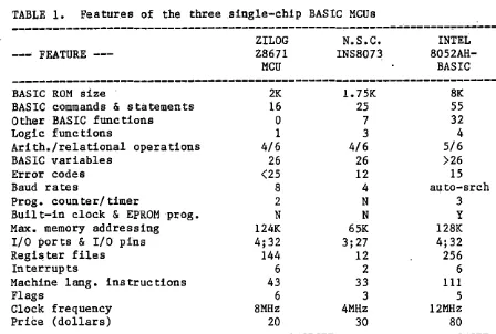
All three of the MCUs have these features: auto-startup with user's ROM; on-board universal asychronous receiver/transmitter (UART); can call machine language subroutines to increase execution speed; +5 V supply voltage; input/output (I/O) pins are transistor-transistor-logic (TTL) compatible; direct. access to register and memory locations; can use both hexadecimal and decimal numbers; line editor (interactive debug program); can support memory-mapped I/O; on-chip oscillator; and a 40-pin package. A comparison of the three MCQs is given in Table 1.
If the different features of the three MCUs are compared, you will note that the N.S.C. INS8073 appears to be the lowest in performance. National Semiconductor Corporation has ceased production of the INS8073. The Intel 8052AH-BASIC MCU is superior to the Zilog Z8671. There are four advantages of the Z8671 MCU and were the reasons for its choice. 1. Low cost - about $20; the price of the Intel 8052AH-BASIC is
approximately $80.
2. It is an established product and is described by a lot of d<icumen ta tion.
TABLE !. Features of the three single-chip BASIC MCUs
--- FEATURE --- ZILOG Z8671
MCU
N.S.C.
INS8073 8052AH-INTEL BASIC
---BASIC ROM sizeBASIC commands & statements Other BASIC functions
Logic functions
Ari th. /relational operations BASIC variables
Error codes Baud rates
Prog. counter/ timer
Built-in clock
&
EPROM prog. Max. memory addressingI/O ports
&
I/O pins Register filesInterrupts
Machine lang. instructions Flags
Clock frequency Price (dollars)
2K 16 0 1 4/6 26 <25 8 2 N 124K 4;32 144 6 43 6 SMHz 20
!. 75K
25 7 3 4/6 26 12 4 N N 65K 3; 27 12 2 33 3 4MHz 30 SK 55 32 4 5/6 >26 15 au.to-srch 3 y 128K 4;32 256 6 111 5 12MHz 80
4. The author is more familiar with it than with the Intel.MCU.
Introducing the MC-lZ
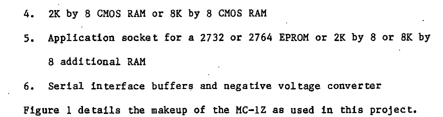
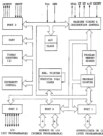
The MC-lZ is a single-board computer that can be used in "real-time" control applies tions. It is manufactured by Basic on Corporation and costs approximately $160. It is compact, easy to use and affords a variety of applications through its 40 I/O lines. It contains the fol-lowing major components:
1. Z8671 MCU with resident tiny BASIC
[image:9.572.65.513.68.370.2]4. 2K by B CMOS RAM or BK by B CMOS RAM
5. Application socket for a 2732 or 2764 EPROM or 2K by B or BK by B additional RAM
6. Serial interface buffers and negative voltage converter
Figure 1 details the makeup of the MC-lZ as used in this project. A memory map of the MC-lZ is shown in Figure 2.
The ZB671 MCU
The ZB671 MCU is an B-bit MCU. It has a BASIC/DEBUG interpreter in ROM. Because the BASIC/DEBUG interpreter is present in the ZB671 MCU, programming is made much easier. The ZB671 MCU allows fast hardware tests, and bit-by-bit examination of any memory location, I/O port, or register. It also allows bit manipulation and logical operations. It has a self-contained line editor to support interactive debugging, further speeding up program development.
[image:10.571.81.524.67.184.2]-:5V
' I
-5
v
1 PORTSCONV Z8671 I I 2 & 3 / { 14 I/OJ
"'
I v
-RESET
-
CKT.'
RS232 BUFFER
>----
8255 PPI A ~/ (24 I/O)
v
2K/8K BATT.
RAM
'
CR'l! 4K/8K
EPROM ·
'
CLOCK/ CAL.
[image:11.574.75.404.68.644.2]HEX. ADDR.
FFFD
I
BAUD RATE SELECTBS03
I
S255A P.P.I. BSOOCLOCK/CALENDAR ASOF
I
ASOO 1... ----~---'
4FFF ZS VARIABLES - 1/4 K
lFFF
07FF
---RAM
4K EPROM
~ AUTO START AT 1020
ZS BASIC
&
REGISTERS
FIGURE 2. The MC-lZ MCU memory map
SIZE (BYTES)
1
4
16
SK
EXP. TO SK
[image:12.571.63.406.64.710.2]OUTPUT INPUT Vee GND
•
'
"
PORT 3
"1--
1/
UART
/l--
ALU'
"'
---
FLAGSTIMER/
/I-COUNTERS
'y---( 2)
REG. POINTER
..._
1-.---
REGISTER FILEINTERRUPT I/~ 124X8
I.-CONTROL
~
~">-~7
~5
/1-PORT 2
•
1
I/O(BIT PROGRAMMABLE)
PORT 0
,/\.
,/4 4
\/"'
ADDRESS OR I/O (NIBBLE PROGRAMMABLE)
XTAL AS DS R/W RESET
MACHINE TIMING
&
INSTRUCTION CONTROL
/~
PROGRAM MEMORY 2048X8
,('/
I PROGRAM
COUNTER
1
'\ /'7
~
PORT 1v
8
v
ADDRESS/DATA OR I/O (BYTE PROGRAMMABLE)
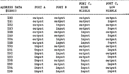
[image:13.571.62.477.80.627.2]The 8255A PPI
The 8255A PPI is a general-purpose I/O interfacing device. It provides 24 I/O lines organized as three 8-bit I/O ports"labeled A, B, and
c.
All of the bits in ports A or B are programmed as one byte. The four high- and four low-order bits of port C can be programmed as two separate nibbles.The 8255A PPI is a very versatile device. It can be programmed to look like three simple I/O ports (mode O), two handshaking I/O ports (mode 1), or a bidirectional I/O port with five handshaking signals (mode 2). The modes can also be intermixed. For example, port A.can be pro-grammed to operate in mode 2, while port B operates in mode O. There is also a bit set/reset mode that allows individual bits of port C to be set or reset for control purposes.
The 82'55A PPI occupies four sequential memory locations in the MC-lZ:
%B800 %B801 %B802
%B803
port A port B port C
PPI control register
D7 D6 DS D4 D3 D2 Dl DO
X=O OUTPUT X=l INPUT
FIGURE 4. The control register used to program the inputs and outputs of the 8255A PP! in mode 0
TABLE 2. The 16 combinations for the inputs and outputs of ports A, B, and C
ADDRESS DATA
@%B803 %80 %81 %82 %83 %88 %89 %8A %SB %90 %91 %92 %93 %98 %99 %9A %9B
PORT A
OU tput OU tput
output
OU tput OU tput
output
OU tput
output input input input input input input input input
PORT B
OU tput OU tpu t
input input output output input input
OU tput OU tput
input input
OU tput
output input input
PORT C,
HIGH NIBBLE
OU tpu t OU tpu t OU tput OU tput
input input input input output output output output input input input input
PORT C., LOW NIBBLE
OU tput
input output input output input output input output input output input output input output input
Each time the 8255A PP! is reset, all of the ports are configured as
inputs and the lines are floa.ting. Each time the 8255A PPI- control
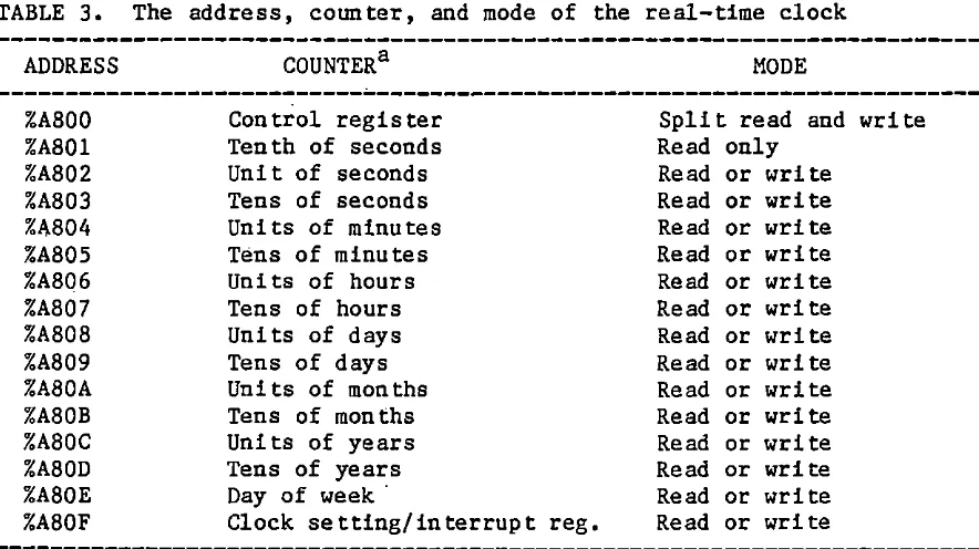
[image:15.569.72.517.31.604.2] [image:15.569.74.512.335.587.2]The MM58274 real-time clock/calendar
The MC-lZ has a real-time clock/calendar. The clock/calendar is an N.s.c. MM58274 which provides tenths of seconds through years, including leap year calculation. The clock is crystal controlled and requires low power. In the MC-lZ the real time clock resides in memory locations %A800 thru %A80F as shown in Table 3.
TABLE 3. The address, counter, and mode of the real-time clock
ADDRESS COUNTER a MODE
---~---%A800 Control register Split read and write
%A801 Tenth of seconds Read only
%A802 Unit of seconds Read or write
%A803 Tens of seconds Read or write
%1\804 Units of minutes Read or write
%A805 Tens of minutes Read or write
%A806 Units of hours Read or write
%A807 Tens of hours Read or write
%A808 Uni ts of days Read or write
%A809 Tens of days Read or write
%A80A Uni ts of months Read or write
%A80B Tens of months Read or write
%A80C Uni ts of years Read or write
%A80D Tens of years Read or write
%A80E Day of week· Read or write
%A80F Clock set ting/ interrupt reg. Read or write
---a All coµnters are four bit counters and utilize the lower four bits of the data bus (DO-D3).
The clock must be initialized after power up. During initializa-tion, the clock is stopped and the interrupts are disabled by setting the control register to 5, @%A800=5. The hour setting can be specified for either 12 or 24 hour mode. If 12 hour mode is selected:
If am:
[image:16.570.70.512.242.490.2]@%A80F=4 If this year is a leap year plus one year. @%A80F=8 If this year is a leap year plus two years.
@%A80F=l2 If this year is a leap year plus three years.
If pm:
@%A80F=2 If this year is a leap year.
@%A80F=6 If this year is a leap year plus one year. @%A80F=l0 If this year is a leap year plus two years. @%A80F=l4 If this year is a leap year plus three years. If 24 hour mode is selected:
@%A80F=l If this year is a leap year.
@%P,80F=5 If this year is a leap year plus one year. @%A80F=9 If this year is a leap year plus two years. @%A80F=l3 If this year is a leap year plus three years. Finally the clock is set by loading memory locations %A802 through %ABOF with desired data. For example, to set 1:47:42 pm on July 15, 1986 (12 hour mode):
@%A802=2
?The seconds @%A803=4
@%A804=7
~The
minutes~%A805=4
@%A806=1
~The
hours @%A807=0@%A808=5
~Day
of the month @%A809=1@%A80A=7
@%A80C=6 ---~
~The
year@%A80D=8
---~-@%A80E=3 Tuesday, the third day of the week
@%A80F=l0 This is a leap year plus two years.
It is.conventional to assign Sunday as the first day of the week.
So, Tuesday is the third day of the week.
When everything is set the clock is started with either of two
commands: @%A800=0 (interrupt timer is running) or @%A800=1 (interrupt
timer is off). The clock is stopped with a @%A800=4 command.
The serial interface buffers
There are two serial interface buffers (RS232/TTL and TTL/RS232
con-version) in the MC-lZ. RS232 was developed in the early 1960s as a
stan-dard governing the interconn~ction of terminals and modems. The RS232
standard defines a single-ended transmission technique limited to 20,000
baud with a 50-ft cable. The conversion buffers and the Z8671's UART use
3 lines (transmitted data, received data, and signal ground) to connect
to a terminal.
The most striking feature about RS232 is that the logical levels are
n_ot TTL-compatible. TTL is fine for short-distance cables of 5 to 10 ft,
provided that the ·data rate is not too high. However, as the cable
length increases, the capacitive and DC loading effects reduce the noise
margins_ to unacceptable levels.
An RS232 receiver will interpret a voltage more negative than -3 V
as a logic 1 and a voltage more positive than +3 V as a logic O. RS232
for logic 1 and more positive than +5 V for a logic
o.
The actual output voltage depends on the supply voltages used. With this scheme 2 V of noise immunity is guaranteed. This should be compared with Q.4 V for standard TTL. The conversion buffers are placed be tween the RS232 lines and the UART to assure that terminal-computer communication can occur.Additional I/O lines
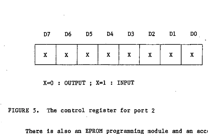
The MC-lZ still has 14 I/O lines which come directly from the Z8671 MCU. They are assigned as port 2 and port 3. Eight of the 14 lines be-long to port 2, the others bebe-long to port 3. The control registers for ports 2 and 3 are registers .246 and 247, respectively. The control word for port 3 is complex and does not need to be illustrated here. The ma-jority of uses will define P3(1) to P3(3) as simple inputs and P3(4) to P3(6) as simple outputs. The command for this is @247=%41. P3(0) (input) and P3( 7) ( output) are comm! tted to serial I/O with a terminal.
The control register for port 2 is register 246. A control word is sent to 246 to set what bits of port 2 are inputs and outputs. Figure 5 shows how to set the inputs and outputs of port 2.
For example: @246=0 @246=%F @246=%FO @246=%FF
All lines are output lines.
D7 D6 DS D4 D3 D2 Dl DO
x
x
x
x
x
x
x
x
X=O OUTPUT X=l INPUT
FIGURE S. The control register for port 2
There is also an EPROM programming module and an accompanying
utility PROM (ZUTIL-1.00) to support the MC~lZ. The utility PROM offers
fourteen commands for program development on the MC-lZ. These fourteen commands are divided into five groups:
1. Alter memory and check memory: Alter memory (A), Copy memory (C), Display memory (D), and Fill memory (F).
2. Copy a program inside RAM to EPROM: Erase check (E), Program EPROM (P), and Verify EPROM (V).
3. Copy a program inside EPROM to RAM: Display ROM (R)_and Copy ROM to memory (G).
4. Mark the top of a program ·and find the end of a program: Mark top (M) and Locate data (L).
5. Accessory: Help (H), Set time (S), and Time check (T).
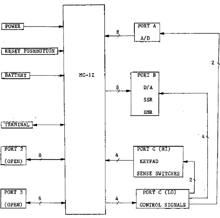
[image:20.570.59.421.58.292.2]A BLOCK DIAGRAM OVERVIEW THE ZS DATA ACQUISITION SYSTEM
The Basicon MC-lZ single-board computer was used as the main part of the ZB data acquisition system, Its 24 parallel programmable I/O lines which come from the 8255A PPI were connected to the A/D converter, D/A drivers, relay drivers, sense switches, and a keypad.
In this system, port A was configured as an input port for the A/D converter, port B was configured as an output port for the two D/A verters, relay drivers (and relays). The high nibble of port C was con-figured as input lines for the sense switches and the keypad and the low nibble of port C was configured as output lines to a 4-to-16 decoder. The decoder output lines are the control lines for the ZB data
acquisi-tion system •. A block diagram of the system is shown in Figure 6. The advantages of this system are the following.
1. It only needs one ( +5 V) power supply for operation. 2. It is light in weight and compact to carry.
3·, The system can be reset wi.th a pushbutton without losing your application program.
4. A battery will keep the RAM and real-time clock/calendar alive, 5. The utility PROM (ZUTIL-1.00) (a 2732 EPROM installed in the
POWER PORT A 8
A/D RE_SET PUSHBUTTON
1--2 '
BATTERY, MC-lZ PORT B
8 D/A
SSR EMR TERMINAL
. 4.
PORT 2 PORT C (HI)
8 4
(OPEN) , KEYPAD ~
SENSE SWITCHES
z,
PORT 3 PORT C (LO)
>--6 4
(OPEN) CONTROL SIGNALS
[image:22.569.68.502.115.544.2]Subsystems
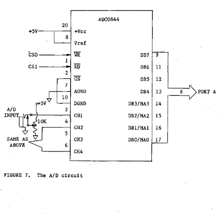
Port A was configured as an input port to accept the output lines
(DBO-DB7) of the N.S.C. ADC0844 A/D converter. The. A/D circuit is shown
in· Figure 7. A single circuit phone jack is provided for each A/D input
channel. A variable potentiometer is also provided to set any desired
voltage from 0 to 5
v.
When a phone plug is inserted into the jack, thepotentiometer ii? deactivated and the signal is coming via the phone plug.
[image:23.572.58.502.316.757.2]The ADC0844 is an 8-bit A/D converter with an analog input.multi-plexer (MUX). The 4 channel MUX can be programmed for 3 modes operat:Lon: single-ended, differential, or pseudo-differential. See Table 4.
TABLE 4. ADC MUX addressing
---~---MUX ADDRESS
MAJ MA2 MAl MAO
cs
WR---
xa L L L Lau
x L L H L
x L H L L
x L H H L
---
L H L L Lu
L H L H L
L H H L L
L H H H L
RD Ha H H H H H H H
Channel II
CHl CH2 CH3 CH4 AGND
+ + + + + + + + MUX MODE DIFFERENTIAL SINGLE-ENDED
---
H H L L L---
---u
HH H L H L H
H H H L L H
+
+
PSEUDO-D IFFERENT IAL
+
---
x x x x Lu
L--- ---
PREVIOUS CHANNEL CONFIGURATION---
---a H =High voltage ; L =Low voltage ; X =Don't care.
In this project, only the single-ended mode was used. Since the MUX address latches (MAO-MA3) are common with data bus lines (DBO-DB3), four steps.were needed for channel· selection:
[image:24.571.70.514.124.434.2]As perviously mentioned, port A and the control register of the 8255A PPI are located at memory locations %B800 and %B803, respectively.
An example which uses BASIC instructions to select channel 1 and to ac-·
cept the input signal from channel 1 is shown below. @%B803=%88
@%B802=0 @%B800=4 @%B802=15 @%B803=%98 @%B802=1 Y=@%B800 @%B802=15
Set port A to be an output port ADC0844 WR low
Send the proper value to port A to choose channel # 1 ADC0844 WR high; start conversion
Set port A to be an input port ADC0844 RD low
Accept input signal from port A ADC0844 RD high
The conversion time of the ADC0844 is 40 microseconds. If only BASIC instructions are used to do data processing, there will be no problem. If machine-language ins true tions are used, the time interval for acquiring the data should be longer than 40 microseconds. Otherwise, the ADC0844 will not have enough time to convert the data.
Port B was configured as an output port to connect to the input lines of an 8-bit buffer (74LS244), The buffer output lines were con-nected to the input lines of two 8-bit D/A converters (AD558) ti:> form two D/A outputs. Figure 8 shows the D/A circuitry.
The following BASIC commands select D/A #1 and D/A #2 and set their output voltages.
[image:25.568.48.520.49.595.2]2
4
6 PORT B>8 11 13 15 17 +sv 20 +Vee !Al 1A2 1A3 1A4 2Al 2A2 2A3 2A4 GND
10 l
AD558
8 DB7 Vout
7 DB6 vout SEN. 6 DBS vout SEL.
vs
DB4 GND4 DB3 GND
74LS244 3 DB2 CE
lG
19
~
L--2y4· 3 2 DBl +Vee
2Y3 5 l DBO
cs
2Y2 7 2Yl 9_
-1Y4 12
-1Y3 14 AD558
1Y2 16
-=-v
8~
SAME ASlYl ~
2G"
6
'
7TO SOLID-STATE RELAYS
&
ELECTROMECHANICAL RELAYSABOVE
cs
FIGURE 8. The D/A circuit
[image:26.572.69.503.62.640.2]@%B801=0 @%B801=255 @%B802=3 @%B801=128
D/ A Ill outputs zero vol ts D/A Ill outputs 2.56 volts Choose D/ A 112
D/A,112 outputs 1.28 volts
Not only the D/A outputs but also the relays were connected to port B. The 8-bit buffer provides the current to drive the D/A outputs and the relays.
The AD558 is a' voltage-output 8-bit D/A couverter. It will operate with any power supply voltage between +4.5 and +16.S
v.
There are two output ranges (0 to +2.56 V and 0 to +10 V). The 0 to +10 V output range requires a power supply of +11.4 to +16.5v.
In this system, the 0 to +2. 56 V output range was chosen since the system's power supply voltage was +5 V ,'Solid-state relays ( SSRs)
The output lines (1Yl-1Y4) of the 74LS244 buffer were wired to a bistable latch (74LS75). The latch's four output lines were wired to an inverting current buffer (SN75492), and the current buffer's output lines
[image:27.568.92.502.56.168.2]5V 5V 5V
5 11
+Vee +Vee
FROM
74LS244 74LS75 SN75492
2 16 14 1
lYl Dl Ql IN! OUT! THE BASICON
3 15 3 2
1Y2 02 Q2 IN2 OUT2 SERIES 6 FOUR
6 10 5 6
1Y3 03 Q3 IN3 OUT3 MODULE 110
v
7 9 8 7
1Y4 04 Q4 IN4 OUT4 MOUNTING SOCKETS
Gl G2 GND GND SYSTEM
4 13 12 4
1 2 110
VAC CS4
IA lY 74LS04
FIGURE 9. The SSR circuit
The following BASIC commands select the SSR circuit and operate the relays.
@%B802=4 Choose SSR circuit
[image:28.570.79.506.95.497.2]@%B801=15 Let all SSRs on
To turn any or all SSRs off, the command is @%B801=0. The latch is used for temporary storage of binary information. If the D/As and SSRs are used alternately, the latch will hold the SSR commands while the MC-lZ handles the D/A outputs. The D/A converter has its own built-in latch .and thus the two processes will not interfere with each other. The SN75492 current buffe·r supplies the necessary current to drive the SSRs.
The SSRs are useful for controlling high-current loads and for iso-lation. For example, if a short circuit happens in a light bulb circuit con trolled by the SSR there will be no damage to the MC-lZ.
Electromechanical relays (EMRs)
Two of the output lines (2Yl-2Y2) from the 74LS244 buffer were nected to another latch (74LS75). The latch's two output lines were con-nected to the two remaining input lines of the SN75492 current buffer. The current buffer's two remaining output lines were then connected to
the two EMRs. Figure 10 shows the EMR circuit.
The following BASIC commands select the EMR circuit and activate the relays.
@%B802=5 @%B801=16 @%B801=32 @%B801=48
Choose EMR circuit
Let EMR Ill on, the other off Let EMR 112 on, the other off Let all EMRs on
2A 2Y 74LS04
FIGURE 10. The EMR circuit
The sense switches
Four single-pole double-throw (SPDT) toggle switches were connected to a quad inverse SR latch (74LS279). The latch's output lines were con-nected through another buffer (74LS244) to the high nibble of port C. Figure 11 shows the sense switch circuit.
The following BASIC commands select the sense switch circuit and determine which switches are on or off.
@%B802=6
X=AND(@%B802, 240)/16
Choose the sense switch circuit
[image:30.571.49.497.51.480.2]sv
+sv
560K 560K 16FIGURE 11. The sense switch circuit
If X=l, switch #1 is on and others are off; if X=3, switches #1 and 2 are
on and the others are off.
[image:31.571.69.475.91.519.2]circui.t. Thus a buffer was used as a means to separate the signals coming from the sense switches and the keypad.
The keypad
The keypad (16 keys, 4X4 matrix) has 8 output lines, 4 for the rows and 4 for the columns. The keypad's output lines were connected to a 16-key encoder (MM74C922) and the encoder's output lines were connected to the high nibble of port
c.
Figure 12 shows the keypad circuit.The following BASIC commands select the keypad circuit and determine which pushbutton is pressed.
@%B802=7 Choose the keypad circuit
Y=AND(@%B801, 240)/16 Determine which. pushbutton is pressed
If Y=O, the /fl pushbutton is pressed; if Y=2, the 112 pushbutton is
pressed; if Y=l4, the E pushbutton is pressed; and if Y=lS, the D push-button is pressed.
1+SV
18
+Vee
MM74C922
11 17
Xl A PC4
10 16
X2 B PCS
8 15
X3
c
.
PC6I 7 14
1 2 3 4 X4 D PC7
COLUMNS
5 1 9
R Yl GND
~
6 2
4X4 0 Y2
7 3 6 Q.l uF
KEYPAD
w
Y3 KBM I8 4 I
s
Y4~
"OE
osc
13 5
CS7 -~ o.OluF
1
[image:33.575.59.451.59.674.2]System device control
The low nibble of port C was configured as output lines and were ·connected to a 4-line-to-16-line decoder (MM74Cl54). Only 8 (0-7) of the
16 output lines of the decoder were used as the control signals for the ·system. The remaining lines are for later expansion. The control lines
were assigned as O to CSO, 1 to CSl, ••• , etc. Figure 13 shows the cir-cuit for the control lines.
CSO and CSl which were connected to the ADC0844 A/D chip; ·cs2 and CS3 were connected to the AD558 D/A chips; CS4 was connected through an inverter (74LS04) to latch the SSR circuit; CSS was connected through the above mentioned inverter to latch the EMR circuit; CS6 was connected to the buffer of the sense switch circuit; and CS7 was connected to the keypad encoder. The following BASIC commands enable CSO, CSl, cs2, CS3, CS4, css, CS6, and CS7.
@%8802=0 Enable cso (edge triggered) @%8802=1 Enable CSl (edge triggered) @%8802=2 En.able CS2 (level triggered) @%8802=3 Enable CS3 (level triggered) @%8802=4 Enable CS4 (level triggered) @%8802=5 Enable css (level triggered) @%8802=6 Enable CS6 (level triggered) @%8802=7 Enable CS7 (level triggered)
Only one "CS0 signal can be enabled at a time. All others are disabled
PORT PCO PCl PC2 PC3
c
\7
23 22 21 20 12 18 19 ~5V 24 +Vee A Bc
D GND Gl G2 0 MM74Cl54 1 2 3 4 5 6 7 8 9 10 11 12 13 14 15FIGURE 13. The system device control l 2 3 4 5 6 7 8 9 10 11 13 14 15 16 17
cso
(A/D WR) CSl (A/D RD) CS2 (D/ A, Ill) CS3 (D/ A, 112) CS4 (SSRs) CS5 (EMRs) CS6 (S. S.) CS7 (KEYPAD) [image:35.575.61.480.107.612.2]SOFTWARE DEMONSTRATION OF CAPABILITIES
After the hardware is constructed, software is used for a
demonstra-tion which can let the user easily understand the whole system. Two
Zi-log books that will be invaluable to the user are "Z8671 single-chip
BASIC interpreter: BASIC/DEBUG software reference manual" and "ZS
microcomputer: Technical manual".
The following program will demonstrate the system's capabilities.
Program description follows the listing.
1 REM ---
ZB
DEMO (4-9-86) 10 A=%B800:B=A+l:C=A+2:D=A+320 @D=%98
30 @B=O:@C=2:@C=3:@C=4:@C=5
40 PRINT:PRINT
50 "WHAT DO YOU WANT TO DO?"
60 "1 )---A/D"
70 "2)---D/ A"
80 "3)---SENSE SWITCHES"
90 "4)---KEYPAD"
100 "5)---ELECTROMECHANICAL RELAYS"
110 "6)---SOLID-STATE RELAYS"
120 "7)---END THIS PROGRAM"
130 "PRESS 1-7 FOR CHOICE"
140 INPUT H
160 IF H>7 "TRY AGAIN,":GOTO 130 170 IF H=l GOSUB 300
180 IF H=2 GOSUB 400 190 IF H=3 GOSUB 500 200 IF H=4 GOSUB 600 210 IF H=5 GOSUB 700 220 IF H=6 GO SUB 800 230 IF H=7 STOP 240 GOTO 40
300 REM --- A/D SUBROUTINE
305 "PRESS 1-4 TO SELECT CHANNEL 1-4 AS INPUT CHANNEL."
310 "IF THE INPUT SIGNAL EQUALS ZERO, THIS SUBROUTINE IS EXITED." 315 INPUT X
320 IF X<=O "TRY AGAIN,":GOTO 315 330 IF X)4 "TRY AGAIN,":GOTO 315 340 @D=%88:@C=%F
350 @C=O:@A=X+3:@C=%F
360 @D=%98:@C=l:Y=@A:@C=%F:PRINT Y 370 IF Y=O GOTO 390
380 GOTO 340 390 RETURN
400 REM --- D/A SUBROUTINE
415 INPUT G
420 IF G<=O "TRY AGAIN,":GOTO 415 430 IF G)3 "TRY AGAIN,":GOTO 415 44.0 IF G=3 GOTO 480
445 @C=G+l 450 S=O
455 @B=S:S=S+l
460 IF S<255 GOTO 455 465 @B=S:S=S-1
470 IF S)O GOTO 465 475 GOTO 405
480 RETURN
500 REM --- SENSE SWITCH SUBROUTINE
510 "IF ALL SENSE SWITCHES ARE UP, THIS SUBROUTINE. IS EXITED." 520 @C=6
530 M=AND(@C,240)/16:PRINT M 540 IF M=l5 GOTO 560
550 GOTO 530 560 RETURN
600 REM --- KEYPAD SUBROUTINE
610 "PRESS THE D PUSHBUTTON OF THE KEYPAD TO LEAVE THIS SUBROUTINE." 620 @C=7
650 GOT0.630 660 RETURN
700 REM --- ELECTROMECHANICAL RELAYS SUBROUTINE
705 "PRESS 1 TO ACTIVATE RELAY 1; PRESS 2 TO ACTIVATE RELAY 2." 710 "PRESS 3 TO LEAVE THIS SUBROUTINE."
715 @C=5 720 INPUT K
730 IF K<=O "TRY AGAIN." :GOTO 720 740 IF. K)3 "TRY AGAIN." :GOTO 720 745 IF K=3 GOTO 795
750 IF K=2 GOTO 775 755 @B=O
760 @B=16:GOSUB 900 765 @B=O
770 GOTO 705 775 @B=O
780 @B=32:GOSUB 900 785 @B=O
790 GOTO 705 795 RETURN
800 REM --- SOLID-STATE RELAYS SUBROUTINE
805 "PRESS l TO ACTIVATE ALL RELAYS; PRESS 2 TO ACTIVATE RELAYS SEQUENTIALLY."
815 @C=4 .820 INPUT Z
830 IF Z(=O "TRY AGAIN.":GOTO 820 840 IF Z>3 "TRY AGAIN.":GOTO 820
845 IF Z=3 GOTO 895 850 IF Z=2 GOTO 870 855 @B=O:@B=l5:GOSUB 900 860 @B=O
865 GOTO 805
870 @B=O:@B=l:GOSUB 900 875 @B=2:GOSUB 900 880 @B=4:GOSUB 900 885 @B=8:GOSUB 900 890 @B=O:GOTO 805 895 RETURN
900 REM --- DELAY SUBROUTINE
910 V=O 920 V=V+l
930 IF V(25 GOTO 920 940 RETURN
1. Initialization (lines 1 to 30): Set port A & port C high nibble
to be input lines and port B & port C low nibble to be output lines; set A/D outputs at zero volts and deactivate all the re-lays.
2. User instructions (lines 40 to 130).
3. Error check and subroutine selection (lines 140 to 240) : Deter-mine whether the input value from the keyboard is correct or not and where to jump.
Lines 300 to 390 compose the A/D subroutine which does the following:
1. User instructions (lines 305 to 310): Use as a directory for what the A/D subroutine is doing.
2. Error check and channel selection (lines 315 to 330): Determine whether the input value from the keyboard is correct or not, de-cide which input channel is to be chosen.
3. Main body of subroutine (lines 340 to 390): Print the digital value of the input signal on the CRT screen.
Lines 400 to 480 make up the D/A subroutine which does the following:
1. User instructions (lines 400 to 410): Explain what this sub-rouUne is doing.
3. Main body of subroutine (lines 445 to 480): Produce a
triangular wave signal.
The subroutine for interpreting the sense switch settings resides. st - _ lines 500 to 560. If the switch is on, a high signal is sent to the
cor-responding line of port C high nibble. Otherwise, a low signal is sent to the same line. Upon receiving a signal from port C high nibble, the
subrou.tine prints a digital value on the CRT screen. If all the switches are off, the program leaves this subroutine.
Lines 600 to 660 compose the subroutine for reading the keypad. It
does approximately the same thing as the sense switch .subroutine. The only difference between the two subroutines is the source o.f the signal.
In one, the signal comes from the sense switches and in the other, it comes from the keypad.
The subroutine for controlling the electromechanical relays consists of lines 700 to 795. It does the following:
1. User instructions (lines 705 to 710): Explain what this sub-routine is doing.
2. Error check and relay selection (lines 715 to 750): Decide
whether the input value from the keyboard is correct or not and choose the exact relay to turn on or off.
3. Execution (lines 755 to 795): Activate/deactivate relay 1 or relay 2.
40
1. User instructions (lines 805 to 810): Explain what this
sub-routine is doing.
2. Error check and relay selection (lines 815 to 850): · Check whether the input value from the keyboard is correct or not and make program selection.
3. Execution (lines 855 to ·895): Activate/deactivate all relays simultaneously or sequentially.
A three-second .delay subroutine resides at lines 900 to 940. It is
needed because the program activates and deactivates the relays in a short amount of time. If there is no delay subroutine in this program the user is not sure that, the relays have been activated.
A Program to Count Heart Rate
One way to count the heart rate of a human subject correctly is by use of the electrocardiogram (ECG). The pattern of electrical .activity associated with the contraction of cardiac muscle during a heartbeat can be recorded by the procedure of alectrocardiography. This procedure pro-duces a recording called an ECG.
[image:43.571.64.509.66.346.2]ventricles need more strength to pump the blood, That is the reason why the amplitude of the QRS complex is much higher than that of the P wave. The QRS complex is a good target for use in counting the heart rate, If
the number of the QRS complexes during a period of time are counted, a determination of the heart rate in beats/minute can be made.
VOLTAGE
R
T
p
Q
s
---TIME
FIGURE 14. A normal ECG waveform
An ECG simulator was used to produce an appropriate signal and a
[image:44.568.67.404.230.530.2]the MC-lZ MCU was used as a timer, This required connecting line P3(6) to line P3(1), Because the. duration of the QRS complex of the ECG signal is approximately 0.08 seconds (Milnor, 1974), a program using only BASIC instructions would be too slow to detect the QRS complex. Thus a machine language subroutine was wri·tten to detect the QRS complex and BASIC in-structions handled the remaining parts of the program. The following program displays the heart rate of a human subject on the CRT.
10 A=%B800:B=A+l:C=A+2:D=A+3 20 @D=%98
30 @B=O:@C=2:@C=3:@C=4:@C=5 40 @38=130:@39=30
50 @247=%41:@243=0:@242=0:@241=%46 60 G0@%3900
70 PRINT:PRINT
80 IF @242=0 "HEART RATE= 0 BEAT/MINUTE":GOTO 110 90 H=256-@242:Z=l50*60/H
100 PRINT "HEART RATE=";Z;"BEATS/MINUTE"
110 "PRESS l TO CONTINUE; PRESS ANY OTHER KEY TO STOP" 120 INPUT X
130 IF X=l GOTO 20 140 STOP
LOC. OP. CODE
%3900 SRP %30
HEX. CODE
%3902 LD rO, 0
oc
00%3904 LD rl, 1 lC 01
%3906 LD r2, %F 2C OF
%390B LD r3, %BB 3C BB
%390A LD r4, %9B 4C 9B
%'390C LD rs, 4 SC 04
%390E LD r6, %BB 6C BB
%3910 LD r7, 3 7C 03
%3912 LD rB, %BB BC BB
%3914 LD r9, 2 9C 02
%3916 LD rA, %BB AC BB
%391B LD rB, 0 AC 00
%391A LD R40, %FF E6 2B FF
%3910 LD R41, %FF E6 29 FF
%3920 LD R34, 4 E6 22 04
%3923 DEC R34 00 22
%392S JP NZ,%3923 ED 39 23
%392B DECW R,40,41 BO 2B
%392A JP Z,%39BB 6D 39 BB
%392D LDE @rr6,r3 92 36
%392F LDE @rrB,r2 92 2B
%3931 LDE @rrB,rO 92 OB
%3933 LDE @rrA,rS 92 SA
%393S LDE @rrB,r2 92 2B
%3937 LDE @rr6,r4 92 46
%393B LDE @rC,@rrA 82 CA
%393D LDE @rr8,r2 92 28
%393F CP R38,R60 A4 26 3C
%3942 JP ULT,%3920· 7D 39 20
%394S LD R241, %4A E6 Fl 4A
%3948 LD R3S, 4 E6 23 04
%394B DEC R3S 00 23
%394D JP NZ,%394B ED 39 4B
%39SO LDE @rr6,r3 92 36
%39S2 LDE @rr8,r2 92 28
%39S4 LDE @rr8,r0 92 08
%39S6 LDE @rrA,rS 92 SA
%39S8 LDE @rr8,r2 92 28
%39SA LDE @rr6,r4 92 46
%39SC LDE @rr8,rl 92 18
%39SE LDE rD,@rrA 82 DA
%3960 LDE @rr8,r2 92 28
%3962 CP R39,R61 A4 27 3D
%396S JP UGT,%3948 BD 39 48
%3968 LD R36, 4 E6 24 04
%396B DEC R36 00 24
%396D JP NZ,396B ED 39 6B
%3970 LDE @rr6,r3 92 36
%3972 LDE @rr8,r2 92 28
%3974 LDE @rr8,r0 92 08
%3978 LDE @rr8,r2 92 28
%397A LDE @rr6,r4 92 46
%397C LDE @rr8,rl 92 18
%397E LDE rE,@rrA 82 EA
%3980 LDE @rr8,r2 92 28
%3982 CP R38,R60 A4 26 3E
%3985 JP ULT,%3968 7D 39 68
%3988 LD R241, %42 E6 Fl 42
%398B RET AF
The BASIC program resides in lines 10 to 140. It does the
follow-ing. 1.
2.
Lines 10 to 30 set port A and port C high nibble to be input lines and port B and port C low nibble to be output lines. This part also sets the A/D outputs at zero volts and deactivates all the relays.
Line 4.0 sets the high- and low-voltage levels for de tec·ting the
QRS complex of the ECG signal. If the high-voltage level is' ~et
too high or too low, the program will not detect the QRS complex or the P wave and the T wave will be erroneously detected,
respectively. The high-voltage level should be set below the height of QRS complex but above those of the P wave and the T wave. If only one voltage level for de tee ting the QRS complex
3. Line 50 causes a 9600 Hz signal from timer 0 to be divided by 64 to produce a 150 Hz signal. It also loads C/T 1 with the value of 256 and holds C/T l off.
4. Lines 80 to 100 acquire a value from C/T 1, mske a calculation (which will be described later), and print the heart rate on the CRT screen. Because the value from C/T l is 256 or less (assume. the value is X), the actual value would be (256-X). The actual value is produced by a 150 HZ signal, so the real time interval
is (256-X)/150. The detecting procedure counts the time
inter-val of two consecutive QRS complexes. The true heart rate thus is 150*60/(256-X).
5. Lines 110 to 140 print instructions to the user to allow a repeat heart rate determination or program termination. Memory locations %3900 to %398B hold the machine language sub-routine. The subroutine does .the following.
1. Locations %3900 to %3919 store the numbers that the subroutine
uses for port setting and channel selection.
2. Locations %391A to %3944 check for a no-signal conqition for 10 seconds. If no signal is de tee ted the subroutine is exited, otherwise it continues.
3. Locations %3945 to %3967 turn C/T l on and then Wait for the am-plitude of the QRS complex to drop below the low-voltage level. 4. Locations %3968 to %398B check for another QRS complex to appear
with its amplitude above the high-voltage level. If so, C/T l
CONCLUSION
This single-board-computer data acquisition system has four A/D input channels, two D/A output channels, four SSRs, two EMRs, four sense switches, and a keypad. The A/D can be programmed as four single-ended channels or three pseudo-differential channels or two differential chan-nels. The D/A output channel can supply 0-2.56
v.
It should not be us.ed as a control power supply.. The four SSRs and two EMR.s can be used to control other devices. The four sense switches and a keypad can b.e used as inputs to control the system.This system uses the BASIC language for its programming. It can also be programmed in machine-language to increase execution speed. The system needs a power supply of +5 V to operate. Because a back-up bat-tery is included, if the system is shut off, the RAM-stored data will be maintained. If a programming module (and its utility PROM) are used, you can copy an application program from RAM to EPROM. You can also copy the EPROM back to RAM for debugging purposes.
The techniques in building a computer system will improve with time. The size of the computer will decrease and its performance and numbers of functions will increase. The
·zs
data acquisition system is compact and portable.. Its capabilities are approximately the same as an older·PDP-8-based data acquisition system in use in the Biomedical Engineering Program at Iowa State University.
single-board compu.ters are having on instrumentation development. The flexibility that can result from using a single-board computer is
undeni-able. It is easy to adapt a single-board computer-based instrument to a new circumstance by simply changing an EPROM. The potential also exists for reducing the time from project inception to project completion as a
BIBLIOGRAPHY
Basicon, Inc. 1984. MC-lZ Microcontroller. Basicon, Inc., 11895 N.W. Cornell Road, Portland, OR.
Bolton, M. P.; Taylor A. C. system for the disabled 3(4): 281-284.
1981. A universal computer and interface (unicaid). J. Biomedical Engineering
Brown, A. W. S. 1981.
monitoring system. A microprocessor-based ultrasonic limb movement J. Biomedical Engineering 3(4):275-279. Demjaneko,
V.;
Sachs, F. 1982. Computer interface for electrophysiologyapplications: Simple modifications to a commercial (Datel) single-board data-acquisition system. J. Medical
&
Biological Engineering&
Computing 20(1):65-69.Dostinsky, I. A.; Christov, C. L.; Daskalov, I. K.
microprocessor-electrocardiograph. J. Medical Engineering & Computing 23(3):209-211.
1985. A
&
BiologicalEl-Dhaher, A. H. G.; Kaouri, H. A.; Mustafa, K. Y. 1983.
Microprocessor-based system for the measurement and analysis of an expiratory flow-volume curve. J. Medical & Biological Engineering
&
Computing 21(3):277-284.
Imperials, Cosimo. 1983. Microprogrammed data acquisition system for renography. J. Clinical Engineering 8(3):235-241.
Milnor, William R. 1974. The electrocardiogram. Pages 883-891 in
Vernon B. Mountcastle, ed. Medical physiology. 13th ed. The C.
v.
Mosby Company Press, Baltimore, Maryland.Plexico, Perry S. 1980. Microcomputer applications in biomedical researc.h. J. Medical Instrumentation 14(6):307-310.
Ramey, R. L.-; Johnson, B. W.; Aylor, J. H. 1982. Microcomputer-based aid for the handicapped computer programmer. J. Medical
&
Biological Engineering
&
Computing 20(6):640-644.Rolander, Clas I. 1984. Communication aids for the vocally handicapped using voice synthesis technology, an LCD text display and a
single-chip microcomputer. M.S. thesis. Iowa State University, Ames.
Wuthnow, Mark; Manoli, Samir; Schroder, Darrell. Microcomputer-based arrhythmia monitor. J.
9(4) :291-29S.
19S4.
Clinical Engineering
Zilog, Inc. 19SO. Z.S PLZ/ ASM: Assembly language programming manual. Zilog publication ref. no.: 03-3023-02. Zilog Inc., 1315 Dell Ave., Campbell, CA.
Zilog, Inc. 19Sl. ZS671 single-chip BASIC interpreter: BASIC/DEBUG software reference manual. Zilog publication ref. no.: 03-3149-02. Zilog, Inc., 1315 Dell Ave., Campbell, CA.
Zilog, Inc. 19S3. ZS single-chip microcomputers technical overview. Zilog Inc., 1315 Dell Ave., Campbell, CA.
ACKNOWLEDGEMENTS
I would like to acknowledge the enthusiastic suppor-t offered by my major professor, Dr. Curran S. Swift, and I would like to thank him for his openness and willingness to help. I would also like to thsnk
Dr. Richard E. Horton and Dr. David L. Carlson for serving as members of my comm! t tee.
In addition, I would like to extend my thanks to Mike A. Anderson and Dexter K. Ishii for the many learning experiences we shared together. I would also like to acknowledge the very important and constant en-couragement that has been provided by my parents and wife.
APPENDIX: MANUFACTURERS OF SINGLE-BOARD 'BASIC' COMPUTERS
1. Antona Corporation. 2100 S Sawtelle Blvd., Suite 205, West Los Angeles, CA 90025 (213) 473-8995
2. Basicon, Inc, 11895 NW Cornell Road, Portland, OR 97229 (503) 626-1012 (I, N2,
z
3)3. Digi-Key Corporation. 701 Brooks Avenue South, P.O. Box 677, Thief River Falls, MN 56701 (218) 681-6674 (N)
4. Global Automation. 2829 Lewis Lane, Owensboro, KY 42301 (502) 683-9871 (I)
5. H. H. S. Microcontrollers. 5876 Old State Road, Edinboro, PA 16412 (814) 734-4338 (Z)
6. Lehmann
&
Associates. P.O. Box 566, Maumee, OH 43537 (419) 891-0687 (Z)7. Messand Microprocessor Engineering. 1509 Francis Street, Al-bany, CA 94706 (415) 526-5155 (Z)
8. Micro Linear Controls. 4900 Memco Lane, Racine, WI 53404 (414) 639-1105 (I)
9. Micromint, Inc. 561 Willow Avenue, Cedarhurst, NY 11516 (516) 374-6973 (I, Z)
l I = Intel 8052AH-BASIC product.
2 N
= National Semiconductor INS8073 product,
10. Octagon Systems Corporation. 6501 W 91st Avenue, Westminster,
co
80030 (303) 426-8540 (N)11. Schulz Enterprises Inc. 1285 Las Tunas Drive, San Gabriel, CA 91776 (818) 287-5067 (Z)
12. Tech Star Laboratory. Suite 709, R&B Corporation Park, 1701 N. Greenville Avenue, Richardson, TX 75081 (I)