Compton Imaging for Homeland Security
Thesis submitted in accordance with the requirements of the University of Liverpool for the degree of Doctor in Philosophy
by
Anthony Sweeney
Abstract
This work marks the first use of a fully digital trigger system and new CAEN V1724
digitisers to create a Compton camera from two semiconductor double sided strip
de-tectors. The system was designed to be able to identify and locate gamma ray emitting
radionuclide within an energy range of 60 to 1408keV. Compton images were produced
at AWE Aldermaston and the University of Liverpool across an energy range of 80 to
1408keV, using point sources, extended sources and also including special nuclear
ma-terials. The image at 80keV is the lowest recorded energy for a Compton image using
a two detector cryogenically cooled Compton camera. GAMOS simulations have been
used to check the experimental data and provide evidence that indicates if pulse shape
analysis was applied to the experimental data the image resolution would be improved
Contents
Abstract i
Contents v
List of Tables xxi
List of Figures xxi
Acknowledgement xxii
1 Introduction 1
1.1 AWE . . . 2
1.2 Research work . . . 3
1.3 Current technologies . . . 3
1.3.1 RadScan 800 and CARTOGAM . . . 4
1.3.2 Use of Compton camera systems . . . 5
2 Principles of gamma ray detection 6 2.1 Gamma ray production . . . 6
2.2 Interaction of radiation with matter . . . 7
2.2.1 Photoelectric absorption . . . 7
2.2.2 Compton scattering . . . 8
2.2.3 Pair production . . . 9
2.2.4 Linear attenuation coefficient . . . 10
2.3 Interactions of charged particles with matter . . . 11
2.3.1 Collisional energy loss . . . 11
2.3.2 Radiative energy loss . . . 11
2.4 Solid state gamma-ray detectors . . . 12
2.4.1 Semiconductors . . . 12
2.4.2 Scintillation detectors . . . 21
2.4.3 Energy resolution . . . 23
2.5 Signal generation . . . 25
2.5.2 Preamplifier . . . 26
2.5.3 Parametric pulse shape analysis . . . 27
3 Compton camera principles 32 3.1 Mechanical collimation . . . 33
3.1.1 Pin hole collimated detectors . . . 33
3.1.2 Coded aperture . . . 34
3.2 Compton camera principles . . . 35
3.2.1 Detector setup . . . 35
3.2.2 Detector qualities for a Compton camera . . . 36
3.2.3 Errors in Compton cameras . . . 37
3.3 Image reconstruction . . . 38
3.3.1 Analytical back projection . . . 39
3.3.2 Iterative . . . 42
4 Detector and electronics overview 45 4.1 Detectors used . . . 45
4.1.1 Silicon lithium (SiLi) scatter detector . . . 45
4.1.2 DC01 and AC13 . . . 46
4.1.3 High purity germanium absorber detector . . . 47
4.2 Digital electronics . . . 47
4.2.1 High voltage (HV) and preamplifier power . . . 49
4.2.2 GO Box . . . 49
4.2.3 CAEN V1724 Digitiser . . . 50
4.2.4 CAEN V1495 Trigger logic controller . . . 52
4.2.5 CAEN V2718 Optical link bridge . . . 52
4.2.6 MIDAS . . . 52
4.3 Energy calibration . . . 52
5 Experimental results from Liverpool 54 5.1 Detector setup . . . 54
5.2 Energy Calibration . . . 55
5.3 Timing resolution . . . 56
5.4 Point source measurements . . . 59
5.4.1 Compton efficiency . . . 59
5.4.2 133Ba . . . 65
5.4.3 57Co . . . 68
5.5 Distance of source to detector investigation . . . 72
5.6 22Na line source . . . 75
5.7 Scan measurements . . . 77
5.7.1 137Cs scan . . . . 78
5.7.2 133Ba scan . . . 80
5.8 Multiple sources . . . 83
5.8.1 137Cs and 60Co . . . 85
5.8.2 137Cs and 133Ba . . . 87
5.9 Summary . . . 87
6 Experimental results from Aldermaston 96 6.1 Detector setup . . . 97
6.2 Measurements taken at Aldermaston . . . 97
6.2.1 Calibration . . . 97
6.2.2 Point source measurements . . . 99
6.2.3 Distributed sources . . . 108
6.3 Summary . . . 112
7 GAMOS Simulation 115 7.1 GAMOS . . . 116
7.2 Compton camera simulation . . . 116
7.3 Validation . . . 116
7.3.1 Efficiency . . . 117
7.4 Simulating the effect of smaller pixels . . . 121
7.4.1 Image charge analysis . . . 121
7.4.2 Application to the absorber . . . 121
7.5 Best slice simulation . . . 125
7.6 Summary . . . 126
8 Conclusion and discussion 127 8.0.1 Comparison of Aldermaston and Liverpool results . . . 128
8.0.2 Energy range . . . 130
8.0.3 Efficiency . . . 131
8.0.4 Image reconstruction . . . 132
8.0.5 Discussion . . . 133
A Experimental images taken in Liverpool 135 A.1 152Eu Images . . . 135
B Experimental images taken in Aldermaston 142 B.1 152Eu Images . . . 142
List of Tables
2.1 Properties of intrinsic silicon and germanium, from [15] . . . 14
5.1 This table shows the counts per second (cps) recorded for a single strip
on each detector through an analogue system compared to the digital
system. The analogue circuit should have no dead time, so this provides
an estimate of the dead time caused by the digital electronics. The
average values of each are compared as a percentage to give a 7.5% dead
time for the scatterer and a 9.9% dead time for the absorber. A value
of 10% will be used for the efficiency calculation to allow for the reading
out of 48 channels worth of data rather than just single channels. . . 60
5.2 This table shows the spectroscopic information gained from the 152Eu
Compton run taken at Liverpool used for an absolute efficiency
calcula-tion. There is a 10% error on the energy resolution measurements. . . . 62
5.3 Position and FWHM of the image from 152Eu taken at Liverpool for 3mm compression, except for the 122keV image which was taken using
5mm compression. . . 64
5.4 Average FWHM and angular resolution of the images from152Eu taken at Liverpool for 3mm compression for all peaks except 122keV which has
a 5mm compression. . . 64
5.5 Position and FWHM of the image from133Ba taken at Liverpool. . . 68 5.6 Position and FWHM of the image from 133Ba taken at Liverpool, at
80keV with an angle gate of 0 to 130 degrees. . . 71
5.7 The effect on the amount of data imaged when an angle gate is applied.
The percentage data lost is included. . . 72
5.8 Position and FWHM of the image from57Co taken at Liverpool. . . 73 5.9 Gradients and intercepts from the fits to the best Z slice versus distance
from detector can. . . 73
5.10 Position and FWHM of the image from 22Na line source placed along the both axes. . . 77
5.11 This table shows the relative separation in X between the three different
5.12 This table shows the relative separation in Z between the three different
sources, two137Cs and one60Co as measured by the Compton camera. . 86
5.13 This table shows the relative separation in X between the three different
sources, two137Cs and one133Ba as measured by the Compton camera. 87 5.14 This table shows the relative separation in Z between the three different
sources, two137Cs and one133Ba as measured by the Compton camera. 87 5.15 Summary table showing the measured position of the source compared
to the expected position for the Liverpool data. The expected positions
have an error of±5mm. . . 88
5.16 Summary table showing the average FWHM and angular resolution for
the Liverpool data. . . 89
6.1 This table shows the details of all the data runs collected at Aldermaston
with the detector in Compton mode. . . 99
6.2 Position and FWHM of the image from 57Co taken at Aldermaston for 3mm compression. . . 100
6.3 This table shows the spectroscopic information gained from the 152Eu addback spectrum taken at Aldermaston. . . 103
6.4 Position and FWHM of the image from152Eu taken at Aldermaston. . . 105 6.5 Average FWHM and angular resolution of the images from152Eu taken
at Aldermaston for 3mm compression. . . 105
6.6 Position and FWHM of the image from152Eu taken at Aldermaston for 1mm compression. The 122, 244, 344, 443 and 778keV photopeaks were
combined to get this result. . . 106
6.7 Position and FWHM of the image from133Ba taken at Aldermaston. . . 108 6.8 Position and FWHM of the image from 235U taken at Aldermaston for
3mm compression. . . 109
6.9 Position and FWHM of the image from239Pu taken at Aldermaston for 3mm compression. . . 111
6.10 Summary table showing the measured position of the source compared
to the expected position. The expected positions have an error of±30mm.113
6.11 Summary table showing the average FWHM and angular resolution for
the Aldermaston data. . . 114
7.1 Simulated and experimental FWHM measurements for comparison. . . . 117
7.2 Simulated effects of using different voxel sizes in the absorber while
keep-ing the scatterer voxels at 5x5mm. . . 123
7.3 Simulated effects of using different voxel sizes for the scatterer, while
7.4 Simulated effects of using different voxel sizes on the scatterer and
ab-sorber at the same time, using the same voxel size in each detector. . . . 125
7.5 The percentage number of counts available to image when different sized voxels are used for both detectors at the same time. . . 125
8.1 Comparison of the angular image resolution measured using peaks from 152Eu and133Ba at Aldermaston and Liverpool . . . 130
C.1 Branching ratios of the gamma ray energies emitted by 57Co. . . 149
C.2 Branching ratios of the gamma ray energies emitted by 133Ba. . . 149
C.3 Branching ratios of the gamma ray energies emitted by 152Eu. . . 150
C.4 Branching ratios of the gamma ray energies emitted by 22Na. . . 150
C.5 Branching ratios of the gamma ray energies emitted by 235U. . . 150
List of Figures
2.1 Relative importance of the three major interactions of gamma rays with
matter. The lines indicate values ofZandEγfor which the neighbouring
effects are just equal. Diagram reproduced from [13].T is the probability of a photoelectric effect,σis the probability of a Compton scatter andκis the probability of a pair production. The green and red lines indicate the
detector materials used in this project, germanium and silicon respectively. 7
2.2 Illustration of the main gamma-ray interaction mechanisims that occur
with matter. (a) shows photoelectric absorption, (b) is Compton
scat-tering and (c) is pair production. Red lines indicate particle movement,
green lines areγ rays. . . 8 2.3 The Klein Nishina distribution shows that for higher energy gamma rays
it is more probable that they will Compton scatter in a forward
direc-tion. For energies around 10MeV the gamma rays are preferentially
scattered in a forward direction where as for energies less than 100keV
the distribution becomes more symmetrical about the 90 degree axis. . . 10
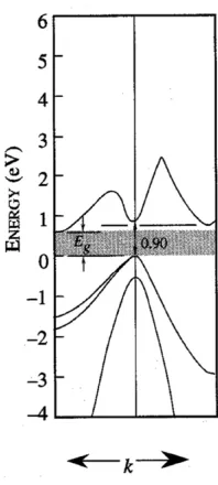
2.4 Band structure of germanium, shown in terms of the electron energy, E
and the effective electron momentum,k. The shaded region corresponds to the band gap, the region of forbidden energies. The valence band and
conduction band are therefore the bands below and above the shaded
area respectively. . . 13
2.5 Illustration of the electron energy bands allowed within semiconductors
and insulators. The band gap is a forbidden region in which no electrons
can remain, an insulator has a band gap of 5eV or more compared to
around 1eV for a semiconductor. . . 14
2.6 Doping with phosphorus creates an n-type semiconductor. A phosphorus
atom substitutes for a silicon atom within the crystal in this example,
creating a donor level due to its extra electron. This donor level exists
2.7 Doping with boron creates an p-type semiconductor. A boron atom
sub-stitutes for a silicon atom within the crystal in this example, creating an
acceptor level due to the non covalent bond formed with one
neighbour-ing silicon atom. This acceptor level exists within the band gap of the
material close to the valence band. . . 17
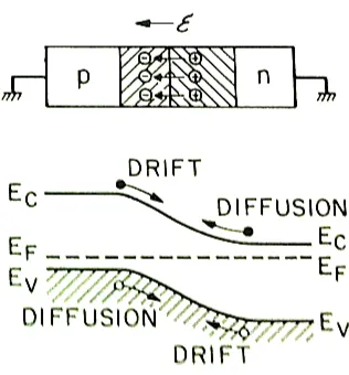
2.8 A depiction of a p-n junction, indicating the direction of electron
diffu-sion, from n-type to p-type and also the drift of the holes. The depletion
region formed is shown by the shaded area. Figure reproduced from [16]. 17
2.9 Current flow across a p-n junction when a bias voltage is applied. . . 19
2.10 A schematic of the diamond cubic crystal lattice, based on the face
cen-tered cubic (fcc) bravais lattice. This is the crystal formed by both silicon
and germanium. . . 20
2.11 A schematic showing the lattice planes of an fcc crystal structure<100>,
<110>and <111>marked (a),(b) and (c) respectively, in terms of the Miller indices. . . 20
2.12 Experimental electron drift velocities in germanium along the<111>and
<100>planes. The <110>direction is also shown, this has been simu-lated. Diagram reproduced from [18] . . . 21
2.13 A schematic diagram showing the function of a scintillator and PMT
when incident radiation interacts within the detector material. Electrons
are produced by the gamma ray interaction, the subsequent de-excitation
of these electrons produces light. The light photons are collected by the
photocathode, and the subsequently produced electrons are accelerated
through the PMT, being amplified as they pass through the dynodes to
produce an output signal on the anode. . . 22
2.14 Variation of the FWHM of a full energy peak within a germanium
detec-tor with incident gamma-ray energy. Each facdetec-tor discussed is represented
individually and the combination WT of these factors is shown. Figure
reproduced from [15] . . . 25
2.15 Schematic representation of the weighting field within a strip detector,
reproduced from [23]. The current pulses induced by the movement of
a charge carrier (q) are shown at the bottom of the diagram. As charge travels along line 1, it can be seen that the induced current decreases
with distance from electrode 1. As charge moves along line 2 the induced
current shape is bipolar due to the weighting field direction changing
along the path. . . 27
2.16 Circuit diagram of a typical charge sensitive preamplifier as used with
semiconductor detectors. . . 28
2.18 A typical pulse seen from a HPGe DSSD. T30 marks the point at which
the majority of primary charge carriers for the contact have been
col-lected, while T90 represents the time at which the majority of the
sec-ondary charge carriers have been collected. . . 29
2.19 Typical pulses seen from a silicon (a) and a germanium (b) detector with
the pulses seen in neighbouring strips included alongside. The image
charges are lost in the silicon detector due to being below the noise level,
however they are clearly visible in the germanium detector. . . 31
3.1 Schematic diagram of a pinhole collimator. The blue lines represent
gamma rays that are absorbed by the collimator, only the red gamma
ray will be enter the detector material. . . 33
3.2 Coded aperture mask, showing the shadows created by two different
sources A and B. Diagram reproduced from [32]. . . 34
3.3 A two detector Compton camera. Gamma-rays Compton scatter in the
scatterer and are subsequently absorbed via photoelectric absorption.
The back projected cone has an opening angle θ calculated from the Compton scattering equation (Equation 2.3). The cone axis is positioned
using the vector between the two interaction points. . . 35
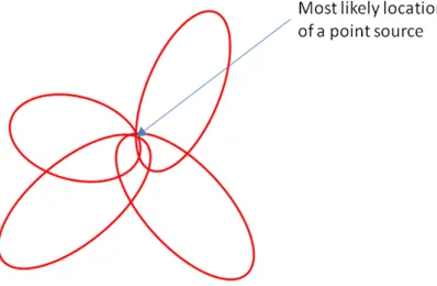
3.4 Multiple events will allow multiple cones to be generated. Taking a slice
perpendicular to the z axis, the area of most overlap of the conics in this
slice is the probable source location. . . 36
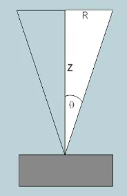
3.5 A simple case showing a gamma-ray Compton scattering from the front
edge of the scatterer. Knowing the scattering angle θ the half radiusR
of the cone can be calculated for a given distance Z using trigonometry. 39 3.6 Examples of images created with 10 (a), 100 (b) and 1000 (c) conics. As
the number of cones increases the source position is located more
accu-rately, with the source positioned at the point of most overlap. These
images are taken from the same GAMOS simulated data set. The black
box on the image indicates the position of the absorber detector in
rel-ative space. . . 39
3.7 Examples of the cuts taken through the X (a) and Y (b) axes taken from
the GAMOS simulated data set. The Lorentzian fit is shown for each
overlaid in green with the quadratic background in blue. This fit is used
to provide the location of the source from the mean value and also the
FWHM of the image, taken from the standard deviation of the fitted
curve. . . 40
3.8 Plot of the FWHM found in X against the Z slice. The source position
3.9 Schematic diagram showing the zero of Z for imaging purposes as being
the back edge of the absorber crystal. . . 41
3.10 Examples of different compression factors, 3 and 5 mm. The image and
cut through shown in (a) and (c) are using a 3mm compression, while
those in (b) and (d) are using a 5mm compression. From these examples
it is clear that although the statistics improve the FWHM of the image
increases as the compression increases. . . 43
4.1 Schematic diagram of the strip configuration of the SiLi detector used as
a scatterer (a) along with pictures of the detector unit itself (b) and (c).
Images (a) and (c) are reproduced from [38]. Image (b) was provided by
Canberra France. . . 46
4.2 Energy resolution measured for the SiLi detector. (a) shows the energy
resolution at 60keV for the AC side and DC side compared to
measure-ments taken by Canberra, with the source in different locations.(b) shows
the energy resolution at 662keV for both sides of the detector. . . 48
4.3 Schematic diagram of the strip configuration of the HPGe detector used
an absorber (a) along with a picture of the detector unit itself (b). Image
(a) reproduced from [41]. Image (b) reproduced from [42]. . . 49
4.4 Flow diagram of the digital electronics used for this work. The GO Box
provides an amplified signal from each detector output to the CAEN
V1724 digitiser cards. Energy thresholds are set on the V1724’s and
the signal from any channel which is above the appropriate threshold
is passed to the CAEN V1495 trigger control card. The trigger logic
programmed onto the V1495 is checked and if passed a signal is sent
back to the V1724’s to read out the appropriate data to the MIDAS
data acquisition software via an optical link using the V2718 and A2818. 50
4.5 Picture showing the gain/offset (GO) box used to provide additional
am-plification to the preamplifier signals and also provide a common baseline
level. . . 51
4.6 Picture showing the CAEN V1724 digitiser cards in a VME crate. 3 cards
are shown with the clock and optical readout cables in place, along with
the V2718 optical link bridge card which is at the left hand side of this
image. . . 51
4.7 Energy spectra demonstrating the calibration of two channels of the
HPGe detector. The calibration matches all of the channels to the same
bin to energy ratio. A quadratic fit is used across a wide energy range
using sources that provide known gamma ray energies, this example
5.1 Pictures of the Compton camera system mounted above the scanning
table at Liverpool. The scanning table was used to align the detectors to
within±1mm using the 1GBq137Cs collimated source contained within the table, this source was shielded with lead to prevent any interference
with measurements taken after the alignment. . . 55
5.2 Position histograms showing the scatterer (a) and absorber (b) generated
by scanning the Compton detector system with a 1Gbq 137Cs source mounted in a scanning table. The raster scan was carried out in 1mm
steps with the source in one position for 10 seconds. The centres of
each detector are aligned to within 1mm of each other in X and Y.
The scatterer is missing one strip from the AC (AC13) side and also
two strips from the DC (DC01 and DC02) side, this is due to double
peaking being seen from DC02 and DC01 and AC13 being removed for
previously stated reasons. The images here are fold 1 gated, so DC11 on
the absorber is missing due to its lack of fold one events. . . 56
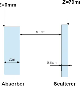
5.3 Schematic diagram showing the detector separation used for the
experi-ments at Liverpool. . . 57
5.4 Flow diagram of the electronics used to measure the time resolution
between the two detectors. The time to amplitude converter (TAC)
provides an output with a voltage proportional to the time difference
between signals received at its start and stop inputs. . . 58
5.5 Time coincidence peak seen in MAESTRO between the scatterer and
absorber detectors. The FWHM of this peak is measured as 150ns, with
a FWTM of 298ns. These values indicate that a coincidence trigger
window of 250ns should be adequate to encompass the majority of true
coincident events between the detectors. The measurement was carried
out at 511keV. . . 58
5.6 Addback energy spectra from a 152Eu source. This energy spectra was used to produce an absolute efficiency curve for the Compton camera. . 61
5.7 Absolute Compton efficiency for a152Eu source placed 11.6cm from the scatterer crystal. The error is estimated at 10% for each point allowing
for counting errors, timing errors and any errors in the source activity. . 61
5.8 Images created by applying an energy gate around the 122keV photopeak
of152Eu. The images have different angle gates applied, (a) 0 to 180, (b)
0 to 90 and (c) 0 to 70. The application of an angle gate on the Compton
scattering angle for each event removes the back scattered events present
5.9 The image produced by gating on the 122keVγ ray from152Eu with a 0 to 60 degree angle gate included is shown in (a) with a 5mm compression.
The average FWHM of the image is 21.7mm ± 2.9mm. (b) and (c)
are cross sections through the X and Y axis respectively, showing the
Lorentzian fit to the data used to create the image. . . 63
5.10 Average image resolution plotted against the gamma ray energy, the
number of cones used to create the images has been limited to the same
number providing a direct comparison. . . 65
5.11 The image produced by gating on the 1408keVγ ray transition is shown in (a). The average FWHM of the image is 16.7mm ±1.1mm. (b) and
(c) are cross sections through the X and Y axis respectively, showing the
Lorentzian fit to the data used to create the image. . . 66
5.12 The image produced by gating on 122, 244, 344, 443 and 778keV γ
rays from 152Eu is shown in (a) with a 3mm compression. The average FWHM of the image is 20.4mm±1.1mm. (b) and (c) are cross sections
through the X and Y axis respectively, showing the Lorentzian fit to the
data used to create the image. . . 67
5.13 Addback energy spectra from a 133Ba source. . . 68 5.14 The image produced by gating on 276, 302, 356 and 383keVγ rays from
133Ba is shown in (a) with a 1mm compression. The average FWHM of
the image is 21.8mm ± 0.4mm. (b) and (c) are cross sections through
the X and Y axis respectively, showing the Lorentzian fit to the data
used to create the image. . . 69
5.15 The image produced by gating on the 80keVγ ray from 133Ba is shown
in (a) with a 25mm compression. The average FWHM of the image is
135.0mm±21.4mm. (b) and (c) are cross sections through the X and Y
axis respectively, showing the Lorentzian fit to the data used to create
the image. . . 70
5.16 Addback energy spectra from a 57Co source. . . . 71
5.17 The image produced by gating on the 121keVγ ray from57Co is shown in (a) with a 3mm compression but no angle gate applied. To resolve the
source an angle gate of 0 to 60 degrees is applied, this image is shown
in (b) with a 3mm compression. The average FWHM of the image is
32.3mm ± 1.5mm. (c) and (d) are cross sections through the X and Y
axis respectively, showing the Lorentzian fit to the data used to create
5.18 Plot showing fits to the best slice found using the FWHM in X and in
Y as previously discussed in Chapter 4.(b) and (c) show two examples
of the FWHM in X plotted againt the Z slice imaged. The best slice is
taken at the minima of the curve. The actual position is marked in red,
where as the best image slice is marked in green. . . 74
5.19 Schematic diagram showing the positions in which the 22Na line source was positioned with relation to the detector crystals along the X and Z
axes. (a) shows the source placed perpendicular to the X axes, (b) shows
it parallel to X. . . 75
5.20 Pictures of the 22Na source, showing the length (50mm), width (4mm) and the placement in parallel and perpendicular to the detector cans. . 76
5.21 Addback energy spectra from a 22Na line source. . . 77 5.22 The image produced by gating on 511 and 1274keV is shown in (a) with a
5mm compression. The FWHM in X of the image is 42.0mm ±0.5mm.
(b) and (c) are cross sections through the X and Y axis respectively,
showing the Lorentzian fit to the data used to create the image. This
image is of a22Na line source, 50mm long and 4mm wide placed parallel to the detector along the X-axis. . . 78
5.23 The image produced by gating on 511 and 1274keV is shown in (a) with a
5mm compression. The FWHM in Y of the image is 41.2mm ±0.5mm.
(b) and (c) are cross sections through the X and Y axis respectively,
showing the Lorentzian fit to the data used to create the image. This
image is of a22Na line source, 50mm long and 4mm wide placed parallel to the detector along the Y-axis. . . 79
5.24 Plots of the FWHM versus Z slice for a 22Na line source arranged per-pendicular to the detector cans. . . 80
5.25 Schematic of the 36 positions used for the raster scan. Position 1 is
marker, this is the start point and the scanning table moves 2cm in X to
the right then steps down 2cm in Y after 6 position and then moves back
to the left. Position 1 was used to check the number of counts within the
addback spectra that were available, this was used to estimate the time
per position. The black square marks the edge of the absorber detector
5.26 Quiver plot showing a 6 by 6 position grid around the face of the
scat-terer. The detector is centred at 430, 430. Each point has been imaged
separately and the deviation from the expected position (marked as a
diamond) is shown as a vector arrow, the larger the arrow the greater the
deviance. This plot indicates that the images created suffer from greater
distortion the further away from the centre they are and is similar to
what is seen with an optical camera. Colours are used to differentiate
each individual position. . . 81
5.27 Plot showing the number of cones that contribute to making the image
for each scan position. This clearly shows a solid angle effect, with
fewer cones adding to the image as the source is moved away from the
centreline of the detector system (located at 430,430). . . 82
5.28 Addback energy spectra from the137Cs scan measurement. Each spectra is generated from a single position to compare the number of events seen
at each position. This plot shows a central scan position compared to a
corner position, indicating that a solid angle effect reduced the number
of events as the source is moved laterally away from the detector centreline. 82
5.29 Plot showing the image resolution (FWHM) of the images generated for
each scan position. This indicates that the FWHM is position related as
the smallest FWHM measurements are found near the centerline of the
detector (430,430) and get worse as the source is moved further away.
This plot is generated from images created using the same number of
cones per scan position. . . 83
5.30 The image produced for the 137Cs scan at position one in Figure 5.25.
The image (a) clearly shows an asymmetry with the reconstructed
im-age spreading towards the centre of the detector. (b) and (c) are cross
sections through the X and Y axis respectively, showing the Lorentzian
fit to the data used to create the image. . . 84
5.31 Quiver plots for the133Ba scan. This scan was carried out to check the
energy dependence of the distortion seen in the137Cs scan. The arrows tend to point in the same directions, indicating that the effect is energy
independent and is due to the Compton camera system itself. The same
pin cushioning effect as seen with137Cs is seen. . . 85 5.32 Addback energy spectra from the133Ba scan measurement. Each spectra
is generated from a single position to compare the number of events seen
at each position. This plot shows a central scan position compared to a
corner position, indicating that a solid angle effect reduced the number
5.33 Schematic diagram of the box layout used, (a). The box contains two
137Cs point sources contained within glass slides, marked in red and
another point source contained within a glass slide, either60Co or133Ba marked in cyan. The pictures in (b) and (c) show the actual layout
utilising a plastic box with a thin copper sheet used to absorb low energy
X-rays when the133Ba source is used. . . 90 5.34 (a) shows the addback energy spectra from three sources, one 60Co and
two 137Cs. The sources were placed in a box. The addback spectra clearly indicates the presence of both radio isotopes. The close up section
is shown to indicate the two photopeaks (1173 and 1332keV) from the
60Co source more clearly. (b) shows the image produced when energy
gates are applied to all three photopeaks evident in the addback spectra. 91
5.35 The image produced by gating on 1173 and 1332keV, this image gives
the location of the 60Co source. (b) and (c) are cross sections through the X and Y axis respectively, showing the Lorentzian fit to the data
used to create the image. . . 92
5.36 The image produced by gating on 662keV (a), this image gives the
lo-cations of the two137Cs sources with a zoomed view shown in (b). The sources are well defined and separated, with the size of the peaks seen
in (c) giving an indication that the left hand source is more active than
that on the right due to the increased number of counts. (c) and (d)
are cross sections through the X and Y axis respectively, showing the
Lorentzian fit to the data used to create the image. . . 93
5.37 (a) shows the addback energy spectra from three sources, one 133Ba
and two 137Cs. The sources were placed in a box. The addback spectra clearly indicates the presence of both radio isotopes. (b) shows the image
produced when energy gates are applied to all the photopeaks evident
in the addback spectra. . . 94
5.38 The image produced by gating on137Cs (a) and (c), or on133Ba (b) and
(d). These images show that the sources are well defined and seperated.
The size of the peaks seen in (c) giving an indication that the left hand
137Cs source is more active than that on the right due to the increased
number of counts. (c) and (d) are cross sections through the X and Y
axis respectively, showing the Lorentzian fit to the data used to create
6.1 Pictures of the frame designed to mount the Compton camera system for
work at Aldermaston. The frame is made from aluminium cross section
and mounted on wheels to enable the detectors to be moved easily. The
mounting positions are designed to hold the detectors parallel to one
another with the detectors aligned co-linearly. . . 98
6.2 Schematic diagram of the detector setup at Aldermaston, showing the
detector separation (1.5cm can to can) and the placement of the source
at a distance D from the housing can of the scatterer. . . 99
6.3 Addback energy spectra for a 57Co source. The energy spectra clearly shows the two gamma ray peaks associated with the decay of 57Co, 121 and 136keV. . . 100
6.4 The image produced by energy gating on the 122keV photopeak from
57Co is shown in (a) using a 3mm compression. The average FWHM of
the image is 29.4mm ± 1.7mm. (b) and (c) are cross sections through
the X and Y axis respectively, showing the Lorentzian fit to the data
used to create the image. . . 101
6.5 Addback energy spectra and addback matrices for the two 152Eu runs taken at Aldermaston. (a) and (b) relate to a run where X-ray and
gamma ray coincidences are clearly visible with additional photopeaks
seen at 162 and 284keV, a vertical line is clearly visible in the addback
matrix at 40keV. The sum of 122 and 244 gamma rays with the 40keV
X-ray cause the additional photopeaks. By comparison (c) and (d) show
the 152 spectra as expected following the use of a 0.95cm thick copper sheet to absorb the X-rays coming from the source. The brighter colours
in the matrix indicate more counts. . . 102
6.6 The image produced by energy gating on 122, 244, 344, 443 and 778keV
γ rays from 152Eu simultaneously is shown in (a). The average FWHM of the image is 19.2mm±1.1mm. (b) and (c) are cross sections through
the X and Y axis respectively, showing the Lorentzian fit to the data
used to create the image. . . 104
6.7 Addback energy spectra for a 133Ba source. The energy spectra clearly shows four anomalous peaks marked A (111keV), B (334keV), C (415keV)
and D (437keV). The area below 250keV contains a large number of
Compton events which have not deposited the gamma rays full energy
within both detectors. The anomalous peaks are from X-ray/gamma ray
coincidences apart from D. This appears to be due to a 81keV gamma
ray being detected by the scatterer at the same time as a 356keV gamma
6.8 The image produced by energy gating on 276, 302, 356 and 383keV γ
rays from133Ba simultaneously is shown in (a). The FWHM of the image
is 19.4mm±0.5mm. (b) and (c) are cross sections through the X and Y
axis respectively, showing the Lorentzian fit to the data used to create
the image. . . 107
6.9 Addback energy spectra for a U-235 source. Four photopeaks are clearly
visible, 143, 163, 185 and 205keV. These energies match up to four of
the most likely gamma rays to be emitted by235U. . . 109 6.10 The image produced by energy gating on the 143, 163, 185 and 205keV
photopeaks from235U is shown in (a). The average FWHM of the image is 30.9mm±1.2mm. (b) and (c) are cross sections through the X and Y
axis respectively, showing the Lorentzian fit to the data used to create
the image. . . 110
6.11 Reaction by which 239Pu is formed in a reactor. . . 111 6.12 Addback energy spectra for a239Pu source. The addback spectra shows
the difficulty in measuring the 239Pu sample provided due to contami-nants. The contaminants present obscure the very low branching ratio
gamma ray peaks. Six peaks, 203, 332, 345, 375, 413 and 451keV can
however be identified as coming from 239Pu. The additional peaks seen are from contaminants as well as summations of lower energy gamma
rays or X-rays so will not be investigated. . . 111
6.13 The image produced by energy gating on the 203, 332, 345, 375, 413
and 451keV photopeaks from239Pu is shown in (a). The FWHM of the image is 36.5mm ± 1.5mm. (b) and (c) are cross sections through the
X and Y axis respectively, showing the Lorentzian fit to the data used
to create the image. . . 112
7.1 Schematic diagram of the full circular scatterer (a) showing the circle as
the red line and pixel set as green boxes. (b) shows the schematic
dia-gram of the scatterer when it was simulated to match the experimental
detector. . . 117
7.2 Simulated ((a) and (c)) and experimental ((b) and (d)) images produced
with a137Cs source at a distance of 4.6cm from the scatterer crystal. All the images have a 1mm compression. . . 118
7.3 Plot of the absolute Compton efficiency found using the GAMOS
simula-tion compared to the experimental plot. This plot indicates a systematic
error in the experimental data resulting in a loss of data. . . 119
7.4 Plot of the absolute Compton efficiency found using the GAMOS
simu-lation compared to the experimental plot after adding an additional non
7.5 Simulated effect of applying a smaller pixel size to the absorber. (a) and
(c) relate to using a voxel size of 5x5mm in both detectors, while (b) and
(d) relate to a voxel size of 1x1mm in the absorber (and 5x5mm in the
scatterer). This simulated data is for a 662keV gamma ray source. . . . 122
7.6 Simulated effect of applying image charge analysis to the scatterer. (a)
and (c) relate to using a voxel size of 5x5mm for both detectors, while
(b) and (d) relate to a voxel size of 1x1mm in the scatterer (absorber
voxels are 5x5mm). This simulated data is for a 662keV gamma ray source.123
7.7 Simulated effect of using different voxel sizes for the scatterer and the
absorber, keeping the voxel sizes the same in each detector. (a) and (c)
relate to using a voxel size of 5x5mm while (b) and (d) relate to a voxel
size of 1x1mm. This simulated data is for a 662keV gamma ray source. . 124
7.8 Plot showing the best Z slice for a 662keV source placed 2.5cm from the
scatterer can (Z slice 123 in reality). The plots show the best FWHM
in X (a) and Y (b) against the best Z slice value. The expected value is
marked by a red line, the reconstructed value is marked in green. . . 126
8.1 A comparison of the angular image resolution found at Aldermaston
and Liverpool. This shows that the images produced at Liverpool have
a smaller angular image resolution than those taken at Aldermaston. . . 129
A.1 The image produced by gating on the 244keV γ ray transition is shown in (a). The average FWHM of the image is 21.7mm ±1.1mm. (b) and
(c) are cross sections through the X and Y axis respectively, showing the
Lorentzian fit to the data used to create the image. . . 136
A.2 The image produced by gating on the 344keV γ ray transition is shown in (a). The average FWHM of the image is 20.4mm ±1.1mm. (b) and
(c) are cross sections through the X and Y axis respectively, showing the
Lorentzian fit to the data used to create the image. . . 137
A.3 The image produced by gating on the 443keV γ ray transition is shown in (a). The average FWHM of the image is 17.0mm ±1.1mm. (b) and
(c) are cross sections through the X and Y axis respectively, showing the
Lorentzian fit to the data used to create the image. . . 138
A.4 The image produced by gating on the 778keV γ ray transition is shown in (a). The average FWHM of the image is 19.5mm ±1.1mm. (b) and
(c) are cross sections through the X and Y axis respectively, showing the
A.5 The image produced by gating on the 964keV γ ray transition is shown in (a). The average FWHM of the image is 18.6mm ±1.1mm. (b) and
(c) are cross sections through the X and Y axis respectively, showing the
Lorentzian fit to the data used to create the image. . . 140
A.6 The image produced by gating on the 1112keVγ ray transition is shown in (a). The average FWHM of the image is 19.6mm ±1.1mm. (b) and
(c) are cross sections through the X and Y axis respectively, showing the
Lorentzian fit to the data used to create the image. . . 141
B.1 The image produced by gating on 122keV γ ray transition is shown in (a). The average FWHM of the image is 30.8mm±1.8mm. (b) and (c)
are cross sections through the X and Y axis respectively, showing the
Laplacian fit to the data used to create the image. . . 143
B.2 The image produced by gating on 244keV γ ray transition is shown in (a). The average FWHM of the image is 20.4mm±1.2mm. (b) and (c)
are cross sections through the X and Y axis respectively, showing the
Laplacian fit to the data used to create the image. . . 144
B.3 The image produced by gating on 344keV γ ray transition is shown in (a). The average FWHM of the image is 17.6mm±1.1mm. (b) and (c)
are cross sections through the X and Y axis respectively, showing the
Laplacian fit to the data used to create the image. . . 145
B.4 The image produced by gating on 443keV γ ray transition is shown in (a). The average FWHM of the image is 12.8mm±1.5mm. (b) and (c)
are cross sections through the X and Y axis respectively, showing the
Laplacian fit to the data used to create the image. . . 146
B.5 The image produced by gating on 778keV γ ray transition is shown in (a). The average FWHM of the image is 17.0mm±1.6mm. (b) and (c)
are cross sections through the X and Y axis respectively, showing the
Laplacian fit to the data used to create the image. . . 147
B.6 The image produced by gating on 964keV γ ray transition is shown in (a). The average FWHM of the image is 17.1mm±2.0mm. (b) and (c)
are cross sections through the X and Y axis respectively, showing the
Acknowledgement
Well it appears, viva pending, that things have come to an end. The inevitable thank
yous must be said, after all a PhD is never done single handedly! To start thanks must
be said to my supervisors, Andy and Helen Boston, who looked after me and kept me
going despite a few setbacks along the way! Thanks for your advice, guidance, the
drinks around the pool bar in Florida and the many trips to UnI.
Thanks also need to go to the rest of the academic staff in the nuclear group, in
particular Paul, Robert, Dave, Pete and Rodi. Your advice on presentations, writing
and help while demonstrating on multiple courses was always appreciated. In addition
without John Creswells help via email the work at Aldermaston could never have been
carried out with the new electronics! Dave Seddon should also be thanked for designing
and building the frame for Aldermaston, though I do apologise for losing the screw that
made it work properly.
Thanks to Dan and Laura, I am sure you will not miss the pestering through my
PhD! In particular thanks for those no doubt seemingly endless hours of proof reading
Dan! The nights out also helped during the long three years. Also in the list of
postdocs, for their help thanks to Scraggo, Ste and John though the help from John
was more on the drinking side. To the other students, thanks for your help, sage (at
times anyway, Drummond I am looking at you!) advice and the nights out! You shall
all be remembered and are welcome to meet up for a pint or two at any time, to mention
but a fewSlee, Heidi, Danny, Mark, Jonesy, Faye, Sam, Jamie, Pete,Pete Wu, Bahadair,
Mo, the Joes and Carl . This list is not extensive and if I have missed your name out
I do apologise, but know I will also remember you!
Thanks must also go to the staff at Aldermaston and Burghfield, in particular the
members of NNS who aided on the project. Paul, Bob, Mark and Caroline thanks
for all your help, despite leaving me alone for almost a week in Burghfield! It was an
experience working at AWE and one I may look to repeat one day, if any of you are
up around Oxford/Newbury let me know and we can go for a pint. Also while working
onsite I was looked after superbly by the staff of the Hinds Head who appeared to feel
sorry for this young lad working there alone for three months! Thanks to Shaun, Sue
and Sonia for looking out for me, waiting up on a Sunday night for my arrival more
pub a home away from home. Lastly there are a number of people who I would not
have been here without and some who helped along the way with pokes, kicks and the
occasional scream! Thanks to my parents, brother sister in law and the rest of my
family (far too many of you to name) you have been a constant support throughout
both the masters degree and PhD as well as being there in the years before despite
hard times. To the Houghton family, thanks for all the Sunday dinners, advice and the
pokes along the way. At least now I am too far away to turn up expecting to be fed
every week, though the downside is not getting mobbed by four dogs!
To Sarah, my rock, thanks I owe you for pushing me through the difficult times
and actually making me finish something! Thanks to the woman I love, three years of
looking after a PhD student and even pushing him to job hunt before finishing, no idea
what I did to deserve you but happy your there.
To the rest of my friends away from Liverpool, thanks for generally being there
before, during and after the last four years! Sunain we need another Freddie Mercury
impression in a kilt from you, Joe you are insane but always present, those at the rec
who put up with me for years on both sides of the bar, the old crew from Glasgow now
scattered to the winds (you know who you are) without whom I would not of got a
degree in the first place, Andy the other ginger from school, the rest of the survivors
from St. Nichs and lastly the mad ninja Greek Stavros who made my masters possible
and enjoyable hope Oxford has survived since you moved down!
Think that is it. PhD and student life are now over, already I am working for a
living so the final thank you should go to Helen and Mike from Nuvia, after all they
”Learn from yesterday, live for today, hope for tomorrow. The important thing is not to stop questioning.” Albert Einstein
Chapter 1
Introduction
Governments that have signed up to the International Atomic Energy Authority (IAEA)
treaties now have an obligation to monitor the movement of nuclear materials across
their borders and also within the territories they are responsible for. The signatories
are asked to pay particular attention to special nuclear material (SNM), which are
fissionable materials and related material such as235U,233U and the plutonium isotopes. These types of material are the main radioactive components in conventional nuclear
weapons.
In 1996 the IAEA published the reported number of events involving nuclear
ma-terials being moved illicitly across borders that had been reported since 1993 [1]. This
report identified 168 events where material was found being trafficked illegally,
includ-ing a number of events involvinclud-ing the shipment of SNM. Within the United Kinclud-ingdom
the emphasis for enforcing the regulations regarding shipment of nuclear materials falls
on the Office for Nuclear Regulation (ONR) while the United Kingdom Border Force
(UKBF) provide the first line of defence with regard to detecting illegal smuggling of
nuclear material into the UK. The Atomic Weapons Establishment (AWE) based at
Aldermaston and Burghfield are the technical authority for radiological and nuclear
(TARN) to the UKBF.
The detection of other illicit materials is also of concern to governments as
radiolog-ical material is used within hospitals, building sites, homes and research facilities. This
material is not directly usable in a device, however it could be used in a so called dirty
bomb. A dirty bomb is created by packing radioactive material around an explosive
device, the material is then subsequently scattered across an area by the explosion
cre-ated. This is seen as a likely root for terrorist groups to take given the restrictions and
monitoring placed on known stockpiles of SNM. Radioisotopes that are commonly used
within areas easily accessed by the public are of primary concern, for example sources
used within hospital radiotherapy or radio imaging departments which would include
137Cs,60Co and99mTc. This work will concentrate on the detection of gamma-ray
gamma-ray, beta and alpha particle detection is required to allow the identification of
all materials of interest.
Current gamma-ray detector technologies provide a means to do this though they
are limited. Detectors that provide an indication of the presence of gamma-ray radiation
are readily available and deployed by numerous agencies worldwide, the majority are
based on scintillator detectors due to their low cost, high detection efficiency, reliability
and ease of maintenance. The ability of the detector to identify the nuclides present may
be poor due to the relatively low resolution for the most readily available scintillator
materials, when compared to the resolution of semiconductor detectors. The ability to
locate the source of radiation can be provided by a heavily collimated detector system
though these tend not to be available to the front line agencies due to their cost.
Collimation reduces the detection efficiency of the system used, by using electronic
collimation a Compton camera can make use of more of the incident gamma-rays while
providing a location for the source. Using semiconductor detectors will provide a system
that has good energy resolution which will enable it to identify multiple nuclides and
locate them individually. A combination of electronic collimation and also the use of
semiconductor detectors is therefore advantageous and would improve upon the current
detector technology.
1.1
AWE
AWE exist primarily to maintain the existing nuclear weapons inventory in the UK
and also to maintain the ability to design and manufacture a weapon system if the
government requests it. The company is now privately run, with the Ministry of Defence
as its primary customer.
In addition to their primary role, AWE also provide technical assistance to the front
line services enforcing the IAEA treaties, is the TARN for the UKBF and also as part
of the wider international community. This assistance takes the form of expertise in
the detector systems required to locate any illicitly transported material along with a
research team working on the latest detector technology. The research is lead by the
National Nuclear Security (NNS) group and the work presented here was carried out
in partnership with the Enhance Detection team.
AWE involvement in this project allowed the University of Liverpool to gain
expe-rience working with an industrial partner including access to SNM on the Aldermaston
site. AWE gained knowledge on the use of state of the art digital electronics and the use
of research grade detectors alongside the experience of using a new detector technology.
AWE require an imaging system that can identify the radio nuclides present as
well as their position within an object. By looking at the shape of the radioactive
component present it may be possible to identify the threat type, whether a suspect
identification of nuclides present can be used to provide evidence of this and may also
provide the ability to check shipments of radioactive material for unidentified nuclides
which may have been placed within a shipment.
1.2
Research work
The Compton camera detector system was first theorised in these papers, [2, 3]. New
detector technologies and also the accessibility of high powered computers has allowed
Compton cameras to be developed for medical and also defence requirements,
exam-ples can be found in[4, 5]. Convential gamma cameras use a heavy metal, typically
lead or tungsten, collimator to provide the position of the gamma ray source. This
method removes up to 99% of the incident gamma rays before they reach the detector,
a Compton camera however uses an electronic collimation method removing the need
for the metal collimator and hence increasing the detection efficiency. The field of view
of a collimated device is also small, requiring the detector to be scanned across an area
slowly to identify the source, a Compton camera has a 2π field of view allowing offline sources to be located and can also provide information on the distance to the source.
AWE requested that a Compton camera was designed and built by the University
of Liverpool. This detector system was then used both at Aldermaston and Liverpool
to produce images of a variety of sources including SNM. Within this work images
taken at Aldermaston and Liverpool for initial testing of the system will be presented.
The results include raster scans across the detector face, showing the effects of a source
being away from the centreline of the detector, images from 239Pu and 235U, images of common laboratory sources and also simulations to show the improvement on the
final image resolution achievable if pulse shape analysis was applied to the experimental
data.
The systems ability to detect source across its 2 pi field of view will be tested. The
effect on the final images produced will also be presented, along with the imaging
per-formance of the detector system (in terms of angular resolution and energy resolution)
will also be presented.
1.3
Current technologies
Compton cameras are not currently deployed within the decommissioning or
home-land security areas, due to their experimental nature. Coded aperture and pin hole
collimated systems are used to provide images, with the systems being commercially
available for example the RadScan 800 is manufactured and marketed by BIL, while
CARTOGAM is produced and sold by Canberra. Both of these systems are in use with
a number of agenices within the UK.
be given in this sub section. Please check the references provided for further reading
on the individual systems shown. Other systems are also available commercially and
in development, some of these will be introduced later in this text.
1.3.1 RadScan 800 and CARTOGAM
The RadScan 800 has been at a number of UK nuclear licensed sites, such as
Doun-reay, Harwell, Aldermaston and Sellafield for a number of years. The system is a
remotely controlled, highly collimated scanning gamma detector. The system consists
of a sodium iodide detector mounted behind a tungsten collimator. The collimator
can be altered to provide four different fields of view, 2, 3 or 4 degrees. The system
is limited by the thickness of the collimator, as the gamma ray energy increases the
chance of the gamma ray penetrating the collimator will increase, resulting in a loss of
image resolution.
Radscan has been used to assay radioactive cells [6], test uranium hold up [7] and
to scan environments [8] which are being decontaminated for hotspots which may be
missed using more conventional hand held monitoring. This work shows that the system
performs well forγ ray energies of up to 662keV for uranium and also 137Cs sources. Its ability for higher energy sources is touched upon however no images are presented.
The quoted energy resolution is the angle of opening for the fitted collimator, this
may not be a true measure but no point source measurement results could be found in
publications.
CARTOGAM is a coded aperture system [9] utilising a 2 to 4mm thick caesium
iodide detector with a computer generated tungsten mask. The system is lightweight
and can be held in position in one hand or can be mounted as required. The energy
range is quoted as being 50keV to 2MeV with a 30 or 50 degree field of view. Images are
produced with a 1 to 3 degree angular resolution depending upon the collimator used.
By taking an image with a mask and then an anti mask hot spots can be identified more
clearly removing some of the background. Coded apertures do still suffer from poor
resolution when a high energy gamma ray source is imaged, as the gamma ray is more
likely to penetrate the mask. The size of the system limits the amount of shielding that
can be used, alongside the limited crystal size this has limited the systems use on some
sites.
Both systems use scintillator detectors, the crystals used have limited energy
res-olutiion capabilities. This can lead to the misidentification of nuclides present and
possibly missing any illicit material packed with genuine radioactive shipments. The
limited field of view of both systems (and similar systems that are available) limits
their use in some situations, if a room is to be passively monitored for the movement
of a gamma ray source these detectors would not be a viable choice. For scannig across
upon the energy of the gamma rays present. They will perform better for lower energy
gamma ray sources.
1.3.2 Use of Compton camera systems
Compton cameras have been used for gamma ray astronomy for a number of years,
NASA’s COMPTEL (imaging Compton telescope) [10] being one of the largest
histor-ical projects. COMPTEL was a space based system, mounted on the NASA gamma
ray observatory, launched in 1991 and subsequently deorbited in 2001. The system
consisted of two sodium iodide detectors, looking at the energy range of 1 to 30MeV.
The system had a field of view of 1 steradian (around 38 degrees) providing images
with a few degrees of angular resolution. An astronomy Compton telescope has been
tested at Fukishima within the exclusion zone [11], the results from this indicate that
Compton camera systems can be used within the same situations as those in which
Chapter 2
Principles of gamma ray
detection
Gamma rays are emitted as an excited nucleus decays to a less excited state, the
gamma-ray photon will have an energy equal to the energy difference between the two states
(less a normally negligible correction due to the recoiling atom). Gamma-ray emission
is characteristic of a nuclide as the energy of the nuclear states in each nucleus are
specific to that nuclide. This provides a method of identifying the radioactive material
that is present. Gamma-ray emission normally follows a fission,α orβ decay as these can leave the daughter nuclei in excited states [12].
To understand how gamma-ray detectors function some fundamental knowledge
about how gamma rays interact with materials is required. In addition, for this project,
the operation of semiconductors as gamma-ray detectors and the method used to
con-nect the detector to a signal chain are an important part of the knowledge base required.
The three dominant interaction processes that occur between 1keV to 10MeV are
pho-toelectric absorption (PA), Compton scattering (CS) and pair production (PP).
2.1
Gamma ray production
The radioactive decay of a nucleus can take the form of particle emission (alpha, beta,
neutron, proton and electron), fission resulting in two nuclei being produced along with
additional particles and via the release of energy by the creation of gamma rays [12].
Nuclear decays release energy in the form of gamma rays and most nuclear decays and
reactions will leave the resulting nucleus in an excited state with excess energy. The
excited nucleus will then rapidly decay back to its ground state by the release of one or
more gamma rays and particles. Gamma rays are photons of electromagnetic radiation
typically with an energy range of 0.1 to 10MeV.
Each excited state of a nucleus has an energy associated with it and therefore will
release a specific energy of gamma ray during the decays to another state. Each nuclear
2.2
Interaction of radiation with matter
The cross section of a particular interaction occurring within a material depends upon
the atomic number, Z, and the incident gamma ray energy, Eγ. This is illustrated in
Figure 2.1. This plot shows lines where the probability of the dominant interactions
within an energy band are equal. T is the probability of a photoelectric effect,σ is the probability of a Compton scatter andκ is the probability of a pair production.
Figure 2.1: Relative importance of the three major interactions of gamma rays with matter. The lines indicate values of Z and Eγ for which the neighbouring effects are
just equal. Diagram reproduced from [13].T is the probability of a photoelectric effect,
σ is the probability of a Compton scatter andκ is the probability of a pair production. The green and red lines indicate the detector materials used in this project, germanium and silicon respectively.
2.2.1 Photoelectric absorption
Photoelectric absorption occurs when an incident gamma ray interacts with a bound
atomic electron, transferring all of its energy to the electron as illustrated in Figure
2.2(a). This is the dominant process for low energy gamma rays incident on materials
with a high Z as seen from Figure 2.1. The electron travels away from the atom with a kinetic energy Ee and is called a photoelectron, the kinetic energy is calculated via
Equation 2.1 whereEb is the binding energy of the electron (energy required to remove
the electron from the atom) and Eγ is the incident gamma ray energy.
Ee=Eγ−Eb (2.1)
The photoelectron is most likely to be ejected from the most tightly bound electron
shell of the atom, the K-shell. Following the photoelectron escaping from the atom,
the atom is left in an ionised state. Orbital electrons from higher states will rearrange
The probability of photoelectric absorption occurring, τ, depends upon the atomic number of the material and the energy of the incident gamma ray. To approximate the
probability Equation 2.2 can be used.
τ ∝ Z n
E3.5
γ
(2.2)
[image:33.612.127.509.212.580.2]The variable n varies between 4 and 5 depending upon the energy of the incident gamma ray.
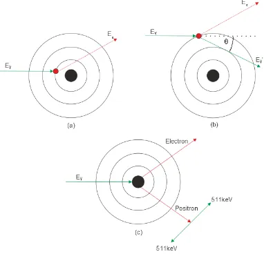
Figure 2.2: Illustration of the main gamma-ray interaction mechanisims that occur with matter. (a) shows photoelectric absorption, (b) is Compton scattering and (c) is pair production. Red lines indicate particle movement, green lines areγ rays.
2.2.2 Compton scattering
Compton scattering occurs when an incident gamma ray interacts with a weakly bound
atomic electron, transferring a fraction of its energy and subsequently the gamma ray
transferred to the electronEedepends upon the gamma-ray scattering angle, it retains
an energyEγ0. Assuming the electron is initially at rest and unbound, with a rest mass of mec2 = 511keV, Equation 2.3 can be derived from the conservation of energy and
momentum.
Eγ0 = Eγ 1 + Eγ
mec2(1−cosθ)
(2.3)
The scattering angle can vary up to 180 degrees where the maximum energy transfer
occurs. This gives a range of energies for Eγ0 and Ee. In reality the recoil electron is not initially at rest, it is bound to an atom and moving within an atomic orbital. This
results in a further spread of energies called Doppler broadening. This effect is more
prominent when the absorbing material has a highZ and also for lower energy incident gamma rays [14].
To predict the angular distribution for scattered gamma rays a differential scattering
cross section ddσΩ can be used, this is the Klein-Nishina distribution as described by Equation 2.4.
dσ dΩ =Zr
2 0
1
1 +α(1−cosθ)
2 1 +cos2θ
2
!
1 + α
2(1−cosθ)2
(1 +cos2θ)[1 +α(1−cosθ)]
!
(2.4)
where
α = Eγ
mec2
(2.5)
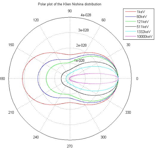
Figure 2.3 represents this graphically as a polar plot of the number of gamma
rays scattered at an angle θ for different gamma-ray energies. It can be seen that higher gamma-ray energies are preferentially scattered in a forward direction, while
lower energy gamma-rays are scattered in a more symmetrical distribution about the
90 degree axis.
The probability of a Compton scatter increases linearly as the Z of the scattering material increases due to the number of target electrons increasing linearly with Z. Compton scattering is the dominant process within the energy range of 0.2 to 6 MeV
in germanium as shown in Figure 2.1, this range is wider for silicon, going from 0.06 to
19 MeV.
2.2.3 Pair production
Pair production occurs when an incident gamma ray interacts within the Coulomb field
of a nucleus and disappears. The gamma ray is replaced by an electron-positron pair as
shown in Figure 2.2(c). By the conservation of energy this process can only occur if the
incident gamma ray has energy sufficient to create an electron-positron pair. Assuming
Figure 2.3: The Klein Nishina distribution shows that for higher energy gamma rays it is more probable that they will Compton scatter in a forward direction. For energies around 10MeV the gamma rays are preferentially scattered in a forward direction where as for energies less than 100keV the distribution becomes more symmetrical about the 90 degree axis.
1.022MeV. Any additional energy from the gamma ray is shared between the pair as
kinetic energy. The positron will travel through the material, thermalising as it goes
until it annihilates with an electron within the material producing two 511keV gamma
rays at 180 degrees from each other assuming the electron and positron are both at
rest. A small variation in energies and angles is seen in actuality due to the momentum
of both particles. These two gamma rays can be absorbed within the material although
one or both may escape, resulting in escape peaks being visible in gamma-ray spectra
[15].
2.2.4 Linear attenuation coefficient
A material’s ability to absorb an incident gamma ray’s energy completely is defined by
its linear attenuation coefficient,µ. Its measured for a given gamma-ray energy and is a property of the material. The relationship for a fixed energy is given in Equation 2.6.
µtotal=µP A+µCS+µP P (2.6)
where the attenuation for each interaction is taken individually,µP A is the attenuation
If a monoenergetic beam of gamma rays is incident on a material, the intensity I
measured after a thickness of materialzis given by Equation 2.7, where I0is the initial
beam intensity.
I =I0eµtotalz (2.7)
2.3
Interactions of charged particles with matter
Electrons can be emitted from atoms during the processes described previously. Within
a semiconductor detector electrons are one of the charge carriers of interest.
Under-standing how these particles interact with material is therefore a vital part of
under-standing the workings of a semiconductor gamma-ray detector.
Unlike gamma rays which lose energy via discrete processes, electrons lose energy
continuously as they travel through a material via collisions with other electrons and by
emitting radiation. Energy losses due to collisionsdEdx
cand losses due to the emission
of radiationdEdx
r combine to give the linear stopping power
dE dx
total for a material
for electrons and as given in Equation 2.8.
dE dx total = dE dx c + dE dx r (2.8)
2.3.1 Collisional energy loss
Electrons travel through a material, Coulomb scattering via elastic and inelastic
meth-ods from bound atomic electrons. The energy loss for an electron with velocity v
incident on a material with atomic numberZ and density N can be described by the collisional Bethe-Bloch formula,
−
dE
dx
c
= 2πe
4N Z
m0v2
ln
"
m0v2E
2I2k
#!
(2.9)
where
k= 1−β2 (2.10)
β = v
c (2.11)
and I represents the average excitation and ionisation that takes place with each collision.
2.3.2 Radiative energy loss
Electrons entering the Coulomb field of a nucleus will be decelerated and deflected
spectrum of photons is seen as the energy is transferred. These photons can be absorbed
within the material or if they have enough energy they can escape. The energy loss
of electrons due to this radiation emission is described by the radiative Bethe-Bloch
formula, Equation 2.12 (this equation uses the same notation as Equation 2.9).
−
dE
dx
r
= N EZ(Z+ 1)e
4
137m2 0c4
4ln
2E
m0c2
− 4
3
(2.12)
The energy loss caused by radiative means is less than that from collisions for an
electron kinetic energy below 1MeV. The ratio of the energy losses seen from both
processes can be seen in Equation 2.13.
dE dx r dE dx c ≈ EZ 700 (2.13)
Radiative losses are only significant if the material has a high Z value or if the electron energy is in the MeV or above range. This thesis will concentrate on materials
withZ of 14 (silicon) and 32 (germanium) along with gamma-ray energies of 1.332MeV and below. Radiative energy loss for the electrons will therefore be minimal.
2.4
Solid state gamma-ray detectors
Gamma rays interact with the material of a detector via the processes described
pre-viously. Energy is transferred to the electrons within the material from the incident
gamma rays. The electrons subsequently transfer their energy into the bulk of the
material via exciting other electrons, ionising atoms or emitting Bremsstrahlung
ra-diation until they come to rest. The resulting net charge deposition can be detected
as an electrical signal, this is processed through electronics to produce the gamma-ray
spectra of interest. Solid state gamma-ray detectors fall into two distinct categories,
either scintillators where a light pulse is produced for each gamma-ray interaction or
semiconductor diodes where electron-hole pairs are produced.
2.4.1 Semiconductors
Typically materials are separated into three categories, conductors, insulators or
semi-conductors. The separation depends upon the occupation of energy bands by the
electrons within the material. A simplified view assumes that there are two bands, the
valence and conduction bands, separated by a forbidden region which no electrons will
occupy, the band gap. The valence band corresponds to outer shell electrons bound to
specific lattice sites within the crystal, creating part of the covalent bonding forming the
inter-atomic forces within the crystal. The conduction band contains electrons that are
free to migrate through the material and which contribute to the material’s electrical
![Table 2.1: Properties of intrinsic silicon and germanium, from [15]](https://thumb-us.123doks.com/thumbv2/123dok_us/8064018.226406/39.612.221.411.135.316/table-properties-intrinsic-silicon-germanium.webp)
![Figure 2.15: Schematic representation of the weighting field within a strip detector,reproduced from [23]](https://thumb-us.123doks.com/thumbv2/123dok_us/8064018.226406/52.612.209.432.70.287/figure-schematic-representation-weighting-eld-strip-detector-reproduced.webp)