i
The Silver, Copper and
Silicon(110) Surfaces
in Ambient Environments
Thesis submitted in accordance with the requirements of the University of Liverpool for the degree of Doctor in Philosophy by
Elizabeth Emily Barritt
Department of Physics
ii
The Silver, Copper and Silicon(110) Surfaces in Ambient
Environments
Elizabeth Emily Barritt
Abstract
The results presented in this thesis were part of a research programme that utilised the surface sensitive technique reflection anisotropy spectroscopy (RAS) to study the silver, copper and silicon (110) surfaces under ambient conditions.
It has been shown that although the preparation of these surfaces can be less precise in ambient conditions, than when prepared in an ultra high vacuum (UHV) environment, the main features observed are similar. The features observed in the RA spectrum for the Si(110) surface in ambient conditions show good agreement with previous data performed in a UHV environment. The experiments performed using the Ag(110) surface show that when the Ag(110) crystal is heated to higher temperatures, when the oxide present will have dissociated off the surface, the ambient RA spectrum shows good agreement with experiments performed in UHV. However, the transition between surface states observed in UHV was not seen in the RA spectrum in ambient conditions. These experiments were performed using the part of the RA spectra. However, to examine the surfaces further the
part of the RA spectra was also presented along with the azimuthal dependence of the RA spectrum.
iii
Acknowledgements
I would like to begin by thanking Peter Weightman for his constant support and enthusiasm over the past four years. His knowledge of the subject and many areas surrounding it has provided me with a continuous standard to strive to reach and further progress my own knowledge. I would also like to thank Trevor Farrell, his increased support and guidance over the last two years have been vital and without it this thesis would not have been possible. It has been an honour to work alongside many distinguished scientists in our research group, Caroline Smith, Paul Harrison and Andrew Bowfield and also the past and present PhD students, Gareth Holder, James Convery and Tim Craig who have provided friendship and support over many tea breaks!
I would also like to thank my current work collegues, Caroline Shenton-Taylor, Doug Blackie, Wayne Harrison, Joe Watson and Kelly Vaughan for their support and friendship since I started work.
v
Acronyms
ADRAS Azimuth Dependent Reflection Anisotropy Spectroscopy AFM Atomic Force Microscopy
BZ Brillouin Zone
CD Circular Dichroism
DVM Digital Voltmeter
ERS Electroreflectance Spectroscopy
FCC Face Centred Cubic
FFT Fast Fourier Transform
IHP Inner Helmholtz Plane
IR Infra-Red
LED Light Emitting Diode
LEED Low Energy Electron Diffraction OHP Outer Helmholtz Plane
PEM Photoelastic Modulator PMT Photomultiplier Tube PZC Potential of Zero Charge
RAS Reflection Anisotropy Spectroscopy RDS Reflection Difference Spectroscopy SBZ Surface Brillouin Zone
SCE Standard Calomel Electrode SDA Surface Dielectric Anisotropy SE Spectroscopic Ellipsometry SLFE Surface Local Field Effect
SPR Surface Plasmon Resonance
STM Scanning Tunnelling Microscopy SXS Surface X-ray Scattering
vi
UV Ultra Violet
XPS X-Ray Photoelectron Spectroscopy
vii
Contents
Chapter 1
Introduction
11.1 Introduction 2
1.2 Surface Science outside Ultra High Vacuum 3
1.3 Thesis Aims 4
1.4 Thesis Structure 4
1.5 References
6
Chapter 2
Theory
82.1 Crystal Structure 9
2.1.1 The Reciprocal Lattice and Brillouin Zones 10
2.2 Band Structure 11
2.2.1 Free Electron Fermi Gas 12
2.2.2 Electronic Band Structure of Solids 13
2.2.3 Band Structure in Metals 15
2.2.4 Semiconductor Band Structure 16
2.3 Surfaces 17
2.3.1 Surface Phase Transitions 17
2.3.2 Transitions between Surface States 18
2.3.3 Surface Brillouin Zone 19
2.3.4 Optical Response of Surfaces 20
2.3.5 Plasma Frequency 22
2.4 The Three Phase Model 25
2.5 References 27
Chapter 3
Experimental Set Up
283.1 Reflection Anisotropy Spectroscopy 29
3.1.1 The RA Spectrometer and its Components 30
3.2 Propagation of Light through the System 35
3.2.1 Errors 44
3.3 Azimuthal Dependent Reflection Anisotropy
viii
3.4 Electrochemistry 49
3.4.1 Measuring Electrode Potential 52
3.4.2 The Electrochemical Cell 53
3.4.3 Cyclic Voltammetry 54
3.5 Crystal Preparation 55
3.6 Low Energy Electron Diffraction and X-ray
Photoelectron Spectroscopy 57
3.6.1 Low Energy Electron Diffraction 58
3.6.2 X-ray Photoelectron Spectroscopy 58
3.7 References
60
Chapter 4
The Si(110) Surface
634.1 Introduction 64
4.2 The Physical Structure of Silicon 64
4.3 The Electronic Structure of Silicon 65
4.3.1 The Electronic Structure of Si(110) 68
4.4 Interband Transitions 69
4.4.1 Temperature Dependence of Interband
Transitions 72
4.5 The Reflection Anisotropy Spectroscopy of the
Si(110) Surface 76
4.5.1 The
part of the RA Spectra as a
function of temperature 76
4.5.2 The
part of the RA Spectra as a
function of temperature 80
4.6 The Complex Anisotropic Surface Dielectric
Function of Si(110) 84
4.7 Summary 91
4.8 References 92
Chapter 5
The Ag(110) Surface
955.1 Introduction 96
5.2 Ellingham Diagram for Silver 96
ix 5.3.1 The Electronic Structure of the Ag(110)
Surface 99
5.3.2 Reflection Anisotropy Spectroscopy of the
Ag(110) Surface in UHV 100
5.3.3 The Temperature Dependence of the Ag(110)
Surface 103
5.3.4
The Azimuthal Dependent Reflection Anisotropy Spectroscopy of the Ag(110) Surface
104
5.4 The Reflection Anisotropy Spectroscopy of the
Ag(110) Surface 109
5.4.1 The part of the RA Spectra 109
5.4.2 The
part of the RA Spectra as a
function of temperature 111
5.4.3 The
part of the RA Spectra as a
function of temperature 116
5.5 Azimuthal Dependence of the Ag(110) Surface 120
5.6 Summary 124
5.7 References 126
Chapter 6
The Cu(110) Surface
1286.1 Introduction 129
6.2 The Physical Structure of the Cu(110) Surface 129
6.3 The Electronic Structure of Copper 131
6.3.1 The Electronic Structure of the Cu(110)
Surface 132
6.4 Reflection Anisotropy Spectroscopy of the
Cu(110) Surface 134
6.4.1 Reflection Anisotropy Spectroscopy as a
Monitor of Surface States 137
6.5 The Metal/Liquid Interface 141
6.5.1 Surface States at the Metal/Liquid Interface 142 6.5.2 Reflection Anisotropy Spectroscopy of the
Metal/Liquid Interface 142
6.6 The Cu(110)/Liquid Interface 143
x H2SO4 solutions
6.6.2 The Cu(110)/Liquid Interface using 5 mM H2SO4 + 10 mM KBr solution
146
6.6.3 The Cu(110)/Liquid Interface using 10 mM HCl
solution 148
6.6.4 Kinetic Spectra of the Cu(110) Surface using
10 mM HCl solution 154
6.7 Azimuthal Dependence Reflection Anisotropy
Spectroscopy of the Cu(110)/HCl Interface 157
6.8 Summary 160
6.9 References 162
Chapter 7
Conclusions
1677.1 Conclusions 168
7.1.1 Conclusions on Si(110) 168
7.1.2 Conclusions on Ag(110) 169
7.1.3 Conclusions on Cu(110) 170
7.2 Future Work 171
1
Chapter 1
2
1.1 Introduction
For centuries, mankind has pushed the boundaries of science to invent, to discover and to create, some of the most pioneering advancements that are often taken for granted in the 21st century. From Galileo’s initial understanding of gravity in the late 16th century to the discovery of penicillin by Fleming in the 1920’s there is an underlying trend spanning throughout the centuries, that of human curiosity. Although many of these advancements have had a huge practical impact on the current world, such as the inventions of the steam engine or telephone, they all begin with an idea, a natural impulse to push the limits of human understanding into the realms of impossibility. The last two centuries provided some of the great industrial advances along with domestic luxuries such as the television, the computer and the electric washing machine, present in almost every home. Moving forward into the current century and the emphasis has been on upgrading, screens with ever increasing definition to give one example. Accessibility of information has also been improved with Ofcom [1] stating that smart phone intake has risen to 39 % in 2012 compared to 27 % in 2011. This high rate of increase in household electronics is a result of electric components, such as transistors, decreasing in size and the research is progressing further to investigate single molecule electronics [2]. However, advancing into this area requires interdisciplinary collaborations which are becoming the norm across all scientific research groups.
3 Au(110) surface been well understood at the solid/liquid interface [6]. However, it would be useful to have a more complete knowledge of the surface outside a UHV environment and to observe if the surface retains all the same properties outside the UHV chamber.
1.2 Surface Science outside Ultra High Vacuum
The development of surface science, and crystallography in general, increased rapidly through the mid to late 20th century [7-9] partly due to the ability to maintain the pressures required inside the UHV chamber at a constant level. This aided the development of many techniques, such as LEED [10], STM [11] and XPS [12], which capitalised on the lack of contaminants present in the chamber by using electrons and x-rays to probe the surface structure of many materials. However, to probe the surfaces in a non-UHV environment other techniques are utilised, in particular those which use photons to probe the surface, which are more suitable to be used in atmosphere. For example, the experimental technique reflection anisotropy spectroscopy (RAS) has been used to study materials in both UHV and non-UHV environments and it also has the ability to study the metal/liquid interface. This, combined with the ability of RAS to monitor changes on the surface, such as a when a molecule has been adsorbed, makes it a very useful technique when studying surfaces outside UHV whilst being able to compare results with the same surface studied inside UHV.
When studying clean surfaces in a non-UHV environment their possible oxidation needs to be taken into account. With some surfaces this can be done by heating the surface so the oxide layer dissociates from the surface. However, with others this process needs to be performed electrochemically.
4 electrolyte is the site of many crucial interactions which will aid both scientific development and industrial research.
1.3 Thesis Aims
The research presented in this thesis will show the results from experiments performed in a non-UHV environment, either in air or at the solid/liquid interface. This thesis uses the Si(110), Ag(110) and Cu(110) surfaces which are all well understood in UHV environments so the RAS results obtained in non-UHV environments can be compared with previous results. Understanding how the surfaces behave in non-UHV environments will further the understanding of surface science research and could aid in the development of practical applications.
1.4 Thesis Structure
This thesis will begin with a brief background discussion on some of the main scientific theories and concepts which will provide a basis for the rest of the research before moving on to describe the experimental set up. This chapter will detail the RA spectrometer, explaining all the individual components, which will then proceed to describe how the light propagates through the entire system.
The thesis will then go on to investigate the results obtained from the three surfaces studied. The following three chapters will be self-contained and therefore each one will begin with a description of the material and its properties before going on to present the results.
Initially the research will focus on the Si(110) surface studied in air. This chapter will centre around the dependence on the main features in the RA spectrum with increasing temperature. These features coincide with particular transitions in the electronic band structure of silicon.
5 on the surface in an atmospheric environment. The main feature in the RA spectrum coincides with the plasmon resonance energy and the azimuthal dependence of the surface at the plasmon resonance energy is different from that observed at other energies within the RA spectrum. Although this dependence is seen clearly in the experiments from a UHV environment, when studied in air, this dependence is not observed. However, evidence presented in this thesis suggests the Ag(110) surface behaves in a similar way as in UHV.
The final results chapter moves away from atmospheric conditions and focuses on the Cu(110)/electrolyte interface. This experiment involves an electropolishing technique to prepare the surface followed by electrochemistry to manipulate the adsorption and desorption of molecules present in the electrolyte. Therefore, it is possible to observe the clean Cu(110) surface and compare with the well understood Cu(110) surface in UHV. The results presented show good agreement with the UHV data, in particular a surface state observed in UHV on the Cu(110) surface is also present on the Cu(110) surface in an electrolyte, although it has been shifted to slightly higher energy.
6
1.5 References
[1] Ofcom 2012. ‘Communications Market Report 2012’ [online] available at: http://stakeholders.ofcom.org.uk/binaries/research/cmr/cmr12/CMR_UK_
2012.pdf
Date accessed 12/04/2013
[2] Joachim, C., Gimzewski, J. K. and Aviram, A., Nature 408 (2000) 541
[3] Smith, C. I.,Bowfield, A., Dolan, G. J.,Cuquerella, M. C., Mansley, C. P., Fernig, D. G., Edwards, C. and Weightman, P., J. Chem. Phys. 130 (2009) 044702
[4] Convery, J. H., Smith, C. I., Khara, B., Scrutton, N. S., Harrison, P., Farrell, T., Martin, D. S. and Weightman, P., Phys. Rev. E. 86 (2012) 011903
[5] Weightman, P., Martin, D. S., Cole, R. J. and Farrell, T., Rep. Prog. Phys. 68 (2005) 1251
[6] Smith, C. I., Harrison, P., Farrell, T. and Weightman, P., J. Phys: Condens. Matter 24 (2012) 482002
[7] McGilp, J. F. Prog. Surf. Sci. 49 (1995) 1 [8] Woodruff, D. P., Surf. Sci. 500 (2002) 147
[9] Hodeau, J. L. and Guinebretiere, R. Appl. Phys. A-Mater. 89 (2007) 813 [10] Jona, F., Strozier, J. A. and Yang, W. S., Rep. Prog. Phys. 45 (1982) 527
[11] Binning, G., Rohrer, H., Gerber, Ch. and Weibel, E., Phys. Rev. Lett. 49 (1982) 57
7 [13] Bockris, J. O’M. And Khan, S. U. M., Surface Electrochemistry: A molecular
level approach. (Springer, New York) 1993
[14] Soriaga, M. P., Prog. Surf. Sci. 39 (1992) 325
8
Chapter 2
9
2.1 Crystal Structure
To understand the fundamental properties of materials such as silicon, silver and copper which this research focuses on, it is important to know the basic crystal structure of the material. Crystals are made up of identical building blocks arranged in a three dimension array. These building blocks can be either atoms or small identical groups which are located on a set of mathematical points called the lattice which then give the crystal structure. In three dimensions there are 14 different lattice types which are called Bravais lattices which are allocated to subgroups depending on the cell axes and angles. This research focuses on the cubic group in which all the cell axes are of equal length (a1 = a2 = a3) and all angles between them are equal to 90 ° shown in figure 2.1. The three lattice types within the cubic group are simple cubic (sc), body centred cubic (bcc) and face centred cubic (fcc) of which the latter is the one this research focuses on.
Figure 2.1: The cubic lattice group with (a) the simple cubic, (b) the body centred cubic and (c) the face centred cubic.
10 2.1.1 The Reciprocal Lattice and Brillouin Zones
The reciprocal lattice is the Fourier transform of the real space initial lattice and is used to further describe the crystal structure. It also allows the introduction of Brillouin zones which are defined as Wigner-Seitz primitive cells in reciprocal space. It is important to have an understanding of Brillouin zones since they play an important role when discussing the electronic band structure of crystals [1]. The zone boundaries are specified by planes bisecting the lines joining neighbouring lattice points. These planes satisfy the equation for Bragg’s law:
[image:20.595.240.399.371.536.2]
Hence the construction of a Brillouin zone exhibits all the wavevectors which can be Bragg reflected. The construction is shown in figure 2.2.
Figure 2.2: A square reciprocal lattice with the black lines representing reciprocal lattice vectors, white lines show the perpendicular bisectors of the reciprocal lattice vectors. The shaded central
square shows the Wigner-Seitz cell of the reciprocal lattice called the first Brillouin zone [1].
As shown in figure 2.2 the first Brillouin zone is the shaded central square but there are also higher orders of Brillouin zones further away from the origin. The higher order Brillouin zones are shown more clearly in figure 2.3 without the extra construction lines. The first Brillouin boundary occurs at:
(2.1)
(2.2) This text box is where the
unabridged thesis included the following third copyright material:
11 where k is the wavevector and a is the spacing between the planes.
Figure 2.3: Schematic of the first four Brillouin zones. The first Brillouin zone has boundaries at ± π/a [2].
The Brillouin zones are expanded into three dimensions for a three dimensional lattice, although the illustrations of them become more difficult as seen in figure 2.4 for a fcc lattice. The letters shown in figure 2.4 are the high symmetry points of the Brillouin zone with Γ generally shown as the centre.
Figure 2.4: First Brillouin zone for a fcc lattice [3].
2.2 Band Structure
Until now the discussion has focused on the crystal lattice but another important factor is the movement of electrons through the lattice. To begin with the free electron model is introduced, which describes the motion of electrons in free
This text box is where the unabridged thesis included the following third copyright material:
Hummel, R. E., Electronic Properties of Materials, Fourth Edition. (Springer, New York) 2011
This text box is where the unabridged thesis included the following third copyright material:
12 space, and then the discussion will focus on how it has been adapted to give a more realistic view of the electron motion. This will then facilitate how band structures have been understood in the context of specific materials.
2.2.1 Free Electron Fermi Gas
The free electron gas is a simple model used to describe the kinetic properties of electrons. The Schrodinger equation that describes a free particle in three dimensions is given by:
where ħ is the reduced Planck’s constant, m is the mass of the electron, ψk(r) is a
wavefunction with wavevector k and εk is the energy of the electron in the orbital.
If the electrons are confined within a cube with length L then the wavefunctions which satisfy equation 2.3 are given by a travelling plane wave since the wavefunction must be periodic in all three dimensions with period L:
provided the x, y and z components for k satisfy:
Since the wavefunction, ψk(r), represents a travelling wave this means they will
also carry momentum which is given by:
The energy, εk, can be found by substituting the wavefunction in equation 2.4 into
the Schrodinger equation in equation 2.3:
(2.3)
(2.4)
(2.5)
(2.6)
13 where k is the wavevector in all three dimensions. The Fermi energy can then be related to equation 2.7 since for N electrons in the ground state the occupied orbitals can be described as points within a sphere in k space. This sphere will have a radius equal to the wavevector, kF, and so the energy at the Fermi surface will be given by:
The Fermi surface is the surface at constant energy, εF, in k space and it is important when discussing the electrical properties of metals since it describes the changes of occupancy of states near the Fermi surface.
2.2.2 Electronic Band Structure of Solids
As mentioned the free electron Fermi gas is just a model and in reality the assumptions of a one-electron system are too simplistic. For example the free electron model does not provide information into the differences between metals, semiconductors and insulators. To understand further the model needs to be expanded for a solid where the atoms will be more closely packed together. By adding the periodic lattice of the solid, the free electron model becomes the nearly free electron model. Since Bragg reflection occurs in a crystal lattice by monitoring where the reflection takes place, energy gaps are observed. The information gained from energy gaps can then be used to determine the differences between a metal, insulator and semiconductor. The first energy gap occurs at the first Bragg reflection and at integer values thereafter, giving:
This is equal to the boundary conditions for the first Brillouin zone when n = 1 as shown in equation 2.2 although energy gaps will occur at integer values of n. The differences in the free electron model and when the lattice potential has been added are shown in figure 2.5. As seen in the diagram the relationship between the
(2.8)
14 energy and wavevector in the free electron case is a parabola whereas the case when the electron is not free shows band gaps. The band gaps occur because as the wavevector approaches the condition in equation 2.9 reflected waves will appear and when the condition is reached there will be equal forward and backward components of the wavefuction leading to standing waves. The two standing waves which are formed are:
where and are the two travelling waves. Since it is not possible to construct a wavefunction which represents an electron state with an energy between the energies of the electron states associated with the wavefunctions in equations 2.10 and 2.11 there will be a gap in the allowed electron states. Hence the energy gap, Eg, will be the difference in energies of ψ+ and ψ-. Just below the energy gap the wavefunction will be ψ+ whereas above the wavefunction will be ψ -[4] as shown in figure 2.5.
Figure 2.5: Plot of energy, ε, against wavevector, k, for (a) a free electron and for (b) a nearly free electron with lattice constant, a.
15 this region. The extended zone scheme is only applicable for the free electron case and ε is plotted as a single value function from minus to plus infinity. The reduced zone scheme is then set up using Fourier expansions and solving the Schrodinger equation in k space. This would result in multiple solutions for ε with k in the first zone and in the second zone the solutions would have all the same ε values repeated. Therefore it is concluded that the first zone would give all the information required.
2.2.3 Band Structure in Metals
The relative differences in electron occupancy of the energy states allowed in metals, semiconductors and insulators are shown in figure 2.6. The Fermi energy is not shown since it occurs at the boundary of the occupied and unoccupied states for the metal. For the insulator it would occur in the band gap between the occupied and unoccupied energy bands. The semiconductor is a little more complicated since there is more free movement of electrons between the two mainly occupied or mainly unoccupied energy bands but the Fermi energy would again lie in the band gap between these two zones.
Figure 2.6: Schematic diagram of the allowed energy bands of an insulator, metal and semiconductor. The shaded regions are filled with electrons whereas the white areas are not.
16 in figure 2.6 where no electron states occur. However, in the band there will be delocalised electron states which show translational invariance. Felix Bloch in 1928 proved that within the periodicity of a crystal lattice the wavefunction for a periodic potential will be the product of a plane wave with another function with the periodicity of the lattice:
Transitions between band states are possible if selection rules allow it.
2.2.4 Semiconductor Band Structure
Semiconductors are vitally important in many applications such as photovoltaic cells, transistors and light emitting diodes (LED’s). Therefore understanding their structure and behaviour is the aim of many scientific studies. In general semiconductors have an electrical resistivity in the range of 10-2 to 109 Ωcm and this is temperature dependent. Semiconductors can be pure elements, such as germanium and silicon, be binary compounds such as gallium arsenide, or even organic materials. An intrinsic semiconductor is one which has not been doped with a foreign species so the conductivity, or number of charge carriers, relate to the material properties itself rather than impurities of another material. The electrical resistivity of semiconductors is temperature dependent and when at absolute zero they will generally be insulators and the conduction band will be empty of electrons. The gap between the conduction band and valence band is called the band gap and is material specific. Once the temperature is increased electrons can move from the valence to the conduction band due to the thermal excitation leaving behind holes (unoccupied states). It is this basic principle which explains why the resistivity of semiconductors is highly temperature dependent. The ability for valence electrons to move across the band gap depends not only on the size of the band gap but also the temperature. This can be expressed as a ratio which determines the carrier concentration:
17 where kB is Boltzmann’s constant. If this ratio is small, the carrier concentration in the conduction band will be large and so will the conductivity. These band gaps can also be direct or indirect which means either the maxima of the valence band and minima of the conduction band occur at the same value of k or at different values of k. In this research silicon is used and this has an indirect band gap with a band gap energy of 1.17 eV at 0 K or 1.11 eV at 300 K [1].
2.3 Surfaces
The previous analysis has focused on the general properties of solids and the bulk structure of the material. However, the main aspect of this research is concerned with the surface behaviour of materials which will now be covered in more detail.
Surfaces are different to the bulk material since there is not the three dimensional periodicity that is found within the bulk. There is a smaller interatomic spacing for the topmost three layers of atoms (approximately) which can cause the surface layer to ‘relax’ although often keeping the same symmetry of the projection of the bulk on to the surface. However, if the surface of the material is compatible with different primitive cells to the bulk then the surface may have reconstructed to a more energetically favourable structure. For example, under UHV conditions, Au(110) has a (1x2) reconstruction on the surface whereas Cu(110) and Ag(110) maintain a (1x1) structure. The stabilisation of the (1x2) structure of the Au(110) surface is thought to be due to the need to lower the kinetic energy of the electrons in the s and p electron orbitals at the surface by delocalisation.
2.3.1 Surface Phase Transitions
Phase transitions are present in many systems and can be classified as either first or second order transitions. First order transitions include the solid/liquid/gas transitions which involve a latent heat. Second order transitions are continuous
18 transitions that at thermodynamic equilibrium (at constant temperature and volume) minimise their free energy, F.
where U is the internal energy, T is the temperature and S is the entropy of the system. These second order transitions will occur at specific temperatures when the free energy, F, can be divided between the internal energy, U, and the entropy,
S. When a transition takes place there will be a change of order in the system and ‘order parameters’ are defined when the transition temperature, TC, is reached. The order parameter changes with (T – TC) β,where β is the critical exponent and only depends on the dimensionality of the order parameter, the dimensionality of space and the symmetry of the system.
2.3.2 Transitions between Surface States
There are two types of electronic states which are associated with the surface atoms [7], surface resonances and surface states. Surface resonances are located mainly at the surface although there can be some interaction with the bulk since their energies overlap with the bulk bonds. Surface states are localised at the surface and have energies within in the bulk energy gap. Figure 2.7 shows the projected bulk band structure at the surface of a metal where is a two dimensional wavevector. The vector characterises a surface Brillouin zone which is similar to the bulk Brillouin zone but on the surface and so the rod then extends into the bulk Brillouin zone. The two lines in the band gaps represent where surface states could be present on the surface but not present in the bulk. Since these surface states (resonances) are present for a number of values the states look like a band of states. When this band of states interacts with the projected bulk of the material this bulk state will possess a large amplitude on the surface resulting in a surface resonance.
19
Figure 2.7: Schematic diagram of the bulk band structure at the surface of a metal [8].
2.3.3 Surface Brillouin Zone
As mentioned the surface Brillouin zone will be the projection of the bulk states onto the surface. Figure 2.4 shows a three dimensional fcc Brillouin zone and if a cross sectional slice is taken through it the corresponding surface Brillouin zones can be observed as shown in figure 2.8.
Figure 2.8: Cross section through an fcc bulk Brillouin zones and the projections onto surfaces [9].
Where the notation of letters are determined by the high symmetry points of the bulk Brillouin zone, as mentioned earlier, but the lines above the letters
This text box is where the unabridged thesis included the following third copyright material:
Zangwill, A., Physics at Surfaces. (Cambridge University Press, Cambridge) 1988
This text box is where the unabridged thesis included the following third copyright material:
Goldmann, A., Dose, V. and Borstel, G., Phys. Rev. B 32
20 representing the surface Brillouin zones denote that these have a two dimensional character.
2.3.4 Optical Response of Surfaces
The dielectric function ε(ω, k), describes the interaction of light, or electromagnetic radiation in general, with a material. It is an important property which is strongly influenced by the crystal structure since it is very sensitive to changes in the band structure. This means that the study of how the dielectric function changes, can yield insight into the band structure of a material. However, the dielectric function cannot be measured directly so techniques such as reflectivity measurements are used. Although the dielectric function depends on the frequency, ω, and the wavevector, k, of the radiation, during the infrared, visible and ultraviolet regions of the electromagnetic scale the wavevector is very small compared to the frequency and can be treated as zero. The dielectric function, ε(ω) is a complex function and so will have the form as shown in equation 2.15.
Throughout the rest of this thesis the dielectric function will be written just as ε,
with the real and imaginary parts written as ε’ and ε’’ respectively. Similarly, equation 2.15 can also be written as a subtraction between the real and imaginary parts of the dielectric function although the notation throughout this thesis will be the addition of these two terms.
This research focuses on electromagnetic radiation in the visible spectrum and under relatively low intensities so the induced electric polarisation in the material is given by:
where ε0 is the dielectric permittivity of free space and χ(1) is the first order susceptibility. χ(1) measures the degree of polarisation from an incoming electric field and is given by:
(2.15)
21
where ε is the complex dielectric function shown in equation 2.15.
The complex dielectric function, ε, cannot be measured directly but using functions such as the reflectance, R, the refractive index, n, and the extinction coefficient, K, information can be obtained. One of the best experimental techniques to obtain information of the dielectric function is to use reflectivity from a surface at normal incidence. The reflectivity coefficient, r, is the ratio of reflected light, Eref, with incident light, Einc as shown below:
where r will also be a complex function which will depend on the refractive index,
n, and extinction coefficient, K, at normal incidence shown in equation 2.19.
This is related to the dielectric function using:
here N is the complex refractive index and is frequency dependent, explaining the absorption of light as it penetrates into the material.
Equation 2.20 can be solved for ε’ and ε’’ to give:
If the medium is weakly absorbing, K will be small so . The reflectivity, R, is then given by:
(2.17)
(2.18)
(2.19)
(2.20)
(2.21)
(2.22)
22 As mentioned earlier, this research uses a technique called reflection anisotropy spectroscopy (RAS) which is discussed in detail in chapter three but uses visible light reflection at near normal incidence and measures the fractional anisotropy in the reflectivity of a surface. Usually denoted as Δr/r where Δr is the difference in reflectance between two orthogonal directions, , and r is the mean reflectance.
2.3.5 Plasma Frequency
The induced electric polarisation in the material shown in equation 2.16 can also be written in terms of the displacement, D:
since the susceptibility, χ, is related to the dielectric function, ε, from equation 2.17.
When the number of fixed positive ions and free electrons are equal the solid can be treated like a plasma. In this system the free electrons are best described using a free electron gas model. For a displacement, x, the equation of motion of the electron is given by:
where x and E have a time dependence of the form where ω is the frequency of the light. Substituting this into equation 2.25 gives:
Therefore:
The single electron dipole moment is given by:
(2.24)
(2.25)
(2.26)
23
The polarisation can be defined as the dipole moment per unit volume which is written as:
where n is the number of electrons per unit volume.
Furthermore, equation 2.24 can be rearranged to give:
which, by substituting equation 2.29 into equation 2.30 gives:
This is the equation for the dielectric function of the free electron gas. If the plasma frequency is then defined as:
then equation 2.31 can be rewritten as:
The plasma frequency is a major determinant of the optical activity, absorbing or reflecting, of a material. Equation 2.20 shows how the complex refractive index, N, is related to the complex dielectric function, ε. Hence, when , , N will be imaginary whereas when , , N will be real and finally when
, . From equation 2.23 for the reflectivity, R, when , R will be unity.
R will decrease when and then approach zero when . Therefore, up (2.29)
(2.30)
(2.31)
(2.32)
24 to the plasma frequency, the reflectivity of a gas of free electrons will be at a maximum whereas after the plasma frequency the gas will absorb incident light.
When the dielectric function equals zero there are longitudinal frequencies of oscillation, ωL caused by a displacement, u, of the entire electron gas with respect to the fixed positive ions. A schematic of this process is shown in figure 2.9. At position (1) the free electron gas is around the fixed positive ions. However, if the entire gas is displaced the positive ions will exert a restoring force to oppose the displacement (2). Position (3) shows the ‘overshoot’ of the electron gas in the opposite direction resulting in a longitudinal oscillation. These oscillations are called the plasma oscillations where quantised oscillations are known as plasmons.
Figure 2.9: Schematic diagram showing the plasma oscillation with displacement u.
25
2.4 The Three Phase Model
Later, chapter three will describe the path of polarised light through the experimental RAS instrument. Here a three phase model is introduced to describe the changes in polarisation as the light is reflected from the surface. McIntyre and Aspnes [10] introduced a linear approximation that can be used for reflectivity calculations and developed the theory of the three layer model which was then progressed further by Cole et al [11]. This is shown schematically in figure 2.10.
Figure 2.10: Schematic diagram of the three phase model.
As shown in figure 2.10 the model is based on an anisotropic surface in between an isotropic semi-infinite bulk and an ambient/vacuum layer each with their own dielectric constants. The dielectric function of the anisotropic surface is split into two orthogonal directions, εsx and εsy. Due to the surface anisotropy these two values may not be equal so Δεs is referred to as the surface dielectric anisotropy (SDA). If it is assumed that the dielectric function of the ambient or vacuum is equal to one and the thin film approximation that d<<λ , the fractional anisotropy of the surface (Δr/r) can be given by equation 2.34 [10]. This will be a complex function as it is determined using the dielectric functions of the surface and bulk which are both complex quantities, as shown by the schematic diagram in figure 2.11.
26 However the bulk and surface dielectric functions are complex quantities as shown in figure 2.10 and by equations 2.35 and 2.36.
where and . So equation 2.34 can be written in
terms of its real and imaginary parts:
Although most studies using RAS have focused on the real part of the function, in this research some studies have been conducted using the imaginary part and the changes in the experimental set up will be discussed later.
Figure 2.11: Schematic diagram to show the complex dielectric functions.
(2.35) (2.36)
27
2.5 References
[1] Kittel, C., Introduction to Solid State Physics, Eighth Edition. (John Wiley & Sons Inc, Hoboken) 2005
[2] Hummel, R. E., Electronic Properties of Materials, Fourth Edition. (Springer, New York) 2011
[3] Myers, H. P., Introductory Solid State Physics, Second Edition. (Taylor & Francis, London) 1997
[4] Ibach, H. and Lüth, H., Solid State Physics, An Introduction to Principles of Materials Science, Fourth Edition. (Springer-Verlag, Berlin Heidelberg) 2009
[5] Alloul, H., Introduction to the Physics of Electrons in Solids. (Springer-Verlag, Berlin Heidelberg) 2011
[6] Ho, K. -M. and Bohnen, K. P., Phys. Rev. Lett. 59 (1987) 1833
[7] Kolasinski K. W., Surface Science: Foundations of Catalysis and Nanoscience, Third Edition. (John Wiley & Sons Inc, Chichester) 2012
[8] Zangwill, A., Physics at Surfaces. (Cambridge University Press, Cambridge) 1988
[9] Goldmann, A., Dose, V. and Borstel, G., Phys. Rev. B 32 (1985) 1971 [10] McIntyre, J. D. E. and Aspnes, D. E., Surf. Sci. 24 (1971) 417
28
Chapter 3
29
3.1 Reflection Anisotropy Spectroscopy
Reflection anisotropy spectroscopy (RAS) is a surface sensitive, non-destructive optical probe developed from spectroscopic ellipsometry (SE) [1,2]. The technique provides surface sensitive information by exploiting the anisotropy found at the surfaces of some cubic crystals. In many optical probes, the signal is dominated by contributions from the bulk since light can have a penetration depth of many tens of nanometres. In ultra high vacuum (UHV) systems sensitivity is obtained by exploiting the mean free path of electrons which can be up to 105 km in pressures of around 10-14 Pa compared to just 68 nm at ambient pressures. This corresponds to electron escape depths of 13 Å – 83 Å for energies in the region of 320 eV to 3.6 keV [3]. However, these techniques cannot be employed in ambient conditions due to the much shorter mean free path of electrons compared to UHV. RAS can be employed in ambient conditions and if the surface of a cubic crystal is anisotropic, reflectance will occur solely from the surface as the optical response from the bulk will be isotropic. This information is obtained by measuring the difference in reflectance (Δr) of normal incidence plane polarised light between two orthogonal directions in the surface plane, (x,y) then normalised to the mean reflectance (r):
where rx and ry are the complex Fresnel reflection coefficients of the two surface directions respectively.
Thus not only does RAS have the advantage of being non-destructive and surface sensitive, the technique can also be used under a wide range of environments providing they are optically transparent. This enables some of the limitations found in a UHV system to be overcome by expanding investigations of RAS to the solid/liquid interface and hence applications for electrode surfaces in electrochemical environments.
30 3.1.1 The RA Spectrometer and its Components
RAS shares some similarities with SE but there are differences which make RAS individual. Whereas in SE a sample is illuminated using linearly polarised light incident on the surface close the Brewster angle [4], RAS uses linearly polarised light to illuminate the sample at near normal incidence (≤ 5 °). The potential of RAS was developed in the 1980’s with the name reflection difference spectroscopy (RDS) by Aspnes and his co-workers [5] where studies focused on the growth of III-V semiconductors in near atmospheric pressures [6]. The further development of RAS progressed quickly through the following decades and has since been used to study surfaces in UHV and air [7], the metal/liquid interface in an electrochemical environment [8] and, more recently, has led to the study of the adsorption of biological molecules on the electrode surface [9-13]. A schematic diagram of the set up of the RA spectrometer is shown in figure 3.1 and the individual components are described in the order in that the light travels through them. Mirrors are not displayed in the schematic in figure 3.1 but are positioned before the polariser and after the analyser to facilitate focusing the light on the sample and then to ensure the maximum amount of light will progress into the detector..
Figure 3.1: Schematic of the basic components of the RA Spectrometer [7].
This text box is where the unabridged thesis included the following third copyright material:
31 Xenon Lamp
A Xenon lamp is used as the high intensity light source. Specifically it is a Hamamatsu 75 Watt Super-Quiet 9 Xenon arc discharge lamp, used in combination with a stabilised power supply (Hamamatsu C4621-02) which minimises fluctuations from the mains supply. The light radiated from the lamp is generated from an arc discharge when high voltages are applied across the anode to a high performance cathode within a xenon gas environment. Ideally, RAS needs a light source which has a sustainable output between the infrared (IR) and ultraviolet (UV) range (1.5-5.5 eV) of the electromagnetic spectrum which this lamp provides. Initially, when the lamp is switched on the xenon gas pressure can fluctuate preventing thermal equilibrium and hence maximum intensity from being reached. Experiments should only be performed after an hour as the lamp will then have reached a maximal and constant flux.
Mirrors
The mirror before the polariser, after the lamp, collects the light and focuses it on the sample. Then another mirror is placed after the analyser to ensure that as much light as possible is incident on the detector by introducing an astigmatism. This shapes the light beam into a narrow ellipse focused into the narrow entrance slit of the monochromator positioned immediately before the detector. The mirrors used in this set up are front coated UV enhanced aluminium on glass, with a thin silica coating to prevent mechanical abrasion.
Polariser
32 beam of light since they consist of two adjacent quartz prisms that separate the ordinary and extraordinary polarised beams which are polarised perpendicular to each other. By contrast Glan prism polarisers use total internal reflection to separate the polarised beams so only a single light beam emerges. This single beam set up is generally preferred in UHV experiments as the equipment can be kept more compact since there are no restrictions on the location of components in the optical layout. However, in this research Rochon prism polarisers are preferred as they are more efficient when transmitting light in the UV region. In this set up two beams emerge from the polariser so care must be taken to ensure the beams do not overlap.
Low Strain Window
The low strain window is used in electrochemical environments primarily due to the presence of the electrolyte solution in which the sample is fully submerged. The window will possess a small inhomogeneous birefringence and so there will be a small contribution from the window in the RAS signal. This can be removed by subtracting a corresponding spectrum from the experimental data. If an electrochemical set up is not being used and the light emerging from the polariser is directly incident on the sample there is no need for the window. There will still be a contribution to the RAS signal from the optical components in the set up not being 100% optically efficient so a corresponding spectrum should still be subtracted from the raw experimental data. The subtraction spectrum used was the difference spectrum between the initial spectrum and when the sample has been rotated by 90 °. Although this has a small effect when measuring the real part of the RA spectrum this subtraction is much more significant when measuring the imaginary part to enable the observation of all the features.
Photoelastic Modulator
33 sample by manipulating the property of stress induced birefringence. By applying an electric field to a piezoelectric crystal coupled to an appropriate transparent media, the PEM (specifically a Hinds Instruments Inc, PEM Quartz 90) induces an oscillating birefringence to the optical element which only affects the light linearly polarised parallel to the modulation. Hence leaving the light linearly polarised perpendicular to the modulation unchanged.
Here the transparent media used is fused silica. As the silica is compressed the light parallel to the modulation axis travels faster than the perpendicular component and vice-a-versa when the silica is stretched. This phase difference is called the retardation (Γ) and to achieve significant retardation the crystal is driven at its resonant frequency of 50 kHz, which also allows sequential resolution at the microsecond timescale to be obtained. Since the PEM modulates the phase this enables both the real and imaginary parts of the RA spectra to be measured.
Analyser
The analyser converts the phase modulated signal from the PEM into an amplitude modulated signal which can then be detected. It is of the same design as the polariser and so uses Rochon type prisms although in order to produce a modulated signal which switches between two linearly polarised states it must be orientated at 45 ° with respect to the polariser.
Monochromator
34 Detector
Directly behind the monochromator, to ensure the maximum amount of light enters, is a Hamamatsu (PMT Hamamatsu R955) multi-alkali cathode photomultiplier tube (PMT). The PMT is designed to measure the intensity of the incoming light and then converts the intensity modulated waveform into a current. Since the current is typically of the order of nanoamps the signal needs to be amplified before being converted into a voltage relative to the initial intensity of the light. The signal is made up of both an AC and a DC component. The AC component is related to the surface anisotropy and is superimposed onto a DC offset which is related to the reflectivity. To analyse these two components they are separated by a lock-in amplifier.
Other types of detector can be used, such as silicon photodiodes which are optimised for longer wavelengths, so in the UV range they perform poorly. To improve the performance in the UV range an appropriate coating can be applied which converts UV photons for detection within the visible spectrum. However, this coating reduces the sensitivity and so for this set up the PMT detector is used.
Lock-In Amplifier
In order to analyse the AC and DC components of the voltage signals separately a lock-in amplifier is used. The instrument used in this work uses an EG&G 5210 (dual-phase) lock-in amplifier manufactured by Perkin Elmer Instruments running at a frequency range of 0-120 kHz. By measuring the Fourier coefficients of the 1st and 2nd harmonics of the signal, the real and imaginary parts of the RA signal can be determined. By using a lock-in amplifier as described, signals at very specific frequencies can be detected which would otherwise be obscured by noise, which is necessary for the detection of the RA signal.
35 relationship as the signal. Hence, any differences between the frequencies of the signal of interest compared to this locked-in signal can be tracked. To achieve this, the locked-in reference signal is taken from the PEM.
3.2 Propagation of Light through the System
This section will explain how the light emitted from the Xenon lamp propagates through the instrument.
To understand the RA signal accurately a comprehensive method which can determine the state of polarisation of the light reflected from the surface of the sample is required. To begin with, the electric field vector, E, of a light wave that can be represented as the superposition of two orthogonal states is defined:
where,
and,
The resulting wave, E, is therefore the vector sum of components:
Where E0x and E0y are the amplitudes of the waves in the x and y directions respectively, k is the wavenumber, z is the position in space, ω is the angular frequency and t is time. Also δ = φx – φy and is the relative phase between the two components φx and φy which themselves are the phases of the x and y waves respectively.
The direction of polarisation of the resultant wave depends on its relative projection along each axis and also on δ. So when δ = mπ for m = 0, ±1, ±2... the
(3.2)
(3.3)
(3.4)
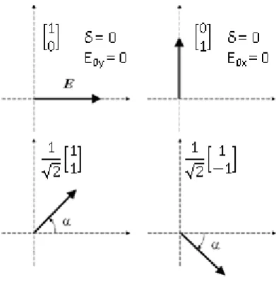
36 wave is linearly polarised as it is confined to one plane. For E0y = 0 or E0x = 0 the wave is then limited to vibrations along the x or y axis respectively. Hence, for non zero magnitudes, the linearly polarised light is inclined at an angle, α, to the x axis, shown in figure 3.2along with their corresponding Jones vector representations.
Figure 3.2: The common linear polarisation states.
To develop the theory further, the Jones vector notation needs to be introduced. The Jones vector notation was devised by Robert Clark Jones in 1941. It describes the state of polarisation of light in terms of the electric field vector and here it is used to discuss the propagation of light through the RA spectrometer. This notation is only valid for polarised light and although the light emitted from the Xenon lamp is unpolarised, once the light has progressed through the polariser it is observed in a definable polarisation state throughout the rest of the experimental system. Written in the notation of the Jones vector, the resulting wave E is:
where δx and δy are the appropriate phases and E0x and E0y are again the amplitudes of the waves in the x and y directions. Circular polarisation occurs if the magnitudes are equal, E0x = E0y, and out of phase by ± π/2. Although the magnitude
37 remains constant in this state, the direction of E changes with time following a circular path with angular frequency ω. This is shown in figure 3.3:
Figure 3.3: Circular polarisation states.
If the resultant vector also experiences a change in magnitude the result is a state of elliptical polarisation. Hence, when E0x ≠ E0y and the phase difference, δ, is a multiple of ± π/2, or it also occurs when E0x = E0y but the phase difference is an arbitrary angle. The elliptically polarised states are shown in figure 3.4 with (a) when δ = ± π/2 and E0x ≠ E0y and (b) when δ ≠ ± π/2 and E0x = E0y.
Figure 3.4: Elliptically polarised states.
The light which is directed onto the sample is initially linearly polarised. However once it is reflected off the sample surface the light will have an elliptical polarisation due to the surface anisotropy which will induce an elliptical polarisation state. Once the light is reflected from the sample it then passes
38 through the PEM. The elliptically polarised light which arises from the surface of the sample has a retardation induced from the PEM in different directions. Since this retardation only affects the elliptically polarised light, it is possible to extract harmonics from the amplitude modulation giving information which only derives from the surface anisotropy.
By implementing the Jones vector, M, the polarisation state of the light can be described from the polarisation state incident to the system, Ei, to the final polarisation, Ef, which arrives at the detector, including the effect of all the optical components:
The Jones matrix, M, is formed by combining the (2x2) matrices which describe the polarisation effect of each optical component in sequence. Each optical component in the system has its own set of optical axes which, for notation purposes, it is necessary to describe. The polariser and analyser have a transmission axis, t, and an extinction axis, e, while the PEM has a fast axis, f, and a slow axis, s. The sample axes (x,y) are taken to be in the and surface directions of the (110) face of a cubic crystal which define the reference frame for each component. To convert the Jones matrix which represents the polarisation state of light to those of the optical component with which it is interacting a rotation matrix, R, is used:
The orientations of the reference frames of the polariser, modulator and analyser are specified by azimuth angles P, M and A respectively which corresponds to the transmission axes for the polariser and analyser and the fast axis of the modulator. These azimuths are measured from the x direction of the sample and are characterised as positive for anticlockwise rotation.
(3.7)
39 Although initially the light from the lamp cannot be assigned a Jones matrix since it is unpolarised, once it has passed through the polariser it is assigned the Jones matrix TPte since it is in the reference frame of the polariser:
which is then multiplied by the rotation matrix R(P) so it is in the xy plane of the sample:
If the system is set up for an electrochemical environment the light will enter the electrochemical cell via a strain-free window. The orientation of the window axes are unknown and so are assumed to be equal with that of the xy frame of the sample. However the window will have some birefringence (fast and slow axes) and hence some retardation of the incident light beam will occur. This is represented by:
where δWIis the retardation of the incident beam by the window. δ is defined by:
where d is the thickness of the material, λ is the wavelength of the light and ne, no are the refractive indices of the extraordinary and ordinary directions of the material respectively. After reflection off the surface the light will exit via the window but by a different part of the window with an associated retardation δWO. The Jones matrix from the surface is:
(3.9)
(3.10)
(3.11)
(3.12)
40 The next component the light will pass through is the PEM. Again the reference frame of the light needs to be changed from that of the surface to that of the PEM. This is achieved with the rotation matrix:
When the light reaches the analyser it is converted to an amplitude modulated signal which requires the same matrix as that applied for the polariser along with the rotation matrix:
To form a complete matrix, M, for the polarisation state for the fully propagated light the matrices for each individual element are combined in the order in which the light interacts. Combining equations 3.10, 3.11, 3.13, 3.14 and 3.15 as follows:
Evaluating the equation above gives:
where:
The values of the angles P, A and M used are -45°, 0° and 45° respectively. Thus: (3.14)
(3.15)
(3.16)
(3.17)
41
Inputting these values into equation 3.18 gives:
Since a11 is the only term in the matrix, M, to be non zero, the initial equation 3.7 becomes:
The window terms can also be simplified to:
Since the total retardation induced by the window, although finite, is small so it is possible to expand the exponential in terms of a power series:
so equation 3.20 becomes:
The Fresnel coefficients rx and ry in the above equation are complex quantities and so can be written in terms of their real and imaginary components:
De Moivre’s theorem can also be applied to express the term relating to the retardation of the modulator:
42 Then after further manipulation a11 becomes:
Where α and β are the real and imaginary parts of a11. If it is assumed the detector and monochromator are polarisation independent, then once the light has passed through the analyser it is no longer altered so only the time-dependent intensity, at each wavelength, is measured by the detector. The measured time-dependent intensity, I, is proportional to the square modulus of Ef, which depends on a11, hence:
After some extensive algebraic manipulation the above equation becomes:
which can also be written as:
The retardation, δM, induced by the PEM, varied sinusoidally, hence:
Where ω is the resonant angular frequency of the modulator and α(λ) is the modulation amplitude which is proportional to the applied excitation voltage and is a function of the wavelength of light. Fourier expansions of cos(δM) and sin(δM) terms determine the frequency components of the signal, introducing Bessel functions, J, of argument α and order n:
(3.27)
(3.28)
(3.29)
(3.30)
43
When , which can be achieved by adjusting the voltage applied to the PEM, equation 3.30 becomes:
The first term of equation 3.29 is time independent, so can be thought of as a DC term. Then by comparing this equation along with equation 3.30 the intensity coefficients are determined. Using the assumption that for small surface anisotropies rx ~ ry for additive terms and by considering only the first order window strain terms, the normalised frequency terms are found to be:
Therefore the Idc term is a measure of the reflectivity of the material. The imaginary part of is measured at frequency, ω, and is dependent on the first order
44 strain to become negligible. Re-writing equations 3.36 and 3.37 in terms of their Bessel functions gives:
This makes it obvious that the real and imaginary parts are separated by their frequency dependence. Figure 3.5 shows the Bessel functions for the first 5 integers. To measure the real part of the signal the retardation is set so that it coincides to where J2(x) is a maximum, at 3.054, therefore set the retardation to 3.054 radians. To change this for the imaginary part the retardation is set to where
J1(x) is a maximum, at 1.854 radians.
Figure 3.5: Plot of Bessel functions.
3.2.1 Errors
The major sources of errors in the experimental set up are the possible misalignment of the optical components and the sample. Any misalignment of the polarisation dependent components will result in an offset of the measured
which although does not introduce new features it will create problems (3.38)
45 when quoting absolute values of . However, variations in line-shape between measured spectra can be investigated more accurately. These effects of misalignment have been studied in detail [14] which found the relationship between the polariser and modulator is very sensitive to misalignment but an analyser misalignment has less of an impact.
3.3
Azimuthal
Dependent
Reflection
Anisotropy
Spectroscopy
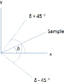
So far RAS has been considered as an optical probe of surfaces using light of near normal incidence on a stationary sample. However, if the sample is rotated in the plane of the surface, in the ‘azimuthal’ angle, a more thorough understanding of the surface can be obtained. This is called azimuthal dependent reflection anisotropy spectroscopy (ADRAS). For example, ADRAS can gain information on the optical anisotropy of adsorbed species on a surface [7,15,16,17] but also understand how clean surfaces behave as they are rotated.


![Figure 3.11: Schematic diagram of the electrochemical cell from [29]. a) top view and b) cross](https://thumb-us.123doks.com/thumbv2/123dok_us/8062059.226153/64.595.247.424.70.342/figure-schematic-diagram-electrochemical-cell-view-b-cross.webp)
![Figure 4.2: Interband absorption spectrum at 300 K [7].](https://thumb-us.123doks.com/thumbv2/123dok_us/8062059.226153/78.595.234.400.317.512/figure-interband-absorption-spectrum-at-k.webp)

