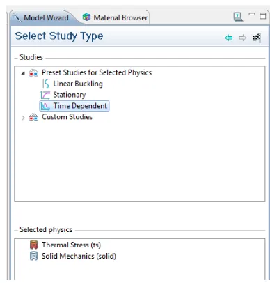
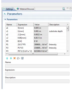
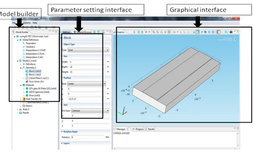
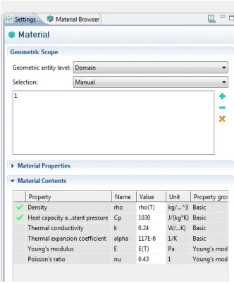
0. Introduction
Department Of Engineering
PhD Thesis
A Predictive Thermal Dynamic Model for
Parameter Generation in the Laser Assisted
Direct Write Process
Thesis submitted in accordance with the requirements of the University of Liverpool for the degree of Doctor in Philosophy
By
Shuo Shang
0. Introduction
Declaration
I hereby declare that this submission is my own work and that, to the best of my knowledge and belief, it contains no material previously published or written by another person nor material which to a substantial extent has been accepted for the award of any other degree or diploma of the University or other institute of higher learning, except where due
acknowledgment has been made in the text:
0. Introduction
Abstract
The Laser Assisted Direct Write (LADW) method can be used to generate electrical circuitry
on a substrate by depositing metallic ink and curing the ink thermally by a laser. Laser curing
has emerged over recent years as a novel yet efficient alternative to oven curing. This method
can be used in-situ, over complicated 3D contours of large parts (eg. aircraft wings) and
selectively cure over heat sensitive substrates, with little or no thermal damage.
In previous studies, empirical methods have been used to generate processing windows for
this technique, relating to the several interdependent processing parameters on which the
curing quality and efficiency strongly depend. Incorrect parameters can result a track that is
cured in some areas and uncured in others, or in damaged substrates. This thesis addresses the
strong need for a quantitative model which can systematically output the processing
conditions for a given combination of ink, substrate and laser source; transforming the
LADW technique from a purely empirical approach, to a simple, repeatable, mathematically
sound, efficient and predictable process.
This thesis describes in detail a novel and generic Finite Element Method (FEM) model that
for the first time predicts the evolution of the thermal profile of the ink track during laser
curing and thus generates a parametric map which indicates the most suitable combination of
parameters for process optimisation. Experimental data is compared with simulation results to
verify the accuracy of the model.
This study also theoretically and experimentally investigates the curing process under
different intensity profiles obtained with the SunShaper, a novel beam shaping device
invented by Dr Wellburn, and thus predicts the performance of curing with various circular
shaped beams.
0. Introduction
Acknowledgements
The Author would like to express gratitude to the following people for assistance during the
course of completing this thesis:
To my PhD supervisors Professor Ken Watkins and Dr Geoff Dearden for the numerous
helpful discussions, constructive criticism, guidance and enthusiasm which made the
experience successful and enjoyable.
To Dr Eamonn Fearon for suggestions and ideas which had a major effect on the direction of
the work presented in this thesis. To Dr Dan Wellburn, who invented the SunShaper beam
shaping device, for his assistance and support. To Dr Taku Sato whose previous study
inspired a lot of work presented in this thesis.
To all the staff at Lairdside Laser Engineering Centre particularly Dr Stuart Edwardson and
Doug Eckford for practical help of all kinds.
To Dr Robin Pittson and Dr Nina Biddle at Gwent Electronics group(GEM)for providing the inks that are used in this study.
To Dr Andrew Fogg for his assistance on utilising the STA instruments in the Department of
Chemistry, University of Liverpool.
0. Introduction
List of Publications to Date
The Author has published the following two academic papers to date, in:
Journal of Physics D: Applied Physics
A predictive thermal dynamic model for parameter generation in the laser assisted direct write process
Shuo Shang, Eamonn Fearon, Dan Wellburn, Taku Sato, Stuart Edwardson, G Dearden and K G Watkins
2011 J. Phys. D: Appl. Phys. 44 435301
(http://iopscience.iop.org/0022-3727/44/43/435301)
Optics and Lasers in Engineering
Laser Assisted Direct Write Process with Novel Beam Profiles
Shuo Shang, Eamonn Fearon, Dan Wellburn, Shilian Yan, Stuart Edwardson, G Dearden and K G Watkins
0. Introduction
Symbols and Notations
I [Wm-2], laser intensity
I0 [Wm-2], the peak intensity at the centre of a Gaussian laser beam
Ω [m], is the beam waist
r [m], is the distance away from the centre of the beam
P [W], is the power of laser
ΔQ [J], the total energy required to cure unit volume of ink from room temperature
ΔQi [J], energy required for a particular stage in a curing process
ρs [kgm-3], solvent density
Ma, the molar mass of ethanol
NA, the Avogadro constant.
Cp [Jkg-1 K-1], is the heat capacity
k [W·m−1·K−1], thermal conductivity
T [K], local temperature on the sample
σ [5.670373(21)×10−8 W m−2 K−4], the Stefan-Boltzmann constant
ϵ is the emissivity
V [m3], unit volume on the sample
In [106 Wm-3], normalised Intensity of laser , defined as the average laser intensity per micron
H [m], thickness of the ink track
R [m], half track width
Pe, Peclet number
0. Introduction
Tc [K], curing temperature
Tov [K], the overcuring temperature
kD1, kC, kD58 and kAg, [Wm-1K-1], the thermal conductivity ofcured D1 ink, pure graphite,
cured D58 ink and silver, respectively
Hi, [Wm-2], total heat flux
t [S], time of the process,
ΔT [K], temperature increment
0. Introduction
List of Abbreviations
DW: Direct Write
LADW: Laser Assisted Direct Write
FEM: Finite element Method
STA: Scanning Thermal Analysis
TGA: Thermo Gravimetric Analysis
DSC: Differential Scanning Calorimetry
PLD: Pulsed Laser Deposition
MAPLE: Matrix Assisted Pulsed Laser Evaporation
FIB: Focused Ion Beam
LIFT: Laser Induced Forward Transfer
SLS: Selective Laser Sintering
RLC: Resistance-Inductance-Capacity
CNC: Computer Numerically Controlled
PET: Polyethylene Terephthalate
0. Introduction
Table of
Content
0. Introduction --- -16
1. Literature review
--- 191.1 Overview of Direct Write technology and the purpose of this study
--- 191.1.1 DW technologies and their applications --- 19
1.1.1.1 Applications of DW technology and need for research in this area ---19
1.1.1.2 Non-laser based DW technologies ---20
1.1.1.2.1 Syringe or nozzle based technologies ---20
1.1.1.2.2 Inkjet technology --- 21
1.1.1.2.3 Screen printing --- 23
1.1.1.2.4 Photolithography --- 23
1.1.1.2.5 Thermal spray, Cold gas deposition and Sol-gel --- 25
1.1.1.3 Lasers and their applications --- 26
1.1.1.3.1 CO2 Lasers --- 26
1.1.1.3.2 Excimer Lasers --- 27
1.1.1.3.3 Solid State Lasers --- 28
1.1.1.3.4 Ultrafast Lasers --- 28
1.1.1.3.5 Applications of laser technology --- 29
1.1.1.4 Laser based DW --- 29
1.1.1.4.1 Laser micromachining --- 29
1.1.1.4.2 Pulsed laser deposition (PLD and MAPLE) --- 30
0. Introduction
1.1.1.4.4 Selective laser sintering (SLS) --- 32
1.1.2 Laser assisted direct write (LADW) --- 34
1.1.2.1 Review of the LADW process --- 34
1.1.2.2 Applications of LADW technology --- 35
1.1.2.3 Inks and materials used for LADW --- 36
1.1.2.4 Beam shaping technologies and their applications --- 37
1.1.2.5 Curing mechanisms of polymer inks --- 38
1.1.2.6 Mathematical modelling of Laser material processing --- 40
1.1.3 Summary --- 41
1.2 Overview of the Finite Element Method and its application in this study
--- 421.2.1. Introduction of the Finite Element Method (FEM) --- 42
1.2.2 Background on numerical methods --- 42
1.2.3 Outline of FEM methodology --- 43
1.2.4 FEM modelling for laser surface heat treatment --- 44
2. Theoretical background and model construction
--- 452.1 Curing process overview
--- 452.2 Schematics of configuration
--- 452.3 Materials
--- 462.3.1 Inks --- 46
0. Introduction
2.4 Laser intensity distributions
---482.4.1 Gaussian --- 48
2.4.2 Top-hat --- 48
2.4.3 Annular filled ring ---49
2.4.4 Power integration over the beam focal spot --- 50
2.5 Curing mechanism
--- 502.5.1 Coupled laser energy --- 51
2.5.2 Effective Specific Heat Capacity --- 52
2.5.3 Absorption coefficient --- 53
2.5.4 Thermal conductivity --- 54
2.5.5 Governing conductive heat equation --- 56
2.5.6 Boundary conditions --- 56
2.5.7 Curing criteria --- 57
2.5.8 Assumptions --- 59
2.6 Model building
--- 592.6.1 Overview --- 59
2.6.1.1 General model strategy --- 59
2.6.1.2 Comsol Multiphysics environment --- 60
2.6.1.3 Hardware requirement --- 61
2.6.2 Model construction --- 62
2.6.2.1 Initiating model type and select of physics involved --- 62
0. Introduction
2.6.2.3 Application of material physics and boundary conditions --- 66
2.6.2.4 Meshing --- 68
2.6.3 Interpretation of result --- 69
3. Experimental method --- 72
3.1 Introduction
--- 723.2 Equipment
--- 723.2.1 Synrad laser marking system --- 72
3.2.2 Fluid dispensing equipment --- 74
3.2.3 The SunShaper --- 78
3.2.4 The Solsurf laser processing system --- 80
3.2.5 The beam intensity attenuator --- 82
3.2.6 The LaserDec beam analyser --- 83
3.2.7 The Elcometer pencil hardness tester --- 85
3.2.8 The Digimess RLC meter --- 86
3.3 Materials
--- 873.3.1 Inks --- 87
3.3.1.1 Ink properties --- 87
3.3.1.2 Principles of DSC, TGA and DTA --- 90
3.3.1.3 Perkin Elmer STA 6000 System --- 91
3.3.2 Substrates --- 94
3.4 Experimental procedure
--- 950. Introduction
3.4.1.1 Dr Blade method --- 95
3.4.1.2 CNC deposition with the dispensing robot --- 97
3.4.2 The laser curing method --- 99
3.4.2.1 Defocused curing with the Synrad laser system --- 99
3.4.2.2 Curing with the shaped beam profiles on the Solsurf system --- 100
4. Results, analysis and discussion
--- 1014.1 Simulation of generic ink tracks on PET substrates with Gaussian beam
--- 1014.1.1 Simulation results --- 101
4.1.2 Linear temporal analysis --- 104
4.2 Curing of D58 ink tracks on various substrates
--- 1074.2.1 Parametric curing map --- 107
4.3 Curing D58 ink tracks with shaped beam profiles
--- 1144.3.1 Shaped beams obtained with the SunShaper --- 115
4.3.2 The Peclet Number and its relevance to this work --- 116
4.3.3 Temperature disparity --- 118
4.3.4 Resistivity and hardness test result --- 122
4.4 LADW process with Carbon based D1 ink ---
1244.4.1 Direct results of STA analysis --- 124
4.4.2. Weight loss and heat flow analysis --- 126
0. Introduction
4.4.4 Simulation and experimental results --- 133
4.4.5 Variations in processing conditions and parameters --- 135
5. Conclusions and future work --- 136
5.1 Conclusion
--- 1365.1.1 Summary of works presented in this study --- 136
5.1.2 Conclusions of study --- 138
5.2 Future work
--- 1395.2.1 FEM Model for Multi-pass LADW processes --- 139
5.2.2 Thermal stress generated during LADW --- 140
5.2.3 Formulation of the Chemistry involved in the process --- 140
5.2.4 Validation of models by temperature monitoring --- 140
6. References --- 141
7.Appendix --- 152
7.1 Types of partial differential equations --- 152
7.2. Solving one-dimensional problem with FEM --- 152
7.2.1 Variational formulation for one dimensional problem --- 153
7.2.2 Discretisation of variational formulations --- 155
7.2.3 Obtaining a solution with Galerkin’s method --- 157
7.2.4 Error estimation for FEM --- 158
7.2.5 The Ritz method for FEM --- 159
0. Introduction
7.3.1 Poisson problems in 2D and higher dimensions --- 160
7.3.2 Local stiffness matrix and global stiffness matrix --- 164
7.4 Hilbert space and weak formulation --- 165
7.4.1 The Hilbert space --- 165
7.4.2 The weak formulation --- 166
7.4.3 Variational forms for Neumann problem --- 167
7.5 Parabolic problems --- 168
7.5.1 Classical parabolic problems --- 168
0. Introduction
0. Introduction
As technology progresses, there is a tendency and requirement for electronics to become
smaller, cheaper and more reliable. Further to this, in an energy conscious environment there
is a desire for more efficient ways of manufacturing components with less material waste and
shorter life cycles.
Direct Write (DW) process is able to fabricate components of different geometries and
materials, from tissue scaffolds for cells to ceramics and piezoelectric materials. There is
extensive growth in the area of DW research with numerous commercially available systems
already in industrial usage. With the advent and growth of DW, there is a desire within
industry for the development of these processes to be used to fabricate functional components
for real world solutions. With many technologies each with their own merit, no single
technology has become the sole solution for all fabrication needs.
Many DW processes were already well established before industrial lasers became ready.
They are generally relatively easy to operate and are suitable for large quantity batch
production. However some of such methods lack flexibility, therefore are unsuitable for
prototyping or low volume manufacture. Also, the usage of volatile chemicals involved in
some cases has strong negative environmental impacts.
A laser has the ability to direct variable amounts of energy precisely to where it is needed in a
controllable way. Different types of lasers have been developed with new types constantly
being introduced. Applications of lasers have been found in countless fields.
The Laser Assisted Direct Write (LADW) process is an additive deposition process which
uses laser energy to thermally cure a pre-deposited conductive ink track pattern on a substrate.
As a potential substitution to photolithography, LADW technology has received attention in
recent years for its wide range of applicability in modern electronics. LADW allows printing
of various patterns without employing a mask or a resist. Deposition speed is enhanced with
CNC integration. LADW has some advantages over conventional ink-jet methods, in that it is
able to use higher viscosity liquids containing various sizes of micro particles. In a typical
LADW process, ink is precisely deposited onto a substrate; the sample is then cured either in
an oven, or by laser irradiation along the ink track. The potential uses of this technology
0. Introduction
electronics, Organic Light Emitting Diodes (OLED) displays, antenna, biological uses and
many more.
However, there are a number of barriers to be overcome before Laser Assisted Direct Write
can be fully implemented in the commercial arena:
1) Manufacture of conductive inks which are optimised for laser curing.
2) Reliably achieving efficient laser curing with satisfactory conductivity, and
acceptable adhesion to the substrates.
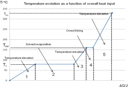
One key technical aspect of LADW is the conductive ink used. A conductive ink is typically
a fluid loaded with metallic (eg, silver) micro particles that have been fully suspended in resin.
Solvent is added to reduce viscosity for printing. Once deposited, the solvent is evaporated by
heating to leave a thin film of micro particles in resin. The composite is then further heated to
a higher temperature at which the resin starts to cross-link, and hence reduce in volume. The
silver particles are then closely packed together, yielding electrical conductivity.
Traditionally, ovens are used to cure the deposited ink.
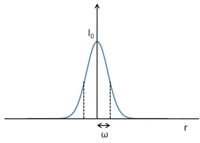
Another key factor of LADW is the mode of laser beam. A Gaussian beam intensity profile
has been most commonly used for LADW. However, a Gaussian intensity distribution is not
capable of providing uniform surface heat treatment desired by many laser processes, due to
the large disparity between the intensity at the centre of the Gaussian beam and that at its
outside edge.
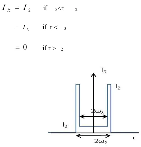
The Novel beam shaping device designed by Wellburn is a dynamic possessing head capable
of tuning the output intensity profile and/or beam geometry, with virtually no loss of input
power. It converts a CO2 laser beam of the Gaussian mode into a plateau filled annular ring
shape, the relative level of plateau fill can be easily varied by calibrated manual adjustment of
the device. The flexible beam profiles produced by the beam shaper enable study of process
optimisation for a wide range of laser surface heat treatments.
Remarkable advances have been made regarding the manufacture of inks while much less
study has been done on the development of a non-oven method of curing.
This study focuses on the construction of a predictive Finite Element Method (FEM) model
for LADW in the COMSOL 4.0 environment. This model is proposed for efficient simulation
of the curing process for different substrate/ink combinations, taking into account the
0. Introduction
which will be useful as a guide to engineers for the optimisation of the process. Close
approximation is made to generate an indicative parametric map which is validated with
experimental results.
This model simulates the temperature evolution of the sample during the process. The results
can be used to predict whether satisfactory curing has been achieved and thus indicate the
suitability of the combination of curing parameters used. Laser intensity profiles can be
defined in the model as analytical functions, or imported as interpolation functions, and one
can therefore predict the optimised beam mode by running the model.
Experimental validations of simulation results have been performed in this study, along with
1. Literature review
1. Literature review
This chapter presents a literature review for the topic of study. The first part is intended to
inform the reader of the current state of the art of technology used under the umbrella term
“Direct Write”, focusing on the LADW technology. This is followed by the second part
which briefly introduces the background of Finite Element Method for mathematical
modelling, which is a critical part of this thesis.
1.1 Overview of Direct Write technology and the purpose of this study
Additive manufacturing, for which Direct Write (DW) is a sub-category, is a well suited
manufacturing tool. In general it allows for low material wastage and ease of modification.
Due to its computer controlled nature, different designs can be easily made with just a change
in programming and no requirement for hard tooling [1-8]. With no single dominant process,
it is likely that several will emerge as the process of choice for any single component
manufacturing process [10-17].
This overview is split into two sections. The first section broadly introduces commonly used
“non-laser based” and “laser based” DW techniques. The second section focuses on Laser
Assisted Direct Write and previous work that has been done in this particular field.
1.1.1 DW Technologies and their applications
This chapter firstly discusses the applications and potential of DW, starting with non-laser
based additive manufacturing technologies and followed by principle of lasers and laser
based DW technologies.
1.1.1.1 Applications of DW technology and need for research in this area
The term direct write (DW) is a general umbrella term for a range of flexible multi-scale,
CAD/CAM controlled fabrication technologies which largely involve ‘point of process’
deposition and which can be used to produce 2D and/or 3D structures on pre-existing
substrates for a wide range of materials [22-25]. They can be used to form simple 2D
components or complex 3D architectures on curved surfaces.
1. Literature review
made to restrict the scope of this review to the generation of electrically significant
components on 3D substrates with no damage to the substrate. For example, sensors or
electrical components in metallic parts [13, 16, 26-35]. Some technologies are included
which may be of use in relatively large scale deposition of a desired set of materials, though
these may require some finishing processes. These are included due to the higher deposition
rates which may be useful in conjunction with the more accurate systems and for
completeness.
1.1.1.2 Non-laser based DW technologies
Many DW processes were already well established before industrial lasers became ready in
the 1980s. These methods all involve flow and chemical processes in some way. They are
generally relatively easy to operate (do not require staff to be trained in the laser optics), and
are suitable for large quantity batch production.
1.1.1.2.1 Syringe based technologies
The advantage of syringe deposition is the ability to conformally deposit a desired ink over a
surface and its capability of coping with a wide range of viscosity. Flow-based DW requires
high precision micro-dispensing technology which could be in the form of a precise
pneumatic pump or an extrusion process. A precision instrument that enables deposition of
liquid droplets spanning from 2 nano litre to 300 micro litre has been developed utilizing
piezoelectric actuators for volume control [36-40]. The material delivered is through a very
small orifice of a needle, restricting the size of the particles that can populate a composite ink.
In practice, for syringe deposition the particles are of the order tens of microns as a maximum
and recently common inks often employ nano particulates. This kind of DW system is able to
cope with materials over a wide range of viscosity from 0.5 to 1,000,000 cp. Unlike inkjet
process, where the ink is discretised as individual droplets, the delivery of material for
1. Literature review
Common components that are fabricated using this type of technology include conductive
lines, resistors, antenna and 3D polymeric structures [41], where line widths down
to 25μm have been demonstrated. Conventionally, post curing in an oven is required. This
technique is also extensively used in the biochemical field for 3D tissue engineering with
cells.
1.1.1.2.2 Inkjet technology
Inkjet technologies for the deposition of sensors have evolved from printing technologies and
can create multilayer systems by the deposition of inks containing colloids, nanoparticles,
organometallics or organic compounds (including viable cells) [42-47]. Inkjet technologies
can be separated into two broad classes based on how the ink is delivered, whether it is
delivered in a continuous stream (filamentary approach) or in a series of discrete droplets (the
more common technique) [48]. One of the most important considerations is the properties of
the ink itself, which must have the required viscosity, shear stress and viscoelasticity for the
relevant process – especially in the case of self-supporting structures. An extra consideration
when printing on hard (i.e. non-absorbent) surfaces is that the drying of the ink relies entirely
on solvent evaporation. However, the emergence of UV-curable inks has obviated this
problem to a certain extent [49-54].
Discrete droplet systems rely upon low-dilution (<5% solids by volume), low-viscosity inks
(typically 2cp but can be up to 100cp) which will form consistent droplet sizes [54]. A feature
of these low-viscosity inks is their propensity to spread on contact with the substrate, forming
tracks with a very low ratio of height to width. Filamentary systems can utilise inks with
1. Literature review
much higher concentrations of solute and higher viscoelastic properties, allowing the
generation of high-aspect ratio 3-D structures. This is because they do not require the
formation of a drop to occur which is dependent on the surface tension and viscosity of the
fluid, and so can tolerate a larger range of ink properties compared to drop on demand. Drop
on demand has very specific property requirements as the viscoelastic nature of the fluid
determines the snap off of the ligament that is formed during drop formation. This ligament
needs to break away from the droplet and re-coalesce in to the nozzle so that satellite droplets
are not formed [55-57].
Metallic paths can be printed by using a metal precursor which can be subsequently
treated to convert it to the pure metal. Silver and copper electrodes have been printed
using this technique. Ceramics can also be inkjet printed, either directly with particles in
solution (to be subsequently sintered) or by printing a binder on pre-placed ceramic particles.
The latter method is more commonly used to make ceramic moulds for casting.
In general for the fabrication of electrical components, the inkjet heads use a piezoelectric
orifice that squeezes or jets the ink out. A discrete droplet is formed in this manner.
Another technique is to thermally heat the ink (no piezoelectric orifice) creating a bubble at
the end. This bubble then bursts in a controlled manner and is directed towards the
substrate. Thermal ink jet printing has been superseded by piezoelectric ink jets due to the
inability of thermal inkjet heads to deposit volatile solvents, placing limitations upon the
[image:22.612.141.437.332.534.2]types of materials that can be deposited [34-36, 58, 59].
1. Literature review
In general, inkjet printing can create very high aspect ratio lines, with drop sizes on the
substrate about 80μm across with a 30μm diameter orifice and tens of nanometres thick.
Several overlaps are required to create a solid line. Another benefit of inkjet printing is the
use of multiple heads on any single system to increase deposition rates with hundreds of
nozzles jetting at any one time. Inkjet printing is generally limited to flat substrates, or
features of 2D patterning on 3D cylindrical substrates due to the nature of the inkjet head.
1.1.1.2.3 Screen printing
Screen printing of films with required electrical properties is an outgrowth of the printing
techniques used commercially for cloth and paper. The basic process is to use a mesh
screen, parts of which are treated to make it impermeable to an ink. This screen is then placed
over the part to be printed and ink drawn across it. The ink passes through the permeable
parts of the screen and is thus deposited on the substrate. This method has been in use to
produce thick conductive films and circuits since the 1960’s [60].
Today, the use of conductive inks and colloidal suspensions allows the deposition of
electrical components including piezoelectric ceramics [33], metals, semiconductors [61] and
the generation of batteries [62]. Though the thickness of screen printed layers can be
controlled to 1-2 microns, the width of deposited features is only accurate to a
resolution of approx 100 microns and may need to be post-processed by laser machining or
photoresist methods.
Screen printing is a very fast way of producing large batches of similar items on flat thin
substrates. It is limited by the mesh that is used and any new design requires a new mesh
to be fabricated, making it unsuitable for small batch runs. The component once deposited
will also require some form of post treatment to functionalise the ink that was deposited. It
is also a wasteful process in that the whole mesh needs to be sufficiently flooded for the
ink to permeate through it, while only a small proportion is actually used [33, 61, 63].
1.1.1.2.4 Photolithography
Photolithography is a well-established and widely applied technique for generating high
1. Literature review
· Preparation: The substrate wafer is initially heated and chemically cleaned to drive off
any moisture and remove contamination. A liquid or gaseous “adhesion promoter" is
applied to promote adhesion of the photoresist to the wafer.
· Photoresist application: The wafer is covered with photoresist by spin coating. A
viscous, liquid solution of photoresist is dispensed onto the wafer, and the wafer is
spun rapidly to produce a uniformly thick layer. The spin coating typically runs at
1200 to 4800 rpm for 30 to 60 seconds, and produces a layer between 0.5 and 2.5
micrometres thick. The spin coating process results in a uniform thin layer, usually
with uniformity of within 5 to 10 nanometres.
·
Exposure and developing: A mask is then aligned over the substrate, before exposing to uniform UV illumination [7, 64, 65]. The exposure to light causes a chemicalchange that allows some of the photoresist to be removed by a special solution, called
"developer". Positive photoresist, the most common type, becomes soluble in the
developer when exposed. With negative photoresist, unexposed regions are soluble in
the developer Fig 1.1.3 [66]. This procedure can be used to generate patterns on
variously coated surfaces with only one type of photo resist and mask.
· Etching: In etching, a liquid ("wet") or plasma ("dry") chemical agent removes the
uppermost layer of the substrate in the areas that are not protected by photoresist. In
semiconductor fabrication, dry etching techniques are generally used, as they can be
made anisotropic.
· Photo resist removal: After a photoresist is no longer needed, it must be removed
from the substrate. This usually requires a liquid "resist stripper", which chemically
alters the resist so that it no longer adheres to the substrate. Alternatively, photoresist
may be removed by a plasma containing oxygen, which oxidizes it. This process is
called ashing, and resembles dry etching.
Photolithography has been a crucial factor in the continued advance of Moore’s Law,
enabling minimum features sizes in chip manufacturing to shrink from 0.5 micrometer in
1990 to 45 nanometers and below in 2010. This trend is expected to continue into this decade
1. Literature review
1.1.1.2.5 Thermal spray, Cold gas deposition and Sol-gel
Thermal spray is a process which melts wire, rod or powder feedstock using a flame or
plasma arc to produce molten droplets which are then accelerated onto a substrate to
form a coating. It has been demonstrated to be capable of producing resolutions on the order
of 100 microns [67, 68]. It can be used to deposit metallic, polymeric or ceramic materials.
Using this technology researchers have built humidity sensors [67], strain gauges,
thermocouples and thermistors on both flat and curved surfaces [12]. This technology can be
used on a wide variety of surfaces and has low heat input into the substrate. It can be fully
automated and used in conjunction with robotics, increasing the areas in which it can be used,
also meaning that it is suitable for small batch quantities and rapid prototyping [12, 69-71].
1. Literature review
Cold gas deposition is an emerging technology whereby particles are accelerated within a
supersonic gas stream (typically helium) to impact upon a substrate. Upon impact, their
high kinetic energy results in deformation of the particle and bonding with the substrate.
This process has been demonstrated for ductile materials including aluminium [72] and
other metals [73]. It has the potential to deposit metallic paths on substrates with no heat
input and therefore no associated thermal damage to the substrate. Cold gas deposition
concentrated upon high deposition rates rather than fine accuracy. The process may produce
residual stresses within the deposited material but has oxygen concentrations similar to that
of the original powder. Due to the fact that it is not a melting process, reactions between
dissimilar materials do not occur and mixed powders can be sprayed to undergo controlled
reaction later by heating processes[72-74]. It is not apparent in the literature whether it has
been possible to produce the thin films required as a prerequisite of thin film sensor
generation.
The sol-gel process used for making ceramic and glass materials involvs a change from a
typically colloidal liquid solution "sol" to a solid "gel" phase. Using this method, it is
possible to make ultra-fine or spherical shaped powders, thin film coatings, ceramic fibers or
microporous inorganic membranes [75-78]. Inorganic or organic metal compounds are firstly
made into a colloidal solution which is then spread over a surface to produce thin films or put
into a mould to form a gel.
Drying or evaporation then results in a dense ceramic in the required form. Altering the
viscosity of a "sol" allows ceramic fibers to be drawn from It [79]. Thin film sensors of
interest that have been produced in this manner include chemical and biosensors, strain
sensors, actuators [71, 80-82] and moisture sensors.
1.1.1.3 Lasers and their applications
A laser has the ability to direct variable amounts of energy precisely to where it is needed in a
controllable way. Many different types have been developed with new types constantly being
introduced. The most common types are CO2 lasers, solid state lasers, fibre lasers, ultrafast
lasers, and excimer lasers.
1.1.1.3.1 CO2 Lasers
1. Literature review
range from several kilowatts (carbon dioxide lasers) to milliwatts (helium–neon lasers). They
can be operated in either the continuous mode or pulsed mode, with output frequency ranging
from ultraviolet to infrared. As the name implies, gas lasers use a gas as the active medium.
Common examples are the He-Ne and CO2 lasers. Electrical pumping is the most common
means of exciting the active medium in gas lasers.
The active medium for the CO2 laser is a mixture of CO2, N2, and He. The CO2
molecule provides the transitions that generate the laser beam. N2 helps to increase
the population of the upper lasing level, while He helps to depopulate the lower
lasing level, thereby enhancing the achievement of population inversion. Since N2 is
a diatomic molecule, it has only one vibrational mode, unlike the CO2 molecule. Most CO2
lasers fall into one of the following categories.
Axial Flow Lasers: In a typical axial (longitudinal) flow CO2 laser, gas mixture is made to
flow continuously through the tube along the axis [83].
Transverse flow lasers: In transverse flow lasers, the gas flow, electrical discharge or current
flow, and resonator axis are mutually perpendicular to one another. This is because the heat
generated within the discharge tube can be more efficiently extracted by flowing the gas at a
rate of about 60m/s in a direction normal to the resonator axis. This results in a reduced
operating temperature, and under such circumstances, the laser can be operated at higher
pressures.
Slab lasers: Slab lasers can have either solid-state or gas-active media [84]. Here, the active
medium is excited using two parallel rf-electrodes, which are water cooled. The system is
thus said to be diffusion cooled. As a result, the conventional gas circulation systems
involving roots blowers or turbines are not required. The use of slab geometry for the active
medium enables the beam quality to be significantly improved.
1.1.1.3.2 Excimer Lasers
Excimer lasers are another kind of common gas laser based on the transition of an excited
diatomic molecule to a lower energy state where it dissociates into single atoms. The
potential energy of a diatomic molecule (dimer) depends on the separation distance between
the nuclei centres of the individual atoms [76, 85].
Excimer lasers are useful in applications where ultraviolet output is required. XeCl excimer
lasers have been used in laser-assisted chemical vapour deposition for semiconductor
manufacture, also photochemical reactions, and photo ablation of polymers, ceramics and
1. Literature review
1.1.1.3.3 Solid State lasers
Solid-state lasers normally use an insulating crystal or glass as the host lattice. In it is
embedded the active medium, which is either a dopant or an impurity in the host material.
The crystal host material does not participate directly in the lasing action, while the dopant
does. It is normally a transition metal or rare earth element, and it substitutes for some of the
atoms in the host material. The active medium is shaped in the form of a rod, a slab or a disk.
Pumping is commonly done using a flash lamp or a diode [86-91].
The active medium temperature may be controlled by circulating air or liquid around it.
Otherwise, the heat generated can change the cavity dimensions and consequently, the cavity
modes.
Most solid-state lasers generate pulsed beams, even though some generate continuous
wave outputs. Common types of solid-state lasers include the ruby, Nd:YAG and Nd:Glass
lasers.
The most recent and significant development in laser technology is the advent of the fibre
laser, where the fibre is used as the cavity producing high quality high power beams with the
ease of a fibre optic for integration.
Advantages of fibre lasers include the following [92]:
1. Compact design, since the fibers can be packaged in a coiled configuration. In fact the
term “briefcase laser” has been used to refer to these types of lasers.
2. High beam quality (diffraction limited) that results from the use of single-mode fiber
cores.
3. Relatively high output efficiency of about 50 % compared to about 10–30 % for CO2 and
2 % for lamp pumped Nd:YAG lasers.
1.1.1.3.4 Ultrafast Lasers
The laser systems discussed thus far are capable of generating either continuous wave or
pulsed beams with pulse duration of up to hundreds of nanosecond duration by either
Q-switching or mode-locking. Shorter laser pulses of duration down to picoseconds and
femtoseconds are obtained with ultrafast lasers [93, 94]. These enable much higher peak
intensity to be obtained. The output wavelength can be varied with built-in optical crystals.
Regardless of the low maximum power (~50W) [93], the high peak intensity and repetition
1. Literature review
1.1.1.3.5 Applications of laser technology
Over the past five decades, applications of lasers have been found in countless fields, from
medical treatment, to car manufacture; from commercial display to defence related
technologies. A laser can be used for welding, cutting, drilling, marking, engraving, and
cleaning. In this study, the scope to laser material interaction is limited to creating surface
structures.
Applications rely on the coherent and monochromatic nature of a laser. Lasers can be used to
create small features on a suitable substrate by using additive, ablative or reactive chemical
methods. For fine (<100 micron) features, the shorter wavelength lasers are most commonly
used. These include Excimer (193 and 248nm wavelength), frequency doubled or frequency
tripled Nd:YAG and high beam quality short-pulse lasers (nanosecond pulsed or lower). With
additive processes, lasers can be used to generate 2D and 3D structures at resolutions of tens
of microns, whereas laser machining or ablative processes can remove pre-placed materials in
defined patterns to a feature resolution of less than half a micron. With some processes, laser
machining is used as a final step to remove unwanted material which has been deposited in
order to refine the deposited feature to the required dimensions [22, 24, 25, 95-104].
1.1.1.4 Laser based DW
Laser technologies make many new direct write processes possible and economical. A laser
could be used to remove unwanted material on a coating through ablation or could be used to
create a coating; or to induce chemical reactions within the pre-laid surface ink structure.
These applications generally involve state of the art laser systems and deposition facilities.
And trained expertise is required to operate such machines. However for many applications
there may not be any valid alternatives.
1.1.1.4.1 Laser ablation
A short pulse laser of the order of femtoseconds or picoseconds can be used in a process that
is termed ablation or spallation depending on the exact mechanism involved. A constant
stream of pulses of a specific wavelength and frequency are incidented upon the material to
be removed/deposited, the high peak energy strips off the electrons of the material under
irradiation, the remaining positively charged lattice than expels and explodes [68, 71, 105,
106]. This process allows efficient small area precision machining on almost any surface with
virtually no heat affected zones, hence also referred to as “cold machining” [94, 107-109].
1. Literature review
pattern on a coated thin film. The number of applications of this technique is expected to
increase considerably in the coming years due to the availability of higher average power
lasers and decreasing cost. The throughput of such process can also be potentially improved
with new techniques such as beam splitting with the spatial light modulator [94, 107].
1.1.1.4.2 Pulsed laser deposition (PLD and MAPLE)
PLD is a process that uses an off axis pulsed laser to vaporise areas of a sacrificial rotating
target such that the resultant plume of evaporated material is deposited upon a facing
preplaced substrate. PLD has usually been used to deposit ceramics [110] and
semiconductors [111]. It is not suitable for depositing organic or polymeric materials due to
the high temperatures and violent mechanism of deposition. Typically it employs UV lasers
(usually excimer) and takes place within a hard vacuum, as shown in Fig 1.1.5. PLD is used
almost exclusively for the generation of thin films with area coverage, and as a result any
component desired would need to be fabricated by post laser-machining or etching of some
sort in order to be of use as a functional component. In addition the need for a vacuum
chamber would raise problems for the generation of components and would not be suitable
for 3D conformal deposition.
PLD is a popular technique where thin films are required. T. Miller et al [106] describe the
fabrication of micro-scale ITO (Indium Tin Oxide) thin film strain sensors using a
combination of PLD and focussed ion beam (FIB) machining [19, 106, 110-112].
MAPLE stands for Matrix Assisted Pulsed Laser Evaporation (MAPLE), and is a hybrid
technique of PLD for the soft deposition of polymers and organic material, but is not suitable
for the deposition of biological materials as they must be frozen within a Matrix [113-115].
1. Literature review
In this technique an ultraviolet (excimer) laser pulse is directed at a sacrificial target which
consists of a dilute matrix of a specifically chosen solvent and the organic material (solute) to
be deposited. The solvent is chosen so that it has a near zero sticking coefficient on the
substrate and preferentially absorbs the laser radiation over the organic molecules to be
deposited. The matrix is frozen along with the target being rotated in order to reduce the
effects of localised heating by successive laser pulses striking the same area and hence
reducing the effect of decomposition of the organic molecules.
When the laser beam irradiates the target, the solvent is evaporated, imparting kinetic energy
to the released polymer molecules. This effect appears as a plume being ejected from the
frozen target. If a substrate is placed in the path of this plume it will be coated with a thin
layer of polymer molecules. The gaseous solvent is evacuated from the chamber by means of
a pump [19, 113-120].
In order to create any functional geometric components, post processing of the thin film
would be required as with PLD. This could be done using a laser or some other subtractive
technique. The benefit of MAPLE over PLD is its ability to deposit organic and piezoelectric
material without any adverse side effects.
1.1.1.4.3 Laser induced forward transfer (LIFT)
LIFT is a relatively cheap and simple DW manufacturing technique that relies on a disparity
between the optical, thermo-physical and mechanical properties of the materials involved.
It has been shown to work over a range of laser wavelengths, pulsed and continuous wave
(CW). The deposition of metals, oxide compounds and diamond particles have been
demonstrated on a variety of substrates [25] in a vacuum, inert and air atmospheres, along
with the capability of fabricating precise 3D structures.
The process was first demonstrated by Bohandy et al [121] in the 1980s where it was shown
that deposition of Cu and Ag lines of ~50 μm in width could be achieved. It is a process
which uses a focussed laser to vaporise a thin film which has been placed on a laser
transparent medium which acts as a supporting plate; usually quartz but specific to the
wavelength used. The laser passes through the transparent medium and impinges upon the
film at the thin film/supporting plate interface, where it is absorbed and causes a small
portion of the film to vaporise. The vaporised material is expelled away from the
supporting plate due to the high pressures that occur during vaporisation, and recondenses
1. Literature review
Though the amount of material deposited and the achievable resolution is related to the
film thickness, laser intensity, wavelength and optical extinction coefficient of the target,
the substrate must be held in close proximity to the target so that the vaporised material
does not diverge during propagation. Typically the substrate will be between 25 μm to 100
μm from the target material [122] and this distance is directly proportional to the width of the
track deposited as well as the laser fluence employed [123].
Because LIFT causes the vaporisation of the transfer material, it is not generally
considered to be appropriate for the transfer of polymers, though they may be used as a
sacrificial binder in certain applications. It has also been demonstrated that successful
deposition of bio molecules such as DNA [124], proteins, prokaryotic and eukaryotic
cells[125] has been achieved.
1.1.1.4.4 Selective laser sintering (SLS)
Selective Laser Sintering (SLS) is an extension of the laser cladding process in that it allows
3D parts to be built by sintering successive layers on top of one another in predetermined
vector paths. The process utilises a laser beam to create a melt pool on a substrate into which
powder is incorporated and subsequently melted. A roller or scraper is used to deposit a thin
layer of powder over a piston, and then a laser is used to scan over defined areas, sintering or
fusing the powder together, as illustrated in Fig 1.1.7. The piston is then lowered and a new
layer of powder deposited to allow the generation of successive layers [126-128].
By repeating the process on top of this generated layer a 3-dimensional part can be made in a
layered manufacturing form. Since the layers are fusion bonded to each other, a fully dense
metallic part can thus be made. At present, most laser deposited parts need some post-process
machining to finish them to required tolerances [129]. The build direction has a significant
1. Literature review
effect on part quality, in terms of dimensional error and surface roughness; but no influence
on mechanical properties. Table 1.1 [130] gives examples of the commercially available “state of the art” SLS systems and their capabilities.
An advantage of this process is that overhanging structures can be built, as the unsintered
powder acts as support. Any powder capable of being melted can be used in this
process and multimode powders can be used to allow high densities to be achieved.
Electron beam deposition is fundamentally the same process but uses an electron beam
rather than a laser to create the initial melt pool. One major difference between electron
beam and laser deposition is that for electron beam the process must be carried out in
a vacuum chamber. Absence of magnetic fields is also essential.
1. Literature review
1.1.2 Laser assisted direct write (LADW)
The following part of literature review focuses on the Laser Assisted Direct Write process
and its application, which is the topic of this thesis. Key aspects of the study, including
advances in conductive inks, laser intensity distribution shaping and mathematical modelling
of the process, are also addressed.
1.1.2.1 Review of the LADW process
The LADW process referred to herein is an additive deposition process which uses laser
energy to thermally cure a pre-deposited conductive ink track pattern on a substrate. As
illustrated in Fig 1.1.8, after deposition, the sample is shifted onto a X-Y stage, a laser of a
particular power and beam modes applied over the surface of the track and thus cures the
sample.
In LADW, as with any manufacturing process, the quality of the materials used is paramount
when producing high cost, high quality components. A conductive ink is typically a fluid
loaded with metallic (eg, silver) micro particles that have been fully suspended in resin.
Solvent is added to reduce viscosity for deposition. Once deposited, the solvent is evaporated
by heating to leave a thin film of micro particles in resin. The composite is then further
heated to a higher temperature at which the resin starts to cross-link, and hence reduce in
volume. The silver particles are then closely packed together and held by the cross-linked
polymer, yielding electrical conductivity ranging from approximately 1% to 10% of bulk
1. Literature review
silver [131]. Traditionally, ovens are used to cure the deposited ink. Advantages of this
method include ease of operation and that a relatively large surface area can be cured at no
additional time compared to small areas. However, oven curing is not necessarily desirable or
possible in the case of heat sensitive substrates or many pre-existing geometries.
Fearon et al. studied the laser curing process extensively using empirical methods. They
found, with single path curing under a stable laser source, for a fixed geometry of a particular
kind of ink, the range of traverse speed resulting a satisfactory cure was fundamentally
related to the thermal properties of the substrate [132].
Other work done in the field of photon-induced polymerisation has tended to focus on the
microscopic physical chemistry side of mechanism, that is, for curing with a particular
wavelength for a certain type of polymer bonding. For example, Mao et al. used in-situ
Raman spectroscopy for the direct measurement of the C = C molar concentration in the
visible light curing vinyl ester resin [133]. Eduardo Jose et al. extensively studied the
influence of different curing wavelength and chemical catalysts on the degree of conversion
of resin using an argon ion laser, LED or quartz-tungsten-halogen light, with or without a
chemical catalyst [134]. Some novel mechanisms have also been discovered. Cao et al.
achieved creation of sub-50 nm features by using the direct laser writing technique based on
single-photon photoinhibited polymerization. The super-resolution feature is realized by
overlapping two laser beams of different wavelengths to enable the wavelength-controlled
activation of photoinitiating and photoinhibiting processes in the polymerization[135].
However none of the research available provides any systematic understanding of the
macroscopic relation between irradiation level and curing quality. In this sense the work
presented in this thesis is completely novel. In this research a continuous wave CO2 laser has
been employed. The process is treated as a thermal one and depends on the thermal
association of the absorption of photons by the material. In this manner a continuous wave
laser is the primary candidate with an IR output.
1.1.2.2 Applications for LADW technology
The Laser Assisted Direct Write (LADW) method can be used to generate electrical circuitry
on a substrate by depositing metallic ink and curing the ink thermally by a laser. Laser Curing
1. Literature review
can be used in-situ, over complicated 3D contours of large parts (eg. aircraft wings) and
selectively over heat sensitive substrates with little or no thermal damage.
Compared to existing DW technologies discussed previously in this chapter, the relatively
low productivity of LADW confines its applications to the low volume, high value fields of
engineering. LADW is basically a syringe based deposition method. Inkjet printing is the
most popular conventional method for micro-fabrication on a substrate. As a potential
substitution, LADW has advantages in that it is able to use higher viscosity liquids containing
various sizes of micro particles [48]. LADW also has more flexibility than photolithography
in terms of varying deposition geometry, though the resolution achieved may not be as high.
LADW has already been extensively used in the medical field. Kim et al. evaluated the shear
bond strength (SBS) of orthodontic brackets bonded to teeth using a diode-pumped solid state
(DPSS) laser of 473 nm with various light intensity and light-curing settings[136]; Shin et al.
and Mirsasaani et al, respectively, evaluated the effectiveness of a diode-pumped solid state
(DPSS) laser as a light source for light-curing dental resin composite [137, 138]; Shahbazi et
al. demonstrated the feasibility of a novel, thin film, laser-activated adhesive in sealing
penetrative corneal wounds with a view to replacing sutures in ophthalmic operations [139].
In terms of industrial utility, Akira et al. have fabricated a new type of plastic micro lens by
laser polymerization. They found, the amount of resin polymerized by exposure to laser light
(light curing) depends on the laser power and the exposure time. The shape of the lens can be
controlled by changing the conditions of laser irradiation [140].
Other potential industrial uses of this technology cover applications in solar cells [5], Radio
Frequency Identification-tags (RFID-tags) [6], flexible-electronics [7, 28, 30], Organic Light
Emitting Diodes (OLED) displays, antenna, biological uses and many more [2, 35, 141, 142].
However, there are barriers to be overcome before Laser Assisted Direct Write can be fully
implemented in the commercial arena [143]:
3) Manufacture of conductive inks which are optimised for laser curing.
4) Reliably achieving efficient laser curing with satisfactory conductivity, and
acceptable adhesion to the substrates.
1.1.2.3 Inks and materials used for LADW
Conductive ink has been commonly and extensively used for printable electronics over the
1. Literature review
come in many forms and are selected chiefly depending on the application. But the most
common types consist of three main components: conductive particle [144] (silver particle
[145], silver flake, copper [146], aluminium, carbon particles of different grain sizes or a
mixture of the listed; recent study reports of blending carbon nano-tube into conductive inks
based in a formic acid/acetone co-solvent system[147] ), Kim et al. also studied the effect on
conductivity induced by varying particle sizes[148] ; a polymer resin which acts as a binding
agent; and a solvent, which acts as carrier and controls the viscosity of ink for printing). The
deposition process is extremely versatile. Currently the most common techniques are inkjet
printing and variations of screen printing for the high throughput required in the electronics
industry [149]. Also the printing of the substrate largely determines the type of ink and
printing method used [150]. There are also a diversified sources for the post printing curing:
electrical, microwave, plasma, laser and flash lamp annealing have all been used to a certain
extent [151]. Inks of different components and different curing/sintering mechanism could
differ greatly in performance in terms of conductivity, durability and sometimes even result
in different failure mechanisms [152].
1.1.2.4 Beam shaping technologies and their applications
Gaussian beam intensity profiles have been most commonly used for laser processing, since
they occur naturally as the operating mode for many lasers. However, a Gaussian intensity
distribution is not capable of providing the uniform surface heat treatment desired by many
laser processes. This is due to the large disparity between the intensity at the centre of the
Gaussian beam and that at its outside edge. The effect of laser mode on the surface
temperature distribution was investigated by Kar and Langlais [153] and earlier by Sharp
[154]. They suggested that a shaped beam profile can improve many laser processing
applications. Previous studies have shown ingenuity in both the intensity profiles created
[155-158] and in the methods used for creating them [159-162].
For most applications a circularly symmetric intensity profile is preferred, since it will give a
consistent result in all processing directions. The most commonly used top-hat [163] shaped
intensity profile has a circular geometry with uniform intensity. The circular shape, however,
dictates that, when the heat source or laser beam is moving, points further from its axis of
movement experience reduced beam interaction time which leads to under-heating compared
1. Literature review
achieving a relatively uniform maximum temperature rise on a surface is the annular ring.
Annular rings are noted for having some success achieving more uniform heating effects both
in stationary [164] and moving beam applications [165]. There are several methods of
carrying out the transformation, all of which are based either on the principles of reflection,
refraction, diffraction or a combination of these. However most of the existing methods
achieve beam shaping at the cost of losing 50%-60% of power [166-168], also the intensity
profiles produced cannot be easily varied for different processes.
The SunShaper designed by Wellburn [18] is a dynamic beam shaper possessing the
advantage of being capable of tuning the output intensity profile and/or beam geometry to
suit different processes, with virtually no loss of input power. It converts a CO2 laser beam of
the Gaussian mode into a plateau filled annular ring shape, the relative level of plateau fill
can be easily varied by calibrated manual adjustment of the device (Fig 1.1.9). The flexible
beam profiles produced by the SunShaper enable study of process optimisation for a wide
range of laser surface heat treatments.
1.1.2.5 Curing mechanisms of polymer inks
Remarkable advances have been made regarding the manufacture of inks[46] and in
deposition techniques, while much less study has been done on the development of a
mechanism for non-oven methods of curing.
Simone et al. [9] have studied the processing conditions to achieve functional coating on
metallic substrates from thermal setting powders with a laser source. In this work,
epoxy-polyester hybrid resin was supplied in the form of coarse powder, then coated on stainless
steel 304 sheets before being cured with a CO2 laser under a range of fluence and scan speed.
She characterised the quality of this curing process with a defined adhesion index. An
empirical model of the curing mechanism was then constructed based the results collected for
1. Literature review
this adhesion index. The material used by Simone is largely different to that in this work,
however the curing apparatus and procedure are similar. This work also extended the
representation of results from an empirical approach to a self- contained numerical model.
Friis-Pedersen et al [169] studied the thermal curing process of epoxy resin, which is a
representative ingredient of typical DW ink. An epoxy resin containing diglycidyl ether,
dicyandiamide, and an accelerator (diurone) was investigated under different curing cycles.
The mathematical prediction of the degree of curing in a thermoset as a function of time and
temperature was investigated and compared to measured data. Near-infrared analysis was
used to measure the conversion of epoxy and primary amine and the production of hydroxyl.
Modulated differential scanning calorimetry was used to measure the changes in the heat
capacity during curing. The measurements revealed differences in the primary amine
conversion and hydroxyl production, and close relation to the measurements of heat capacity
were found. The characteristics found were attributed to differences in the curing
mechanisms. The mathematical model did not incorporate these differences, and this may
have led to discrepancies between the predicted and actual values of the degree of curing.
The DSC analysis used in Friis-Pedersen’s study is also implemented in this work to obtain
the actual heat capacity curve. The mathematical model used in his study is a generic
analytical formulation which does not account the actual experimental environments. This
drawback can be sufficiently compensated with a flexible and comprehensive FEM model
that describes the exact process, as presented in this work.
Lewis et al [21, 170] modelled the curing kinetics for polyamide. Khan et al [10] studied the
sintering of silver nanoparticles with a laser. There are also other research which have been
carried out to study the effect of different light sources on the curing efficiency of resin
[171-174] .
However, there are still gaps in the quantitative understanding of the dynamic laser curing
process. There is need for a mechanism that accounts for the overall integrated effect of
material properties and laser processing parameters over the curing quality in a real LADW
situation. The work presented in this thesis aims to address these issues by providing such a
mechanism, which is then accurately formulated into a repeatable and flexibly adjustable
![Figure 1.1.2: Illustration of the inkjet nozzle jetting, using drop on demand technique [50]](https://thumb-us.123doks.com/thumbv2/123dok_us/8059215.225539/22.612.141.437.332.534/figure-illustration-inkjet-nozzle-jetting-using-demand-technique.webp)