Comparison between flying capacitor and modular
multilevel inverter
G. P. Adam,Olimpo Anaya-Lara, Member, IEEE,Graeme Burt, Member, IEEE, and J. R. McDonald, Senior Member, IEEE University of Strathclyde, Electronic and Electrical Engineering Department, Royal College Building,
204 George Street, Glasgow, G1 1XW
[email protected], [email protected], [email protected], [email protected]
Abstract─ the paper describes the operational principle of flying capacitor and modular multilevel inverters. The detailed discussions of dc link capacitors voltage balancing methods for both inverters are given in order to enable fair comparison. The causes of dc link capacitors voltage imbalance in flying capacitor multilevel inverter with more than three levels are highlighted. Computer simulation is used to compare the performance of both inverters under several operating conditions.
Key words── Cascaded multilevel inverter, diode clamped inverter, flying capacitor inverter and modular inverter.
I. INTRODUCTION
ECENTLY, voltage source multilevel inverters have received much attention of researchers and industries, because they are capable of handling high voltage with minimum voltage stress on switching devices, generate output voltage with minimum harmonic content, and generate low dv/dt and have a lower common mode voltage, which result in reduced stress on motor bearing in drive applications [1]-[3]. The most common types of multilevel inverters are:
• Diode clamped multilevel inverter. • Flying capacitors multilevel inverter.
• Cascaded multilevel inverter with isolated dc source.
Diode clamped multilevel inverter is the most accepted topology in industry for medium voltage applications such as medium voltage drive systems. However, they suffer from the problem of voltage imbalance of the dc link capacitors [2]-[7]. The problem becomes more complex with increased number of levels. Cascaded multilevel inverters have been used intensively in applications where reactive power is dominant such static synchronous compensator and active power filter [7]-[11]. However, they require complex transformers at their inputs in application involve real power exchange such as medium voltage drive system and dc transmission systems [3].
As number of levels increases, flying capacitor multilevel inverters are required number of large capacitors and complex capacitors voltage balancing method and unable to operate in applications involve large amount of reactive power [3].
Recently, modular multilevel inverter topology has been reported as an alternative to conventional multilevel inverters in medium and high voltage applications [12],[13]. It is able to overcome most of difficulties of conventional multilevel inverter and provides new set of features such:
• Modular construction
• It is extendable to any number of levels and capacitors voltage balance is attainable.
• With increased number of levels, it generates high voltage with reduced voltage stress on switching device, and extremely low total harmonic distortion.
• As number of levels increases, interface transformer and output filter can be eliminated, resulting in significant reduction in cost.
• It has fault management capability and better fault ride-through capability.
Since, there are similarities between the flying capacitor and modular multilevel inverters in their structures, operational principles and pulse width modulation techniques. In addition to, both inverters are depending on phase voltage redundancies to balance dc link capacitors rather than line-to-line redundancies as in case of diode clamped. Nonetheless, modular multilevel inverters perform better than flying capacitor inverter as number of levels increases. Therefore, detail comparisons between flying capacitor and modular multilevel inverter are investigated in this paper. Several operating conditions have been considered to demonstrate the abilities of both inverters in improving system reliability and their limitations. Computer simulation has been used to confirm the validity of the results.
II. REVIEW OF FLYING CAPACITOR AND
MODULAR MULTILEVEL INVERTER A. Flying Capacitor Multilevel Inverter
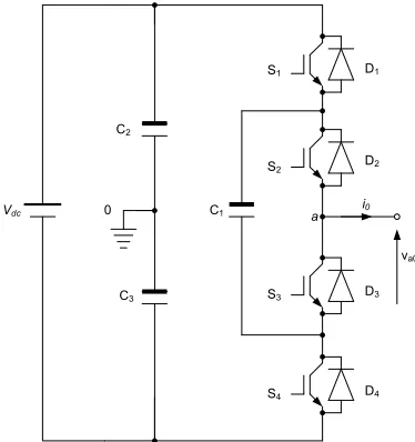
Fig. 1 shows one phase of three-phase flying capacitor multilevel inverter. Voltage across each capacitor must be maintained at ½Vdc , therefore the maximum voltage stress on switching device will be limited to one capacitor voltage [14]-[15]. The inverter in Fig. 1, produces three-level voltage between a and 0 as follow:
• For voltage level ½Vdc, switches S1 and S2 must be turned on.
• For voltage level 0, there are two possible switching combinations:
a) Switches S1 and S3 must be turned on. b) Switches S2 and S4 must be turned on.
• For voltage level -½Vdc switches S3 and S4 must be turned on.
Table 1: effect of current polarity and redundant switching states on capacitors voltage
Voltage level
Switching states
Current
polarity Current path
State of capacitors
ia>0 S1 & S2 unchanged
½Vdc 1100
ia<0 D1&D2 unchanged
ia>0 S1 &C1& D3 charges C1
1010
ia<0 S3 &C1& D1 discharges C1
ia>0 D4 &C1& S2 discharges C1
0
0101
ia<0 S4 &C1& D2 charges C1
ia>0 D3 & D4 unchanged
-½Vdc 0011
ia<0 S3 & S4 unchanged
Note: the current direction in Fig. 1 is assumed positive
From table 1 and Fig. 1, it can noticed that the voltage imbalance in three-level flying capacitor inverter can be created only when the output phase, a, is connected to 0 voltage level. The switching state 1010 charges capacitor C1
when ia>0 and discharges capacitor C1 when ia<0, while switching state 0101 discharges capacitor C1 when ia>0 and charges capacitor C1 when ia<0. Therefore, the voltage
balance of capacitor C1 can be maintained if redundant
switching states and phase current polarity are properly used. With increased number of levels the complexity capacitor voltage balancing in flying capacitor is increasing significantly due to mutual effect created by some switching states. For example, in a five-level inverter there are three groups of redundant switching states, the first group charge or discharge only one capacitor depending on load current direction; the second group affect two capacitors in each instant, they charge one of the capacitor and discharge the other depending of load current polarity. The third group of redundant switching states affect three capacitors in each instant, they charge two capacitors and discharge the remaining one capacitor or vice versa depending on load current polarity. As a result the flying capacitor multilevel inverters with more three-level are unable to operate with zero power factor (or application involve large amount of reactive power such reactive power compensation devices).
S1
S2
S3
S4
C1
C2
C3
D1
D2
D3
D4
va0
0
Vdc i0
[image:2.612.73.260.470.669.2]a
Fig. 1: One-phase of three-level flying capacitor (also known as capacitor clamped) inverter
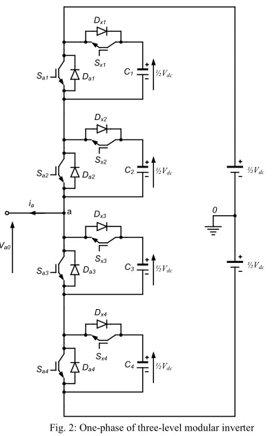
B. Modular multilevel inverter
Fig Fig. 1 shows one-phase of a three-level modular inverter. There are two groups of switches, main switches Sa1, Sa2, Sa3 and Sa4; and auxiliary switches Sx1, Sx2, Sx3 and
Sx4. There are four complementary switch pairs per phase (Sa1, Sx1), (Sa2, Sx2), (Sa3, Sx3) and (Sa4, Sx4), such that
Sai+Sxi=1, where i=1 to 4, 1 represents ON-state and 0 represents OFF-state. For example, turning on Sa1 prevents
Sx1 from being turned on.
For a three-level inverter each capacitor in the circuit must be maintained at ½Vdc; in each instant four switches
must be in ON-state, two from the main switches and the remaining two from the auxiliary switches; the voltage stress on each switching devices is limited to one capacitor voltage. Assume the supply midpoint in Fig. 2 as the output voltage reference, the three-level waveform between output phase a, and 0 can be synthesized as for follow:
• For voltage level Va0=½Vdc, turn on all the upper main switches (Sa1 and Sa2) and all lower auxiliary switches (Sx3 and Sx4).
• For voltage level Va0=0, there are four different switching combinations:
i) Turn on Sa1, Sa3, Sx2 and Sx4.
ii) Turn on Sa2, Sa3, Sx1 and Sx4.
iii)Turn on Sa2, Sa4, Sx1 and Sx3.
iv)Turn on Sa1, Sa4, Sx2 and Sx3.
• For voltage level Va0=-½Vdc, turn on all upper auxiliary switches (Sx1 and Sx2) and all lower main switches (Sa3 and
Sa4).
For an n-level modular inverter the voltage across each capacitor and switching device is limited to Vdc/(n-1). The total number of capacitors required is 6n-6 (2n-2 per phase) and the number of switches (IGBT plus free wheeling diode) is 4(n-1), which is double compared to conventional multilevel inverter.
In a three-level modular inverter the zero voltage level can be synthesized in four different ways 1010/0101, 0110/1001, 0101/1010 and 1001/0110. Consider the switching state (1010/0101) as an example and assume the current direction in Fig. 2 as positive, for ia>0 the upper capacitor C2 charges and lower capacitor C4 discharges;
while upper capacitor C2 discharges and lower capacitor C4
charges for ia<0. Table 1 summarizes all switching states and their effect on individual capacitors voltage.
From Fig. 2 and table 2, it can be concluded that for a three-level modular inverter when phase a output is attached to zero voltage level the capacitors voltages behave as follows:
• During the positive half cycle of the load current (ia>0), the upper capacitors are charging and lower capacitors discharging.
½Vdc
½Vdc
½Vdc
½Vdc
½Vdc
½Vdc 0
C1
C2
C3
C4
Sa1 Da1
Sa2
Sa3
Sa4
Da2
Da3
Da4
Sx1
Dx1
Sx2
Sx3
Sx4
Dx2
Dx3
Dx4
ia
a
[image:3.612.72.269.51.367.2]Va0
Fig. 2: One-phase of three-level modular inverter
Table 2: Effect of redundant switching states on capacitors voltages of a three-level modular converter.
Load current Switching
states Direction Path
Effect on capacitors voltages
0
a
i > Sa1Dx2 & Sx4Da3
C2
↑
and C4↓
(A) 1010
0
a
i < Sx2Da1 & Sa3Dx4
C4
↑
and C2↓
0
a
i > Sa2Dx1 & Sx4Da3
C1
↑
and C4↓
(B) 0110
0
a
i < Sx2Da1 & Sa3Dx4
C4
↑
and C1↓
0
a
i > Sa2Dx1 & Sx3Da4
C1
↑
and C3↓
(C) 0101
0
a
i < Sx1Da2 & Sa4Dx3
C3
↑
and C1↓
0
a
i > Sa1Dx2 & Sx3Da4
C2
↑
and C3↓
(D) 1001
0
a
i < Sx2Da1 & Sa4Dx3
C3
↑
and C2↓
Note: ↑represents charging state and ↓represents discharging state.
• Each capacitor cell is used only for half of the fundament period. In order to maintain voltage balance of each capacitor cell, the mean current drawn by each capacitor must be zero over one fundamental cycle. For an n-level inverter, each capacitor will be used only for 1/(n-1) of the fundamental period, therefore with increased number of levels, each capacitor will be used for a short period of time and as a result a significant reduction in capacitor size can be achieved.
• In a modular multilevel inverter, switching device utilization is independent of its location in the circuit and of the modulation.
Based these facts, the capacitor voltage balancing method for a three-level inverter is developed and summarized as follows:
1- Sort the upper and lower capacitors according to their voltages and identify capacitors with maximum and minimum voltages using the following criteria:
_ max max( 1, 2)
upper c c
K = V V , Kupper_ min=min(V Vc1, c2),
_ max max( 3, 4)
lower c c
K = V V .
2- During the positive half cycle of the load current, select a switching state that charges the upper capacitor with minimum voltage and discharges the lower capacitor with maximum voltage.
3- During the negative half cycle of the load current, select a switching state that discharges the upper capacitor with maximum voltage and charges the lower capacitor with minimum voltage.
The capacitors voltage balancing method for a modular multilevel inverter with a large number of levels is similar to that of a three-level modular inverter except that more sophisticated software overhead is needed to sort the capacitors according to their voltages in order to determine which switching state must be selected. With increased number of level the voltage balance of dc capacitors in modular inverter remain achievable with reduced complexity of the balancing method despite significant increase in number of redundant states compare to capacitor clamped inverter. The modular multilevel inverters perform better than conventional multilevel inverters because they combined the advantages of conventional multilevel inverters such as:
• Requires only one dc source and synthesizes intermediate voltage levels using dc link capacitors.
• Utilizes of phase redundancy to balance dc link capacitors regardless of number of levels, power factor and modulation index.
III. SIMULATION
In this paper, sinusoidal pulse width modulation (SPWM) with frequency of 2.1 kHz is used as the basic modulation method for both converters. The dc link voltage of 2kV and dc link capacitors each 2200µF is used with both converters. The performance of the three-level and five-level flying capacitor and modular multilevel inverters are evaluated under several scenarios to enable fair comparison. The main scenarios are:
1. Effect of load power factor on dc link capacitor voltage balance.
2. Effect of modulation on dc link capacitor voltage balance.
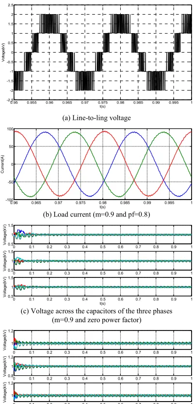
The effect of load power factor and modulation index on voltage balanced of the dc link capacitors of the three and five-level flying capacitor and modular multilevel inverters are investigated. To achieve these objectives, first three-level flying capacitor and modular converter are considered. The results in Fig. 3 and 4 are obtained with three-level flying capacitor and modular inverters. The initial voltage of capacitor C1 (Flying capacitor inverter) for the phase legs a,
inverter, the initial voltages for the capacitors of the three phases are Vc1=950V, Vc2=1050V, Vc3=1050V and Vc4=950V. It can be seen that the dc link voltage balance of flying capacitor and modular inverter are attainable regardless of load power factor and modulation index. However, with unity power factor and unity modulation index the capacitor voltages took longer to reach their set points than any other cases. The results of capacitor voltages obtained with modular inverter show some ripple in capacitor voltage. This is because, each dc capacitor in the structure has the opportunity to be charge for one fourth of fundamental and discharge for the remaining one fourth of the period as explain in section II, B.
0.95 0.955 0.96 0.965 0.97 0.975 0.98 0.985 0.99 0.995 1
-2 -1.5 -1 -0.5 0 0.5 1 1.5 2 t(s) V o lt a g e (k V )
(a) Line-to-line voltage
0.95 0.955 0.96 0.965 0.97 0.975 0.98 0.985 0.99 0.995 1
-100 -50 0 50 100 t(s) c u rr e n t( A )
(a) Load current ( m=0.9 and pf=0.8 lagging)
0 0.01 0.02 0.03 0.04 0.05 0.06 0.07 0.08 0.09 0.1
900 920 940 960 980 1000 1020 1040 1060 t(s) V o lt a g e (V )
(c) Voltage across capacitor C1 (zero power factor and m=1)
0 0.01 0.02 0.03 0.04 0.05 0.06 0.07 0.08 0.09 0.1
0.9 0.95 1 1.05 1.1 t(s) V o lt a g e (k V )
(d) Voltage across capacitor C1 (m=0.9 and pf=0.8)
0 0.01 0.02 0.03 0.04 0.05 0.06 0.07 0.08 0.09 0.1
0.9 0.95 1 1.05 1.1 t(s) V o lt a g e (k V )
[image:4.612.330.530.57.472.2](e) Voltage across capacitor C1 (m=1 and pf=1)
Fig. 3: key waveforms obtained with three-level flying capacitor inverter
0.95 0.955 0.96 0.965 0.97 0.975 0.98 0.985 0.99 0.995 1 -2.5 -2 -1.5 -1 -0.5 0 0.5 1 1.5 2 2.5 t(s) V o lt a g e (k V )
(a) Line-to-ling voltage
0.96 0.965 0.97 0.975 0.98 0.985 0.99 0.995 1
-100 -50 0 50 100 t(s) C u rr e n t( A )
(b) Load current (m=0.9 and pf=0.8)
0 0.1 0.2 0.3 0.4 0.5 0.6 0.7 0.8 0.9 1
0.5 1 1.5 V o lt a g e (k V )
0 0.1 0.2 0.3 0.4 0.5 0.6 0.7 0.8 0.9 1
0.5 1 1.5 V o lt a g e (k V )
0 0.1 0.2 0.3 0.4 0.5 0.6 0.7 0.8 0.9 1
0.5 1 1.5 t(s) V o lt a g e (k V )
(c) Voltage across the capacitors of the three phases (m=0.9 and zero power factor)
0 0.1 0.2 0.3 0.4 0.5 0.6 0.7 0.8 0.9 1
1 1.2 V o lt a g e (k V )
0 0.1 0.2 0.3 0.4 0.5 0.6 0.7 0.8 0.9 1
0.8 1 1.2 V o lt a g e (k V )
0 0.1 0.2 0.3 0.4 0.5 0.6 0.7 0.8 0.9 1
1 1.2 t(s) V o lt a g e (k V )
(d) Voltage across the capacitors of the three phases (m=0.9 and pf=0.8)
0 0.1 0.2 0.3 0.4 0.5 0.6 0.7 0.8 0.9 1
0.8 1 1.2 V o lt a g e (k V )
0 0.1 0.2 0.3 0.4 0.5 0.6 0.7 0.8 0.9 1
0.5 1 1.5 V o lt a g e (k V )
0 0.1 0.2 0.3 0.4 0.5 0.6 0.7 0.8 0.9 1
0.8 1 1.2 t(s) V o lt a g e (k V )
(e) Voltage across the capacitors of the three phases (m=1 and pf=1) Fig.4: Key waveforms obtained with three-level modular inverter
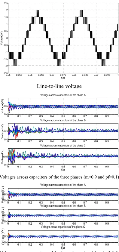
Fig. 5 and 6 show the results obtained with five-level flying capacitor and modular inverters using the same dc link voltage and capacitors used with three-level. Fig. 5 shows line-to-line voltage, load current and voltage across the capacitors of one phase. It can be seen that the capacitors voltages are diverging gradually from their set points (¼Vdc,
[image:4.612.81.285.191.652.2] [image:4.612.329.532.505.609.2]voltages are settle at the values higher than their desire set points. These may increase the voltage stress on switching devices.
2.95 2.955 2.96 2.965 2.97 2.975 2.98 2.985 2.99 2.995 3 -2.5
-2 -1.5 -1 -0.5 0 0.5 1 1.5 2 2.5
t(s)
V
o
lt
a
g
e
(k
V
)
Line-to-line voltage
2.95 2.955 2.96 2.965 2.97 2.975 2.98 2.985 2.99 2.995 3
-100 -50 0 50 100
t(s)
C
u
rr
e
n
t(
A
)
Load current (m=0.9 and pf=0.8)
0 0.5 1 1.5 2 2.5 3
0 0.5 1 1.5 2 2.5 3
t(s)
V
o
lt
a
g
e
(k
V
)
Vc1 Vc2 Vc3
Voltages across capacitors of the one phase (m=0.9 and pf=0.8)
0 0.5 1 1.5 2 2.5 3
0.4 0.6 0.8 1 1.2 1.4 1.6 1.8
t(s)
V
o
lt
a
g
e
(V
d
c
)
Vc1 Vc2 Vc3
Voltages across capacitors of one phase (m=0.9 and pf=0.1)
0 0.5 1 1.5 2 2.5 3
0.4 0.6 0.8 1 1.2 1.4 1.6 1.8 2
t(s)
V
o
lt
a
g
e
(k
V
) Vc1
Vc2 Vc3
[image:5.612.81.284.89.648.2]Voltage across capacitors of one phase (m=1 and pf=1) Fig. 5: Key waveforms obtained with five-level flying capacitor inverter
Fig. 6 shows that the modular inverters with more than three-level perform better than flying capacitor over full linear range of modulation indices and load power factors.
Since each capacitor in the modular multilevel converter circuit has the opportunity to be used for only 1
1
n− T, where T
is fundamental period; half of this period will be used to charge the capacitor and the remaining half to discharge it, according to the load current direction. For the remaining
period of 1
1
n
T− − T , the capacitor will remain unaffected as in the last state.
This feature allows capacitors voltages to vary over a limited range depending on the operating conditions and it will not allow capacitor voltage divergence under any circumstance unless the load current becomes unipolar. This situation is expected during the subtransient period when currents in some of the phases are riding over decaying dc offsets for the first few cycles following three-phase faults, and then the capacitors voltage will start to recover when the dc offset is damped. This condition will not be discussed here because it is out of scope of this paper.
0.95 0.955 0.96 0.965 0.97 0.975 0.98 0.985 0.99 0.995 1
-2.5 -2 -1.5 -1 -0.5 0 0.5 1 1.5 2 2.5
t(s)
V
o
lt
a
g
e
(k
V
)
Line-to-line voltage
0 0.1 0.2 0.3 0.4 0.5 0.6 0.7 0.8 0.9 1
0.4 0.5
Voltages across capacitors of the phase A
V
o
lt
a
g
e
(k
V
)
0 0.1 0.2 0.3 0.4 0.5 0.6 0.7 0.8 0.9 1
0.4 0.5
Voltages across capacitors of the phase B
V
o
lt
a
g
e
(k
V
)
0 0.1 0.2 0.3 0.4 0.5 0.6 0.7 0.8 0.9 1
0.4 0.5
Voltages across capacitors of the phase C
t(s)
V
o
lt
a
g
e
(k
V
)
Voltages across capacitors of the three phases (m=0.9 and pf=0.1)
0 0.1 0.2 0.3 0.4 0.5 0.6 0.7 0.8 0.9 1
0.4 0.5
Voltages across capacitors of the phase A
V
o
lt
a
g
e
(k
V
)
0 0.1 0.2 0.3 0.4 0.5 0.6 0.7 0.8 0.9 1
0.4 0.5
Voltages across capacitors of the phase B
V
o
lt
a
g
e
(k
V
)
0 0.1 0.2 0.3 0.4 0.5 0.6 0.7 0.8 0.9 1
0.4 0.5
Voltages cross capacitors of the phase C
t(s)
V
o
lt
a
g
e
(k
V
)
[image:5.612.331.529.246.665.2]0 0.1 0.2 0.3 0.4 0.5 0.6 0.7 0.8 0.9 1 0.4
0.5
Voltages across capacitors of the phase A
V
o
lt
a
g
e
(k
V
)
0 0.1 0.2 0.3 0.4 0.5 0.6 0.7 0.8 0.9 1
0.4 0.5
Voltage across capacitors of the phase B
V
o
lt
a
g
e
(k
V
)
0 0.1 0.2 0.3 0.4 0.5 0.6 0.7 0.8 0.9 1
0.4 0.5
Voltages across capacitors of the phase C
t(s)
V
o
lt
a
g
e
(k
V
)
Voltages across capacitors of the three phases (m=1 and pf=1)
IV. CONCLUSIONS
The paper discusses several issues concerning flying capacitor and modular multilevel inverters, including their operational principle and capacitors voltage balancing method. It has been found that in medium voltage applications where three-level inverters are sufficient both converters can be used, but on the ground of cost flying capacitor will be the cheaper option. In medium to high voltage applications where three-level inverters are not sufficient in term of voltage level, modular converter is the best candidate.
It has been demonstrated that numerous advantages can be achieved when modular converter with large number of levels is used in medium to high voltage applications. Some these advantages are:
• It generates high voltage using commercial switching devices with extremely low voltage distortion which may eliminate need for coupling transformer and filter. • It generates output voltage with extremely low dv/dt and
common mode voltage which may increase the life time of mechanical bearing in drive applications.
• It can be operated with zero power factor lagging or leading as STATCOM and unity power factor as inverter of rectifier without creating difficulty in its DC link.
• Continuous operation with imbalance load, symmetrical and asymmetrical faults are possible without increasing the risk of damaging some switching devices due to over-voltage.
V. REFERENCES
[1]. Tolbert. L. M and Pend. F. Z, “Multilevel Converter as a Utility Interface for Renewable Energy Systems,” IEEE Power Engineering Society Meeting, Vol. 2, 2000, pp. 1271-1274.
[2]. Maryam. S et al., “Analysis and Control of DC Capacitors-Voltage-Drift Phenomenon of a Passive Front-End Five-Level Converter,” IEEE Trans. Industrial Electronics, Vol. 54, No. 6, Dec. 2007, pp.3255-3206.
[3]. J. S. Lai and F. Z. Peng, “Multilevel Converter–A New Breed of Power Converters,” IEEE Trans. Industry Applications, Vol. 32, No. 3, May/June 1996, pp. 509-517.
[4]. M. Marchesoni et al., “A Minimum-Energy-Based Capacitor Voltage Balancing Control Strategy for MPC Conversion Systems,” IEEE Proc. ISIE`99, Vol. 1, Slovenia July 1999, pp. 20-25.
[5]. G. Sinha and T. A. Lipo, “A Four-Level Rectifier-Inverter System for Drive Applications,” IEEE Industry Applications Magazine, January/February 1998, pp. 66-74.
[6]. C. Newton and M. Sumner, “Multilevel Converter: A Real Solution to Meduim/High-Voltage Drives?,” IEE Power Engineering Journal, Vol. 12, Issue 1, February 1998, pp. 21-26.
[7]. J. Pou et al., “Voltage balance limits in four level diode clamped converter with passive front ends,” IEEE Trans. Industrial Electronics, Vol. 52, No. 1, February 2005, pp.190-196.
[8]. M. Saeedifard et al., “Analysis and control of DC-capacitor-voltage drift phenomenon of a passive front-ends Five-level converter,” IEEE Trans. Industrial Electronics, Vol. 54, No. 6, Dec. 2007, pp. 3255-3266.
[9]. C. Newton and M. Sumner, “Novel technique for maintaining balanced internal DC link voltages in diode clamped five-level inverters,” IEE Proc. Electrical Power Applications, Vol. 146, No. 3, May 1999, pp.341-349.
[10]. C. Newton and M. Sumner, “Neutral Point Control for Multilevel Inverters: Theory, Design and Operational Limitations,” IEEE Industry Applications Society Annual Meeting, New Orleans, Louisiana, October 1997, pp. 1336-1343.
[11]. Maryam. S et al., “A Space Vector Modulation Strategy for a Back-to-Back Five-Level HVDC Converter System,” Accepted in IEEE Industrial Electronics Journal.
[12]. A. Lesnicar and R. Maruardt, “An Innovative Modular Multilevel Converter Topology Suitable for a Wide Power Range,” IEEE Power Tech Conference, Vol. 3, Bologna, Italy, 23-26 June 2003.
[13]. M. Hagiwara and H. Akagi, “PWM Control and Experiment of Modular Multilevel Converters,” IEEE Power Electronics Specialists Conference, 15-19 June 2008, pp. 154-161.
[14]. H. Wang et al., “Relationship between flying capacitor multilevel inverter PWM methods and switching loss minimized PWM method for flying capacitor multilevel inverter,” IEEE 35th
Annual Power Electronics Specialists Conference, Vol. 6, 20-25 June 2004, pp. 4418-4422.
[15]. Sneineh, A. et al., “A Hybrid Capacitor-Clamp Cascade Multilevel Converter,” IEEE 32nd