1. Introduction
GaN-based light emitting diodes (LEDs) are already widely used in solid state lighting (SSL) [1], and additional applications which are now emerging including visible light communication (VLC)
[2], optogenetics [3], and high brightness micro-displays [4]. To achieve success in these applications, the choice of LED sub-strates is important due to their significant effects on the thermal dissipation, LED efficiency, optical emission cross talk, and LED modulation bandwidth [4–7]. At present, sapphire substrates are most commonly used for commercial GaN-based LED growth. The lattice mismatch and different thermal expansion coeffi-cients between GaN and sapphire induce compressive strain in the InGaN/GaN quantum wells (QWs) and a high density of Journal of Physics D: Applied Physics
Characteristics of GaN-based light emitting
diodes with different thicknesses of buffer
layer grown by HVPE and MOCVD
Pengfei Tian1,2, Paul R Edwards3, Michael J Wallace3, Robert W Martin3,
Jonathan J D McKendry2, Erdan Gu2, Martin D Dawson2, Zhi-Jun Qiu4,
Chuanyu Jia5, Zhizhong Chen5, Guoyi Zhang5, Lirong Zheng1,4
and Ran Liu1,4
1 Institute for Electric Light Sources, Fudan University, Engineering Research Center of Advanced Lighting Technology, Ministry of Education, Shanghai, People’s Republic of China
2 Institute of Photonics, Department of Physics, SUPA, University of Strathclyde, Glasgow, UK 3 Department of Physics, SUPA, University of Strathclyde, Glasgow, UK
4 State Key Laboratory of ASIC and System, School of Information Science and Technology, Fudan University, Shanghai, People’s Republic of China
5 School of Physics, Peking University, Beijing, People’s Republic of China
E-mail: [email protected], [email protected] and [email protected]
Received 28 July 2016, revised 26 October 2016 Accepted for publication 1 November 2016 Published 23 January 2017
Abstract
GaN-based light emitting diodes (LEDs) have been fabricated on sapphire substrates with different thicknesses of GaN buffer layer grown by a combination of hydride vapor phase epitaxy and metalorganic chemical vapor deposition. We analyzed the LED efficiency and modulation characteristics with buffer thicknesses of 12 μm and 30 μm. With the buffer thickness increase, cathodoluminescence hyperspectral imaging shows that the dislocation density in the buffer layer decreases from ∼1.3 × 108 cm−2 to ∼1.0 × 108 cm−2, and Raman spectra suggest that the compressive stress in the quantum wells is partly relaxed, which leads to a large blue shift in the peak emission wavelength of the photoluminescence and electroluminescent spectra. The combined effects of the low dislocation density and stress relaxation lead to improvements in the efficiency of LEDs with the 30 μm GaN buffer, but the electrical-to-optical modulation bandwidth is higher for the LEDs with the 12 μm GaN buffer. A rate equation analysis suggests that defect-related nonradiative recombination can help increase the modulation bandwidth but reduce the LED efficiency at low currents, suggesting that a compromise should be made in the choice of defect density.
Keywords: light emitting diodes, GaN, buffer, defect, modulation bandwidth
(Some figures may appear in colour only in the online journal) P Tian et al
Characteristics of GaN-based light emitting diodes with different thicknesses of buffer layer grown by HVPE and MOCVD
Printed in the UK
075101 JPAPBE
© 2017 IOP Publishing Ltd 50
J. Phys. D: Appl. Phys.
JPD
10.1088/1361-6463/50/7/075101
Paper
7
Journal of Physics D: Applied Physics IOP
2017
1361-6463
Original content from this work may be used under the terms of the Creative Commons Attribution 3.0 licence. Any further distribution of this work must maintain attribution to the author(s) and the title of the work, journal citation and DOI.
doi:10.1088/1361-6463/50/7/075101
P Tian et al
dislocations in the GaN epitaxial layers. On the one hand, the compressive strain induces a strong piezoelectric field and the resultant quantum-confined Stark effect (QCSE) inside the QWs, leading to enhanced electron leakage and Auger recombination [8–10]. On the other hand, the dislocations serve as nonradiative recombination centers, which further reduce the LED efficiency [10]. Homogeneous growth of LED epitaxial layers on bulk GaN substrates is expected to alleviate these problems, but reducing the cost of thick GaN substrates is still challenging for mass produc-tion. In this case, thick GaN buffer layers (e.g. tens of microns of GaN in this work) on sapphire substrates may offer an alternative approach to alleviating these problems, as this can help reduce the dislocation density and relax the compressive strain in the MQWs. Johnson et al reported that LEDs on sapphire substrates with a 15 μm GaN buffer layer grown by metalorganic chemical vapor deposition (MOCVD) had a higher indium concentration than those with a 5 μm buffer layer [11]. Compared with MOCVD growth, a hydride vapor phase epitaxy (HVPE) system could accelerate growth of unintentionally doped GaN (u-GaN)/ n-GaN on sapphire substrates and reduce precursor usage [12], allowing the cost of the LED growth to be reduced through combining the HVPE and MOCVD growth technologies. GT Advanced Technologies company reported that HVPE could produce
n-GaN and u-GaN at a much faster rate than MOCVD, and thus expanded the production capacity and lowered the equipment costs using HVPE. The cost of LED chips could be reduced by as high as 25%. Up to now, systematic studies of LED on sapphire substrates developed by combined HVPE and MOCVD growth technologies have seldom been reported.
In this work, we fabricated and characterized GaN-based LEDs on sapphire substrates with different buffer thicknesses grown by combined HVPE and MOCVD for applications in SSL and VLC. The dislocation density was estimated by cathodoluminescence (CL) hyperspectral imaging. Raman spectra were measured to demonstrate the relaxation of com-pressive stress within the LEDs which explains the large blue peak shift in the electroluminescence (EL) and photolumi-nescence (PL) spectra with increased GaN buffer thickness. Based on these characteristics, the external quantum effi-ciency (EQE) and electrical-optical modulation bandwidth were analyzed using a carrier recombination model. It was suggested that the defects in the LEDs reduced the minority carrier lifetime and such LEDs could be modulated at sev-eral GHz [13], but related high-speed GaN-based LEDs have not been proposed. Based on the experimental and theoretical analyses in this study, the intentional introduction of defects could be an effective approach to improving the modulation bandwidth of GaN-based LEDs for applications in VLC.
2. Experimental details
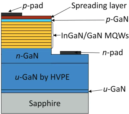
Two kinds of LED epitaxial structures were grown on c-plane sapphire substrates by combining MOCVD and HVPE growth techniques. Schematics of the fabricated LEDs are shown in figure 1. Firstly u-GaN was grown on sapphire substrates by MOCVD with nominal thickness of ∼4.5 μm, and then HVPE was employed to grow thick u-GaN. The total thickness of
the MOCVD-GaN and HVPE-GaN buffer layers is ∼12 μm and ∼30 μm, respectively, which was estimated by scanning electron microscope (SEM) images and CL mapping of the sample cross-sections. We have noticed that, in the following analysis, the GaN thicknesses in figure 3(a) are not exactly 12 μm and 30 μm, as the cross-section for CL mapping is not perfectly smooth for collecting the spectra. The LED structures of the two samples were grown simultaneously by MOCVD, and consisted of a ∼100 nm n-GaN layer, nine InGaN/GaN QWs and a 150 nm p-GaN layer. The nominal thickness of the three QWs at the bottom is 3 nm, and the nominal thickness of the latter six QWs is 4 nm. We started LED processing by depositing Ni/Au (10 nm/25 nm) on the p-GaN, after which reactive ion etching (RIE) and inductively coupled plasma (ICP) etching were used to etch the Ni/Au layers and LED epi-taxial layers down to the n-GaN, respectively. After annealing the Ni/Au in purified air to form a current spreading layer, Ti/ Au (50 nm/200 nm) layers were deposited as the p- and n-pads. The size of the fabricated LEDs is 300 μm × 270 μm.
[image:2.595.319.538.61.254.2]To evaluate the dislocation density of the GaN buffer layer, a field emission gun scanning electron microscope (FEI Sirion 200) was used to acquire room temperature CL hyperspectral images of the HVPE-GaN surface and the LED cross-section. A hyperspectral image refers to a two dimensional array of CL spectra recorded as an electron beam scans across the sample surface [14, 15]. An acceleration voltage of 5 kV, 100 nm or 150 nm scanning steps and a spot diameter of ∼2 nm were used. Each CL spectrum was then fitted by Lorentzian func-tion to get the peak energy, intensity, and width. A Renishaw inVia Raman microscope was used to measure room temper-ature photoluminescence (PL) spectra of the LED epitaxial layers using a 325 nm laser with excitation power 0.32 mW and to collect the Raman spectra of the GaN layer using a 514 nm or 633 nm laser. The laser spot size was ∼2 μm in diameter. The electroluminescence (EL) spectra were meas-ured using an Ocean Optics USB4000 spectrometer. The light output power was measured under pulsed operation with pulse duration of 100 μs and a duty cycle of 1%, to minimize the
Figure 1. Schematic structure of the LEDs grown by MOCVD and HVPE. The total thickness of u-GaN grown by MOCVD and HVPE is ∼12 μm and ∼30 μm for the two samples.
LED self-heating effect. The −3 dB modulation bandwidth was measured by driving the LED with a direct current (DC) bias and a small-signal modulation from an HP8753ES net-work analyzer. The light output power from the LED was detected by a high-speed photo detector, and the frequency response of this signal was recorded by the network analyzer.
3. Results and discussion
3.1. Characteristics of CL, PL and Raman spectra
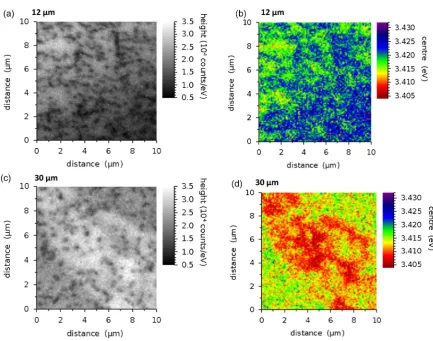
Figures 2(a)–(d) show the CL mapping results (peak intensity and peak energy) for the 12 μm and 30 μm GaN buffer sur-faces. The two samples were prepared by etching away the epi-taxial LED layers using ICP. The ICP dry etching was solely used to expose the HVPE-GaN surface in our work, although we note that dry etching may provide another approach to determining the dislocation density when followed by atomic force microscopy (AFM) [16]. The dislocations in the GaN layers play a role as nonradiative recombination centers, and relatively weak CL emission appears from these areas. By counting the dark spots in figures 2(a) and (c), the dislocation densities of the 12 μm and 30 μm GaN buffer surface are esti-mated to be ∼1.3 × 108 cm−2 and ∼1.0 × 108 cm−2, respec-tively. A previous study has used chemical etching to reveal the dislocations, followed by AFM of the surface to give the dislocation density by counting the surface pit density [17].
[image:3.595.85.519.60.401.2]In comparison, the CL mapping approach (while lacking the AFM’s resolving power for the closest-spaced disloca-tions) allows the dislocation density to be obtained without wet etching or dry etching [16, 17]; this method has previ-ously been reported by several studies [18, 19]. This shows that growing a thicker GaN buffer layer has reduced the dis-location density by ∼30%, which is expected to reduce the dislocation density of the LED epitaxial layers grown on top of the buffer layer. The dislocation density agrees with the trend for the GaN layers with different thicknesses in the literature [20]. Chen et al [17] employed growth tech-niques of patterned sapphire substrate (PSS), ex situ sputtered AlN and two-step HVPE growth to achieve interruption-free HVPE-GaN with thickness of 9.7 μm and dislocation density down to 3.45 × 108 cm−2. Although an extra step of MOCVD growth was required in our work, our method offers the potential advantages of growing high quality GaN template or inserting a special GaN layer, e.g. a heavily doped GaN layer. After removing the sapphire substrate by laser lift-off [21], the heavily-doped GaN layer can be used to form a high-quality n-type contact for vertical struc-tural LEDs. In addition, the average peak intensities of the 10 μm × 10 μm area are ∼1.6 × 10⁴ counts/eV and ∼2.4 × 10⁴ counts/eV for the 12 μm and 30 μm samples, respec-tively, which is consistent with the difference in dislocation density. In figures 2(b) and (d), the CL peak energy varies slightly across the scanned areas; however, when the buffer
P Tian et al
thickness increases from 12 μm to 30 μm, a red shift in the GaN peak energy can be observed which indicates that the compressive strain induced by the mismatch of lattice con-stants and different thermal expansion coefficients between GaN layers and sapphire substrates was relaxed [22, 23].
To further investigate the optical and stress properties of the thick buffer, CL maps of the cross-section of the thick buffer layer were obtained and figure 3(a) shows the typical linescan peak energy from the GaN/sapphire interface to the LED surface after fitting the GaN emission spectra. The peak energy shows a fast decrease until ∼5 μm and then fluctuates around 3.415 eV and 3.410 eV for the 12 μm and 30 μm sam-ples, respectively. Assuming that the compressive stress effect is the dominant influence on the energy shift in the CL spectra [22], the initial fast energy decrease suggests that the com-pressive stress has largely been relaxed by the MOCVD-GaN layer. The red shift of thicker HVPE-GaN agrees with the red shift of the surface mapping results in figure 2. The Raman spectra of the HVPE-GaN surface were obtained as shown in figure 3(b). For unstressed GaN, the E2-high mode is typically ∼568 cm−1, and the biaxial compressive stress σ (in GPa) can be calculated by the frequency shift ∆ω (in cm−1): ∆ =ω 6.2σ [24]. The E2-high modes of the 12 μm and 30 μm samples after Gaussian fitting are ∼569.2 cm−1
and ∼568.7 cm−1, respectively, indicating stress relaxation of ∼0.08 GPa with thicker buffer layer. It is expected that this relaxation of stress in the GaN buffer layer will reduce the compressive strain in the InGaN/GaN QWs.
Typical PL spectra measured from the LEDs are shown in figure 4(a). Using a Lorentz fit, the PL peak wavelengths were found to be 469 nm and 448 nm for the LEDs with 12 μm and 30 μm GaN buffers, respectively. With thicker HVPE-GaN, the surface roughness increased [17], and caused the damping of Fabry-Perot modes in the 30 μm sample. To confirm that this observed shift is due to compressive stress in the LED wafers, Raman spectra were measured from the top p-GaN layer, as shown in figure 4(b). Note that we have measured more than ten points across the LED wafers for both the PL and Raman spectra, and the results in figure 4 show typical spectra. Using a Gaussian fit, the E2-high mode was found to be ∼569.1 cm−1 and ∼568.3 cm−1 for the 12 μm and 30 μm buffer LEDs, respectively. Significant stress relaxation of ∼0.13 GPa is found for the 30 μm buffer LEDs compared with the 12 μm buffer LEDs. Compared with the stress relaxa-tion of thick buffer surface in figure 3(b), the p-GaN surface shows similar trend after growth of the LED structure. It has been reported that stress relaxation might lead to a higher indium content and a thicker QW [11, 21, 25]. However, our 520 540 560 580 600 620
0.0 0.2 0.4 0.6 0.8 1.0
Normalized Raman intensity
Wavenumber (cm-1)
12 µm 30 µm
0 5 10 15 20 25 30
3.40 3.41 3.42 3.43 3.44 3.45
CL peak energy (eV)
Distance from the GaN/sapphire interface (µm) 12 µm
[image:4.595.308.545.60.423.2]30 µm
Figure 3. (a) Typical linescan CL peak energy from the GaN/ sapphire interface to the LED surface and (b) Raman spectra of the HVPE-GaN surface of the 12 μm and 30 μm samples.
380 400 420 440 460 480 500 520 540 0.0
0.2 0.4 0.6 0.8 1.0
Nor
maliz
ed PL intensity
Wavelength (nm) 12 µm
30 µm
520 540 560 580 600 620 0.0
0.2 0.4 0.6 0.8 1.0
Nor
maliz
ed Raman intensity
Wavenumber (cm-1) 12 µm
30 µm
(a)
(b)
Figure 4. (a) Room temperature PL spectra and (b) Raman spectra of LEDs with 12 μm and 30 μm GaN buffer thickness.
[image:4.595.51.291.62.425.2]previous work showed that any variations in the QW thickness and indium content was extremely small for similar samples grown on HVPE-GaN [21], so we assume that the effects of the QW thickness and indium content are not dominant in this work. The mechanisms of the HVPE-GaN stress effect on the LED growth will be further investigated in our future work. Thus, we conclude that the large blue shift (21 nm) observed in the PL peak is mainly caused by the QCSE effect and that the related compressive stress in the QWs was reduced after increasing the GaN buffer thickness.
[image:5.595.304.551.53.226.2] [image:5.595.51.301.64.422.2] [image:5.595.319.539.270.429.2]3.2. Characteristics under electrical injection
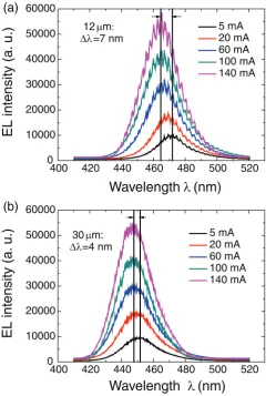
Figure 5 shows the EL spectra of these LEDs at currents from 5 mA to 140 mA, where 140 mA corresponds to a current den-sity of ∼173 A cm−2. The effect of increasing the buffer thick-ness is to cause a large blue shift in the EL peak wavelength from ∼470 nm to ∼450 nm, in agreement with the PL results in demonstrating stress relaxation of the InGaN MQWs. An additional blue shift in the EL is seen with increasing current; this is caused by carrier screening and band filling effects, while a smaller blue shift with current increase, from 7 nm to 4 nm with increasing buffer thickness, indicates a relatively weaker piezoelectric field inside the MQWs. This smaller blue shift for the LED with the 30 μm GaN buffer further
confirms that the compressive strain relaxation has been greatly reduced.
The light output powers were then measured and the corre-sponding EQEs were calculated as shown in figure 6. With buffer thickness increase, the EQE improves significantly by 50% at 20 mA and 16% at 140 mA. Here we assume the light extraction efficiency is similar for the two samples and the difference of EQE is mainly caused by the internal quantum efficiency (IQE). On the one hand, the dislocation density reduction in the LED with a thicker buffer layer may lead to a decrease in the defect-related Shockley–Read–Hall (SRH) recombination rate, most significantly affecting the EQE at low currents (approximately those below the EQE peak, e.g. 20 mA) [8–10]. On the other hand, stress relaxation causes a large efficiency increase of the LED with a thicker buffer layer. At a high current, e.g. 140 mA, the SRH recombination is no longer dominant due to the increased effects of radia-tive recombination, Auger recombination, electron leakage and other effects [8–10], and thus the strain relaxation plays a more important role than the defect effect. However, due to the carrier screening and band filling effects, the piezo-electric field caused by the QCSE was weaker at a higher current, which explains the smaller efficiency improvement at high current densities. In addition, the 30 μm LED may 400 420 440 460 480 500 520
0 10000 20000 30000 40000 50000 60000
EL intensity (a.
u.)
Wavelength
λ
(nm)
5 mA 20 mA 60 mA 100 mA 140 mA 12 µm:∆λ=7 nm
400 420 440 460 480 500 520 0 10000 20000 30000 40000 50000 60000
30 µm:
∆λ=4 nm
EL intensity (a.
u.)
Wavelength
λ
(nm)
5 mA 20 mA 60 mA 100 mA 140 mA(a)
(b)
Figure 5. EL spectra of LEDs from 5 mA to 140 mA with (a) 12 μm and (b) 30 μm GaN buffer thickness.
0 20 40 60 80 100 120 140 160
0 10 20 30 40 50 60 70
12 µm
16% 30 µm
Current (mA)
Light output po
wer (a. u.) 50% 0.4 0.5 0.6 0.7 0.8 0.9 1.0 Nor maliz ed EQE
Figure 6. Light output power and EQE versus current for LEDs with (a) 12 μm and (b) 30 μm GaN buffer thicknesses.
0 20 40 60 80 100 20 40 60 80 100 120 Bandwidth (MHz) Current (mA) 12 µm
30 µm
P Tian et al
have slightly thicker QWs and higher indium content [21]. A thicker QW could reduce the rate of Auger recombination and increase the LED efficiency at a high current density [26]. A higher indium content may cause a larger QCSE and In phase separation, leading to efficiency reduction [27]. However, as discussed above, the QCSE effect is likely to dominate over the effects of MQW thickness and the InN content. We thus conclude that using a thicker buffer layer will be an effective approach to improving the efficiency for the SLL.
3.3. Characteristics of modulation bandwidth
The electrical-to-optical −3 dB modulation bandwidth versus current characteristics of the LEDs are shown in figure 7. With the buffer thickness increase, it is found that the bandwidth decreased by ∼40% at low current (e.g. 5 mA) and by ∼10% at high current (e.g. 100 mA). The modulation bandwidth f3 dB
can be expressed by f3 dB = 3 2/ πτ, where τ represents the differential lifetime and is related to the carrier concentration
n by the equation [8, 28],
A Bn Cn
1 2 3 2
τ = + +
(1)
where A, B and C represent the coefficients of defect-related SRH recombination, radiative recombination, and high-order non-radiative recombination, respectively. The total current I
can be expressed as
I=qVactive(An+Bn2+Cn3),
(2) where the q represents the electron charge and Vactive the effec-tive volume of QWs in the aceffec-tive region. At low currents (e.g. we choose currents less than 5 mA in this study), the defect recombination (linear term) and radiative recombination (qua-dratic term) dominate, and then we can derive
A B
qV I
1 4 .
2 2
active
τ = +
(3)
Through fitting 1/τ2 versus I from 1 mA to 5 mA, the A coef-ficients were obtained to be ∼8.5 × 10⁷ s−1 and ∼4.4 × 10⁷ s−1 for LEDs with 12 μm and 30 μm GaN buffers, respectively, which supports the conclusion of increased defect-related SRH recombination for the thicker buffer LED in figure 6. The higher SRH recombination in the QWs can lead to a higher modulation bandwidth which provides a possible approach to designing high-speed LEDs for VLC, but causes lower light output power and EQE. The competition between these two effects needs to be considered in practical applications in SSL and VLC.
4. Conclusion
We have fabricated and characterized GaN-based LEDs with different GaN buffer thicknesses of 12 μm and 30 μm grown by combining HVPE and MOCVD techniques. With increasing the buffer layer thickness, the dislocation density in the buffer layer decreases from ∼1.3 × 108 cm−2 to ∼1.0 × 108 cm−2, confirmed by CL hyperspectral imaging. A compressive stress
relaxation is confirmed by Raman spectroscopy and leads to a large blue shift in peak emission wavelength of the PL and EL. The effects of reduced dislocation density and stress relax-ation produce an improved efficiency for the LED with 30 μm buffer thickness. A rate equation analysis shows the defect-related nonradiative recombination can help increase the mod-ulation bandwidth of the LED with 12 μm buffer thickness at low current, suggesting an approach for increasing the modu-lation bandwidth for VLC.
Acknowledgments
This work was supported by a UK Engineering and Physical Sciences Research Council grant EP/K00042X/1, Start-up Research Funding JJH1232106 from Fudan University, and State Key Laboratory of Luminescence and Applications funding SKLA201619. The data presented in this paper is available at
https://doi.org/10.15129/68e2f7a9-36ea-4598-a163-b8b440b593db. We acknowledge Dr Ian M Watson
for the fruitful discussions on determining the dislocation density.
References
[1] Pimputkar S, Speck J S, DenBaars S P and Nakamura S 2009
Nat. Photon.3 180
[2] Rajbhandari S et al 2015 IEEE J. Sel. Areas Commun.33 1750
[3] Jeong J W et al 2015 Cell162 662
[4] Tian P et al 2014 J. Appl. Phys.115 033112
[5] Kim T et al 2012 Small8 1643
[6] Li K H, Cheung Y F, Cheung W S and Choi H W 2015 Appl.
Phys. Lett.107 171103
[7] Trindade A J et al 2015 Opt. Express23 9329
[8] Verzellesi G, Saguatti D, Meneghini M, Bertazzi F, Goano M, Meneghesso G and Zanoni E 2013 J. Appl. Phys.
114 071101
[9] Cho J, Schubert E F and Kim J K 2013 Laser Photonics Rev. 7 408
[10] Schubert M F, Chhajed S, Kim J K, Schubert E F, Koleske D D, Crawford M H, Lee S R, Fischer A J, Thaler G and Banas M A 2007 Appl. Phys. Lett.91 231114
[11] Johnson M C, Bourret-Courchesne E D, Wu J, Liliental-Weber Z, Zakharov D N, Jorgenson R J, Ng T B, McCready D E and Williams J R 2004 J. Appl. Phys. 96 1381
[12] Sochacki T et al 2014 J. Cryst. Growth394 55
[13] Schubert E F 2006 Light Emitting Diodes 2nd edn (Cambridge: Cambridge University Press) p 396 [14] Edwards P R and Martin R W 2011 Semicond. Sci. Technol.
26 064005
[15] Edwards P R, Jagadamma L K, Bruckbauer J, Liu C, Shields P, Allsopp D, Wang T and Martin R W 2012
Microsc. Microanal.18 1212
[16] Choi H W, Liu C, Cheong M G, Zhang J and Chua S J 2005
Appl. Phys. A 80 405
[17] Chen Y A, Kuo C H, Wu J P and Chang C W 2015 J. Cryst.
Growth426 180
[18] Naresh-Kumar G et al 2014 Microsc. Microanal.20 55
[19] Meissner E, Schweigard S, Friedrich J, Paskova T, Udwary K, Leibiger G and Habel F 2012 J. Cryst. Growth340 78
[20] Bennett S E 2010 Mater. Sci. Technol.26 1017
[21] Li J Z, Tao Y B, Chen Z Z, Jiang X Z, Fu X X, Jiang S, Jiao Q Q, Yu T J and Zhang G Y 2013 Chin. Phys. B 23 016101
[22] Siegle H, Hoffmann A, Eckey L, Thomsen C, Christen J, Bertram F, Schmidt D, Rudloff D and Hiramatsu K 1997
Appl. Phys. Lett.71 2490
[23] Lethy K J, Edwards P R, Liu C, Wang W N and Martin R W 2012 J. Appl. Phys.112 023507
[24] Kozawa T, Kachi T, Kano H, Nagase H, Koide N and Manabe K 1995 J. Appl. Phys.77 4389
[25] Pereira S, Correia M R, Pereira E, O’donnell K P,
Trager-Cowan C, Sweeney F and Alves E 2001 Phys. Rev. B 64 205311
[26] Gardner N F, Müller G O, Shen Y C, Chen G, Watanabe S, Götz W and Krames M R 2007 Appl. Phys. Lett.91 243506
[27] Shin D S, Han D P, Oh J Y and Shim J I 2012 Appl. Phys. Lett. 100 153506
[28] Olshansky R, Su C B, Manning J and Powazinik W 1984