Rochester Institute of Technology
RIT Scholar Works
Theses Thesis/Dissertation Collections
8-2-2017
The Influence of Alternative Electrode
Configurations and Process Integration Schemes
on IGZO TFT Operation
Eli P. Powell
Follow this and additional works at:http://scholarworks.rit.edu/theses
This Thesis is brought to you for free and open access by the Thesis/Dissertation Collections at RIT Scholar Works. It has been accepted for inclusion in Theses by an authorized administrator of RIT Scholar Works. For more information, please [email protected].
Recommended Citation
on IGZO TFT Operation
The Influence of Alternative Electrode
Configurations and Process Integration Schemes
on IGZO TFT Operation
Eli P. Powell
August 2, 2017
A Thesis Submitted in Partial Fulfillment
of the Requirements for the Degree of Master of Science
in
Microelectronic Engineering
on IGZO TFT Operation
Eli P. Powell
Committee Approval:
Dr. Karl HirschmanAdvisor Date
Professor
Dr. James Moon Date
Professor
Dr. Ivan Puchades Date
Assistant Professor
Dr. Robert Pearson Date
Acknowledgments
I would like to acknowledge and thank everyone whose guidance and support made
this project possible. Firstly, my advisor Dr. Karl Hirschman, for his support and
guidance throughout my time at RIT and throughout this project. My committee
members, Dr. James Moon and Dr. Ivan Puchades, for the guidance that they
like-wise provided. I would also like to thank the members of the Team Eagle research
group for their support and assistance in processing and data collection: Tarun
Mud-gal, Prashant Ganesh, Julia Okvath, Patricia Meller, and the rest of Team Eagle. I
would also like to thank the SMFL staff: Sean OBrien, John Nash, Rich Battaglia,
Bruce Tollesen, Peter Morici, Scott Blondell and Tom Grimsley, for without their
hearts and minds of all those that he touched. Thank you for everything you’ve done
for me and know that I will always appreciate and love you. May you rest in peace
Abstract
Amorphous oxide semiconductors (AOS) have been extensively studied for their
appli-cation in thin-film electronics; an area which is currently dominated by hydrogenated
amorphous silicon (a Si:H) technology. Indium-gallium-zinc oxide (IGZO) has
gar-nered most of the AOS materials focus due to its high carrier mobility and process
simplicity. When modifying an existing process flow for fabrication of TFTs, the
effect of each modification on the electrical characteristics must be determined. The
compatibility of the process with the constraints of a glass substrate must also be
considered. A new test chip layout was created that enables the fabrication of TFTs
with a variety of electrode configurations including top-gate, bottom-gate,
double-gate, and either staggered or co-planar source/drain regions. TFTs were fabricated
on glass and oxidized silicon substrates, consisting of sputter-deposited IGZO
sur-rounded by SiO2 dielectric layers, an oxidizing ambient anneal treatment, and a
capping layer deposited by atomic layer deposition (ALD). Electrical characteristics
from each process treatment and gate configuration were compared, with some noted
differences in device operation related to process integration. A SPICE level 2
com-patible IGZO TFT model was developed, with extracted parameter values providing
Signature Sheet i
Acknowledgments ii
Dedication iii
Abstract iv
Table of Contents v
List of Figures viii
List of Tables xi
List of Symbols xii
1 Literature Review 1
1.1 Background . . . 1
1.2 Current Technology and Limitations . . . 2
1.3 Candidates to Replace hydrogenated amorphous silicon (a-SI:H) . . . 4
1.4 Brief History of Oxide-Semiconductors . . . 5
1.5 Motivation For The Development of Indium Gallium Zinc Oxide (IGZO) Thin-Film Transistors (TFTs) . . . 6
2 Preliminary Research 8 2.1 Device Fabrication . . . 8
2.2 Device Performance . . . 9
2.2.1 Long-Channel Behavior . . . 9
2.2.2 Bias Stress Response . . . 10
2.3 1-D Device Model . . . 12
2.3.1 Initial Model . . . 12
2.3.2 Model Refinement . . . 14
2.4 Terada-Muta Analysis of IGZO TFTs . . . 15
CONTENTS
3 Single and Double Gate TFTs 17
3.1 New Mask Design . . . 17
3.2 Device Fabrication . . . 19
3.3 Bottom Gate TFTs . . . 22
3.4 Double Gate with Staggered Bottom Gate (DGBS) TFTs . . . 24
3.4.1 Electrical Characteristics . . . 24
3.4.2 Summary of Results DGBS . . . 26
3.5 Double Gate with Staggered Top Gate (DGTS) TFTs . . . 27
3.5.1 Electrical Characteristics . . . 27
3.5.2 Summary of Results DGTS . . . 29
3.6 Staggered Top Gate (TGS) TFTs . . . 30
3.6.1 Electrical Characteristics . . . 30
3.6.2 Summary of ResultsT GS . . . 32
3.7 Coplanar Top Gate (TGC) TFTs . . . 33
3.7.1 Electrical Characteristics . . . 33
3.7.2 Summary of ResultsT GC . . . 35
3.8 Evaluation of Electrode Configurations . . . 36
3.8.1 Bias Stress Stability . . . 37
3.9 Summary of Single and Double Gate TFTs . . . 42
4 Comprehensive Device Model 44 4.1 Motivation . . . 44
4.2 Refinement of Spice Level 2 Model . . . 45
4.2.1 Initial Model Shortcoming . . . 45
4.2.2 Two Dimensional Charge Model . . . 46
4.2.3 Short Channel Refinement . . . 47
4.3 Methodology . . . 48
4.4 Analysis of Fabricated Devices . . . 52
4.4.1 Double Gate with Staggered Bottom Gate . . . 52
4.4.2 Double Gate with Staggered Top Gate . . . 53
4.4.3 Staggered Top Gate . . . 54
4.4.4 Coplanar Top Gate . . . 55
4.5 Summary . . . 57
5 Conclusions 58 5.1 Summary of Work . . . 58
Bibliography 61
Acronyms 63
A Parameter Extraction Matlab Code 64
B Process Recipies 70
List of Figures
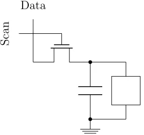
1.1 Equivalent circuit of active matrix display. A liquid crystal and
stor-age capacitor are connected in parallel being driven by a TFT that is
connected to the scan and data circuits. . . 2
1.2 Mobility requirements for current and future displays . . . 3
1.3 Active matrixVT compensation circuit utilizing 4 TFTs and 2 storage
capacitors [5]. . . 4 1.4 Comparison of a-Si:H and un-passivated IGZO TFT ID-VGS transfer
characteristics with dimensions ofW/L= 30/5 µm andW/L= 100/48
µm, respectively. [10, 11]. . . 7
2.1 Cross-section schematics of bottom and double-gate TFTs. The
bot-tom gate device has staggered gate-source/drain electrodes. The
double-gate device has the staggered electrode configuration of the bottom
gate device, with the addition of a co-planar top gate. . . 9
2.2 Transfer characteristics of long-channel (L= 24 µm) devices with
bot-tom (left) and double (right) gate electrode configurations. . . 10 2.3 Response of bottom gate devices to a) positive bias stress and b)
neg-ative bias stress . . . 11
2.4 Response of double-gate devices to a) positive bias stress and b)
nega-tive bias stress. (c) Double gate device transfer characteristic voltage
shift over time under negative and positive bias stress. . . 12
2.5 Measured and modeled linear ID-VGS transfer characteristics. . . 13
2.6 Measured and modeled linear and saturation ID-VGS transfer
charac-teristics. The measured data and model are represented by circles and
a solid line, respectively. . . 14 2.7 Terada-Muta analysis of IGZO TFTs. . . 15
2.8 S/D lift-off lithography bias with a mask defined channel length of 6µm. 15
3.1 An image of the new reticle design for IGZO TFTs. This reticle enables
all electrode configurations to be present on one wafer. . . 18
3.3 A step by step illustration of device fabrication. Process flow is as
follows: a) Barrier oxide growth, b) Bottom gate deposition and
pat-terning, c) Bottom gate dielectric deposition, d) DGTS S/D deposition
and patterning, e) IGZO deposition and patterning, f) DGBS S/D de-position and patterning, g) Top gate dielectric dede-position, and h) Top
gate deposition and patterning. An ALD capping layer can be
de-posited on top of either or both gate dielectric. . . 20
3.4 Fabrication results in a) double-gate from top gate on the left hand
half and b) double-gate from bottom gate on the right hand half of
the wafer. c) An optical microscope image of a double-gate with a
staggered bottom gate IGZO TFT. . . 21
3.5 ID-VGS transfer characteristics of staggered bottom gate devices, with
different rest times. . . 22
3.6 ID-VGS transfer characteristics of W/L = 24/24µm double-gate from
bottom gate TFTs. . . 24
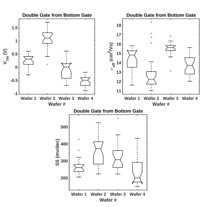
3.7 Box plots of extracted parameters for DGBS on wafers 1−4. . . 25
3.8 ID-VGS transfer characteristics of W/L = 24/24µm double-gate from
top gate TFTs. . . 27
3.9 Box plots of extracted parameters for DGTS on wafers 3−4. . . 28
3.10 ID-VGS transfer characteristics ofW/L= 24/24µm staggered top gate
TFTs. . . 30
3.11 Box plots of extracted parameters for T Gstg on wafers 3−4. . . 31
3.12 ID-VGS transfer characteristics of W/L = 24/24µm coplanar top gate
TFTs. . . 33
3.13 Box plots of extracted parameters for T Gcop on wafers 1−4. . . 34
3.14 ID-VGStransfer characteristics ofW/L= 24/24µm devices with a glass
substrate and ALD capping layer. . . 36
3.15 Extracted parameters from W/L=24/24µm devices with a glass
sub-strate and ALD capping layer. . . 37
3.16 Negative (right) and positive (left) bias stress response for devices of
W/L= 24/24µm for DGBS configuration of wafer three and four. . 38
3.17 Negative (right) and positive (left) bias stress response for devices of W/L= 24/24µm for DGTS configuration of wafer three and four. . . 39
3.18 Negative (right) and positive (left) bias stress response for devices of
LIST OF FIGURES
3.19 Negative (right) and positive (left) bias stress response for devices of
W/L= 24/24µm for TGC configuration of wafer three and four. . . . 41
4.1 Linear ID-VGS measurements of a-SI:H (left) and IGZO (right) TFTs. 45
4.2 Representative issue with initial device model. Even though a good transfer match is observed a match with the family is not guaranteed. 46
4.3 Device models for a 6µm BGS TFT with (right) and without (left)
consideration towards channel-length modulation. The model fit is
represented by a dashed line and the data is represented by a solid line. 48
4.4 Detailed Flowchart of Parameter Extraction Method . . . 50
4.5 Overlay of transfer and output characteristics of measured data and the
presented model. Transfer characteristics are shown in linear mode (a)
with VDS = 0.1 V, and saturation mode (b) with VDS = 10 V. (c)
Output characteristics withVGS = 2-10 V in steps of 2 V. In all plots
data is represented by points and the fit is a solid line. . . 51
4.6 Family of curves for double-gate with staggered bottom gate with
W/L=24/6 for each treatment. . . 53
4.7 Family of curves for double-gate with staggered top gate withW/L=24/6
for each treatment. . . 54
4.8 Family of curves for staggered bottom gate with W/L=24/6 for each
treatment. . . 55
4.9 Family of curves for coplanar bottom gate with W/L=24/6 for each
1.1 Comparison of a-SI:H, Poly-Si, and a-IGZO as TFT channel materials
[2, 4]. . . 5
3.1 Summary table of fabrication differences between each wafer. All
wafers contain all possible device configurations. . . 21
3.2 Extracted electrical characteristics of W/L = 24/24µm double-gate from bottom gate TFTs. . . 25
3.3 Extracted electrical characteristics of W/L = 24/24µm double-gate
from top gate TFTs. . . 28
3.4 Extracted electrical characteristics ofW/L = 24/24µm staggered top
gate TFTs. . . 31
3.5 Extracted electrical characteristics of W/L = 24/24µm coplanar top
gate TFTs. . . 34
3.6 Bias stress conditions. . . 38
3.7 A qualitative summary of all electrical tests carried out on all electrode
configurations. . . 43
4.1 Parameters extracted from a staggered bottom gate device withW/L=100/12µm 51
4.2 Parameters extracted from double-gate with staggered bottom gate
of each treatment with length of 6 microns and width of 24 microns.
Parameters were extracted using the method described in Sec. 4.3. . . 52
4.3 Parameters extracted from double-gate with staggered top gate of each
treatment with length of 6 microns and width of 24 microns.
Parame-ters were extracted using the method described in Sec. 4.3. . . 54
4.4 Parameters extracted from staggered top gate of each treatment with length of 6 microns and width of 24 microns. Parameters were
ex-tracted using the method described in Sec. 4.3. . . 55
4.5 Parameters extracted from coplanar top gate of each treatment with
length of 6 microns and width of 24 microns. Parameters were
ex-tracted using the method described in Sec. 4.3. . . 56
List of Symbols
Term Description Units/Value
Cox0 Oxide capacitance per unit area F/cm2
Eg Band gap energy eV
EOV Energy of oxygen vacancies eV
gm Transconductance S
ID Drain current A
L Channel length µm
NOV Energy density of oxygen vacancies cm−3eV−1
NT A Energy density of acceptor-like tail-states cm−3eV−1
NT D Energy density of donor-like tail-states cm−3eV−1
RSD Source/Drain series resistance Ω
SS Subthreshold swing V/dec
VDS Drain–Source voltage V
VGS Gate-Source Voltage V
VR Series resistance voltage drop V
VT Threshold voltage V
W Channel width µm
WOV Width of oxygen vacancies (gaussian distribution) eV
WT A Width of acceptor-like tail-states (gaussian
distri-bution)
eV
WT D Width of donor-like tail-states (gaussian
distribu-tion)
eV
χ Electron affinity eV
IGZO Relative permittivity of IGZO
∆VG Sub-threshold separation V
µ0 Intrinsic electron mobility cm2/Vs
µ0 Effective electron mobility cm2/Vs
µT H Threshold mobility cm2/Vs
Literature Review
1.1
Background
Prior to the development of active-matrix LCDs (AM-LCDs) the passive-matrix was
the standard for LCDs. In a passive matrix LCD, a grid is created by using one glass
substrate to address the rows and the other substrate to address the columns. In
order to turn on a pixel, a voltage signal is sent to the corresponding column and
the respective row is grounded to complete the circuit. However, direct addressing
of the pixel has two major drawbacks; slow response time and poor voltage control.
Also, when directly addressing a pixel a leakage path is present that allows adjacent
pixels to be turned on. On the other hand, an active matrix LCD addresses the pixel
through a transistor which eliminates the leakage paths. As such, AM-LCDs have
dominated the display industry. An example of a simple active-matrix circuit can be
seen in Fig. 1.1 which consists of a switching Thin-Film Transistor (TFT), storage
capacitor, and liquid crystal.
In order for a pixel to be turned on in an AM-LCD there must be an appropriate
voltage applied to the data line and the pixel must be addressed through the scan
line. Once the storage capacitor has fully charged the scan line is disconnected, thus
the pixel is no longer addressed, and the TFT is turned off. Voltage is maintained
across the liquid-crystal by the storage capacitor until the pixel is addressed again.
CHAPTER 1. LITERATURE REVIEW
Data
[image:17.612.256.399.86.220.2]Scan
Figure 1.1: Equivalent circuit of active matrix display. A liquid crystal and storage capacitor are connected in parallel being driven by a TFT that is connected to the scan and data circuits.
the liquid crystal, thus allowing a precise amount of light through the display. For
organic light-emitting diode (OLED) displays precise control of pixel illumination can
be achieved by controlling current injected into the OLED.
With advances in display technology, more stringent manufacturing and
perfor-mance requirements are necessary. As display technology progresses to generation 10,
which uses a substrate that is roughly 3 m×3 m, large area uniformity becomes a major
concern. Electrical uniformity requirements are more demanding for OLED displays
due to the high sensitivity of brightness on the drain current of the driving TFT.
Another requirement is that the semiconductor material must be low-temperature
compatible, as they are typically fabricated on glass substrates with a thermal
tol-erance around 600◦C. Finally, with decreasing aspect ratios in high pixel density
displays it is advantageous for TFTs to be transparent to visible light.
1.2
Current Technology and Limitations
In the semiconductor industry, crystalline silicon is the undisputed leading technology
platform. As a result silicon has been extensively studied over the past 60 years
making it the most understood semiconducting material. Not surprisingly silicon
silicon, thin-film hydrogenated amorphous silicon (a-SI:H) is the channel material for
TFTs.
The use of a-SI:H is attractive as it is low-temperature compatible and can be
deposited with plasma-enhanced chemical-vapor deposition (PECVD) below 350◦C.
It has good large area uniformity due to its amorphous structure and it is a well
[image:18.612.174.476.233.466.2]understood, low-cost material.
Figure 1.2: Mobility requirements for current and future displays [1].
Several challenges emerge with the demanding requirements of next generation
displays. High pixel density displays and fast switching speed applications require
a high-mobility semiconductor for improved current drive to minimize delay times
[2, 3]. A 50-inch AM-LCD with copper bus lines was used to determine the estimated
mobility requirements shown in Fig. 1.2. These values roughly double when
consider-ing a 70-inch AM-LCD due to increased delay times [1]. This is a major drawback for
a-SI:H whose mobility is around 1 cm2/V s. Another disadvantage with a-SI:H is its bias stress instability. A 20 % change in brightness can occur if the driving TFTs VT
CHAPTER 1. LITERATURE REVIEW
light emitting diodes (OLEDs). While compensation circuits exist which cancel out
VT errors exist and make it possible to use a-SI:H as an OLED driver, the added
complexity reduces yield, driving costs up. One example of such a circuit can be seen
[image:19.612.219.432.183.398.2]in Fig. 1.3.
Figure 1.3: Active matrixVT compensation circuit utilizing 4 TFTs and 2 storage
capac-itors [5].
1.3
Candidates to Replace a-SI:H
In order to meet the driving demand of the display industry, several candidates to
replace a-SI:H are being investigated; some can be seen in Table 1.1. Low-temperature
polycrystalline silicon (LTPS) fulfills the mobility requirements and is at least an order
of magnitude greater than its amorphous counterpart. It is also stable enough under
bias stress that it can be used to drive OLEDs without a compensation circuit. Also,
as a result of the fabrication process CMOS transistors are able to be realized and as
such their benefits may be utilized. LTPS is formed by depositing a-SI:H and then
crystallized by excimer laser annealing (ELA). This technique is appealing because of
with this process are the high cost and large-scale electrical uniformity issues. As such,
it is a suitable candidate for small form displays like cellphones and tablets rather
than larger substrates, like Gen 10 displays. Amorphous-oxide semiconductors, such
as IGZO, are another contender to replace a-SI:H. This is due to their high electron
mobility compared to a-SI:H. These materials can have a lower density of tail-states
associated with the conduction band making them less sensitive to bias stress than
a-SI:H [2, 4]. They also don’t suffer from electrical non-uniformities like LTPS due
to their amorphous structure and are low-temperature compatible. As such, unlike
LTPS, they are suitable candidates for large form displays.
Table 1.1: Comparison of a-SI:H, Poly-Si, and a-IGZO as TFT channel materials [2, 4].
Channel Material TFT Type Channel Mobility
(cm2/V s) Leakage Current TFT Uniformity
a-Si:H NMOS <1 Good Good
LTPS CMOS >100 Fair Fair
IGZO NMOS ≈10 Excellent Good
1.4
Brief History of Oxide-Semiconductors
The first oxide-semiconductors came into use after the publication of a CdS TFT
in 1962 [6]. Following this, several binary TFTs were demonstrated including In2O3
in 1964, ZnO in 1968 and SnO2 in 1970. The first AM-LCD was demonstrated in
1973 using CdSe TFTs and following this a-SI:H took over the market. ZnO saw
revitalized interest in 2003 when shortcomings of a-SI:H TFTs were first becoming
apparent. Since then several new ternary and quaternary AOS have been developed
to address electrical performance and stability challenges present in binary
CHAPTER 1. LITERATURE REVIEW
1.5
Motivation For The Development of IGZO TFTs
Amorphous indium-gallium-zinc-oxide (a-IGZO) is a promising material that has
gained interest in the flat panel display (FPD) industry due to its high electron
mobility, which is about an order of magnitude larger than a-SI:H and similar to
that of ZnO. The 4 atom composition frustrates crystallization even under higher
temperature annealing (≥400◦C). This is in contrast to ZnO and as a result the
film can achieve better large area uniformity while being deposited by sputtering.
The threshold voltage of IGZO is also much lower than ZnO. It is hypothesized that
this is due to gallium suppression of the free electrons [7]. IGZO is low-temperature
deposition compatible and exhibits high ON/OFF current ratios [2, 4]. IGZO is also
less sensitive to illumination induced instability than a-SI:H, resulting in improved
device reliability. Additionally it is compatible with processing techniques currently
used with a-SI:H ensuring a quick transition when integrating with high-volume
man-ufacturing at a low cost [2, 3, 8]. AOS are typically more stable than a-SI:H with
regard to temperature bias stress, and illumination bias stress testing. This is the
result of a lower number of tail states near the conduction band [9]. The
perfor-mance improvement of IGZO over a-Si:H is especially evident in Fig. 1.4 where, when
normalized by device width the IGZO TFT current drive is approximately 1.5 times
larger than the a-Si:H TFT despite being roughly 10 times longer in channel length.
This allows IGZO devices to operate at lower voltages and can result in reduced power
Figure 1.4: Comparison of a-Si:H and un-passivated IGZO TFT ID-VGS transfer
charac-teristics with dimensions ofW/L= 30/5 µm andW/L= 100/48µm, respectively. [10, 11].
Several challenges with a-IGZO must be overcome before it is widely adopted in
the flat panel display industry. Storage ambient could cause the electrical properties
of the film to change, necessitating a passivation material being deposited on the
back-channel of a bottom-gate TFT to ensure device stability. IGZO is not a
chem-ically robust material, necessitating lift-off processing following the active area etch.
Process-induced damage is also a concern whenever plasma processes are considered
Chapter 2
Preliminary Research
This chapter will provide an overview of the preliminary research that was performed.
This consists of a discussion of bottom- and double-gate device fabrication and their
respective electrical characteristics. The bottom gate device was staggered with a
TEOS passivation layer and the double gate device was a staggered passivated bottom
gate with the addition of a coplanar top gate. The response of these devices to bias
stress will be discussed. Finally, proposed mechanisms for voltage shifts due to bias
stress will be explored.
2.1
Device Fabrication
In order to simulate a glass substrate a 6-inch Si wafer is oxidized. A 50 nm Mo gate
is sputter deposited and then patterned by subtractive wet etch. A 100 nm SiO2 gate
dielectric is deposited by plasma-enhanced chemical-vapor deposition (PECVD), with
TEOS as the precursor. The dielectric is then densified in a nitrogen ambient for 2
hours at 600◦C. A 50 nm IGZO film is deposited by RF sputter from a target with
an In:Ga:Zn:O atomic ratio of 1:1:1:4, and then patterned by subtractive etching in
a dilute HCl mixture. Gate contacts are patterned and etched in 10:1 buffered HF.
A 300 nm Mo/Al bilayer is deposited by DC sputter for a source and drain region
having been previously defined by lift-off processing. A 100 nm SiO2 passivation layer
is then deposited by PECVD, with TEOS as the precursor. A 4-hour anneal in an
contact regions were opened, and top-gate electrodes were then defined for double
gate devices using evaporated aluminum with a lift-off resist process. Source/drain
contacts were then opened for electrical probing. A top-down micrograph and
cross-sectional illustration of the resulting structure may be seen in Fig. 2.1.
Figure 2.1: Cross-section schematics of bottom and double-gate TFTs. The bottom gate device has staggered gate-source/drain electrodes. The double-gate device has the staggered electrode configuration of the bottom gate device, with the addition of a co-planar top gate.
2.2
Device Performance
Electrical testing was done on TFT structures using an HP-4156 parameter analyzer.
TFT channel dimensions were width of 100 µm and length as indicated. All ID
-VGS transfer characteristics presented were taken with a gate voltage up-sweep unless
otherwise noted, with low-drain and high-drain bias conditions at 0.1 V and 10 V,
respectively.
2.2.1 Long-Channel Behavior
The transfer characteristics of long-channel (L = 24 µm) bottom and double-gate
TFTs fabricated using the process flow described in 2.1 are shown in Fig. 2.2. The
bottom gate device demonstrated weak control over back-channel interface traps, with
a relatively shallow sub-threshold and DIBL-like separation between low-drain and
high-drain characteristics. The double-gate device demonstrated steep sub-threshold,
a threshold voltage that is right shifted from the BG device, as expected, and added
CHAPTER 2. PRELIMINARY RESEARCH
Figure 2.2: Transfer characteristics of long-channel (L = 24 µm) devices with bottom (left) and double (right) gate electrode configurations.
2.2.2 Bias Stress Response
After initial transfer characteristics were collected the response of 24 µm devices to
negative (NBS) and positive (PBS) bias stress was observed. The gate was held at
-10 V and 10 V with all other terminals at 0 V for negative and positive bias stress,
respectively. Measurements were taken at various intervals over an accumulated time
of 10,000 seconds under bias-stress. Under positive bias stress the bottom gate device
showed a negligible shift; however, negative bias stress resulted in a pronounced left
shift, approximately 1.5 V, as shown in Fig. 2.3. The pre-stress characteristic indicates
poor control over interface traps as shown by a shallow sub-threshold slope. Time
under negative bias stress appears to ionize oxygen vacancies which manifests as fixed
positive charge. As such, a lower gate voltage for electron channel charge results in a
left shift in threshold voltage[12]. Sub-threshold slope steepening was also observed
and is attributed to fixed charge behavior; fewer interface traps filling and emptying,
Figure 2.3: Response of bottom gate devices to a) positive bias stress and b) negative bias stress
Double-gate devices, on the other hand, exhibited a significant parallel right shift
in transfer characteristics under both negative and positive bias stress, as shown in
Fig. 2.4. Due to the overlapped co-planar top-gate and source/drain electrodes the
double-gate devices experience electron injection and trapping in the oxide regions
between those overlapped terminals. This effect is hypothesized to be responsible
for the parallel right shift observed under positive bias stress. Similar to positive
bias stress, the double-gate device also experiences charge injection and trapping in
the oxide regions under negative bias stress, which supports a right-shift; however
the magnitude of the observed shift is less than that under positive bias stress. It is
hypothesized that the negative bias stress left shift response of the bottom gate device
is simultaneously operative on the double-gate device. The resulting stress response
CHAPTER 2. PRELIMINARY RESEARCH
Figure 2.4: Response of double-gate devices to a) positive bias stress and b) negative bias stress. (c) Double gate device transfer characteristic voltage shift over time under negative and positive bias stress.
2.3
1-D Device Model
2.3.1 Initial Model
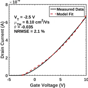
A SPICE level-2 model which uses an effective mobility model to account for mobility
enhancement, was derived. This model was developed starting with (2.1).
IDlin = W
LµCox
0
(VGS−VT)VDS (2.1a)
IDsat = W
LµCox
0(VGS−VT)
2
2 (2.1b)
where an effective mobility model, shown in (2.2), is used to account for the normal
field mobility enhancement seen in a-IGZO by allowing the fitting parameter,θ to be
negative.
µ= µT H
1 + (VGS−VT)θ
This substitution for mobility results in (2.3).
IDlin = W L−∆L
µT H
1 + (VGS−VT)θ
Cox0(VGS−VT)VDS (2.3a)
IDsat = W L−∆L
µT H
1 + (VGS−VT)θ
Cox0
(VGS−VT)2
2 (2.3b)
Using a least mean squares method the threshold voltage, field-dependent mobility,
and theta term were extracted. An example fit for the linear mode of operation can
be seen in Fig. 2.5.
-5
0
5
10
Gate Voltage (V)
0
2
4
6
8
Drain Current (A)
×
10
-6V
T
= -2.5 V
µ
TH
= 8.10 cm
2
/Vs
θ
= -0.035
NRMSE = 2.1 %
[image:28.612.165.470.289.594.2]Measured Data
Model Fit
CHAPTER 2. PRELIMINARY RESEARCH
2.3.2 Model Refinement
Even though the initial model was able to describe on-state behavior it had one major
flaw. Linear and saturation were coupled together with a common mobility but were
given separate threshold voltages. This degree of freedom was given in order to
determine the current at any drain voltage, however, it is not an accurate metric. For
any device all modes of operation should have the same threshold voltage. In order
to fix this issue a new model was created that couples all modes of operation together
with the same parameter set. As shown in Eq. 2.4 the gradual channel approximation
and a new effective mobility model were used to model device behavior.
ID =
W L−∆LC
0
oxµef f[VDS(VGS−VT)−
(VDS)2
2 ] (2.4a)
µef f =
µo
1 +θ0[V
DD−(VGS−VT)]
(2.4b)
Using a least mean squares method the threshold voltage, field-independent
mo-bility, and theta terms were extracted. An example fit for the linear and saturation
modes of operation can be seen in Fig. 2.6.
Figure 2.6: Measured and modeled linear and saturationID-VGS transfer characteristics.
2.4
Terada-Muta Analysis of IGZO TFTs
To make full use of the parameter extraction method previously described,
Terada-Muta analysis was performed on IGZO TFTs to determine ∆L. The measured ∆L
and from Fig. 2.7 was 3µm for both a Ti/TiN and a Mo/Al contact metal. There is
good correlation between the lithography bias shown in Fig. 2.8 and the Terada-Muta
extracted ∆L. The lithography bias is a result of the lift-off resist undercutting the
photoresist and is intrinsic to any device configuration which utilizes lift-off
process-ing.
0 10 20 30 40 50
L m (µm)
0 0.5 1 1.5 2 2.5
R m
(
Ω
)
×105
2 2.5 3 3.5
L m (µm)
-2000 0 2000 4000 6000
R m
(
Ω
)
Figure 2.7: Terada-Muta analysis of IGZO TFTs.
CHAPTER 2. PRELIMINARY RESEARCH
2.5
Summary of Preliminary Research
Bottom- and double-gate devices were fabricated using the process flow presented
in 2.1. Electrical testing was performed on 24 µm devices and device transfer
char-acteristics were compared. In comparison to the bottom gate, double-gate devices
showed a steeper sub-threshold slope and a right-shifted transfer characteristic. The
response of these devices to negative and positive bias stress was then observed. The
bottom gate devices exhibited a negligible shift and a significant left shift under
pos-itive and negative bias stress, respectively. The left shift under negative bias stress
is attributed to ionized oxygen vacancies manifesting as fixed positive charge. The
double-gate devices, on the other hand, exhibited a significant right shift under both
positive and negative stress. Under positive bias stress the coplanar top gate exhibits
charge injection and trapping in the underlying oxide, resulting in a right shift. The
right shift under negative bias stress is attributed to a superposition of the charge
mechanisms present in bottom gate devices under negative bias stress and double-gate
devices under positive bias stress. A device model that utilized an effective mobility
model was presented. Using a least mean squares method the operation mode
inde-pendent threshold voltage, field-deinde-pendent mobility, and theta terms were extracted.
Single and Double Gate TFTs
In order to properly assess the compatibility of a silicon substrate based IGZO TFT
process flow with glass substrates a series of experiments was designed. First, a new
photomask was designed that enabled fabrication of all gate electrode configurations
within each test chip. Using the process flow described in Sec. 3.2 IGZO TFTs were
fabricated on four wafers, two glass substrates and two silicon substrates with a thick
grown oxide. Of those wafers one of each substrate type was fabricated without ALD
Al2O3in order to determine the effect of a capping layer on device performance.
3.1
New Mask Design
When comparing the electrical performance of varying gate electrode configurations
it is of paramount importance that the interface between channel and gate dielectric
regions be the same for all devices. One way for this to be achieved is for devices
with all possible gate electrode configurations be processed under the exact same
conditions. To this end, a new layout has been created that enables the fabrication
of all gate configurations within each test chip. There are also several options in
electrode overlaps and underlaps for an additional study on the susceptibility to
bias-stress. An image of the test chip can be seen in Fig. 3.1. In order to fully assess the
electrical characteristics of fabricated TFTs the test chip contains double, bottom,
and top gate transistors with combinations of widths and lengths ranging from 48
CHAPTER 3. SINGLE AND DOUBLE GATE TFTS
differing electrode overlaps for the top and bottom gate. For example, one iteration of
devices has the top gate overlapping the source/drain region by 4µm and the bottom
gate under-lapping the source/drain region by 2 µm, and vice-versa. A depiction of
gate overlap and underlap can be seen in Fig. 3.2. These variations of overlap and
underlap are to be used to test the hypothesis of charge injection in the gate dielectric
causing an exaggerated bias stress susceptibility. Besides stand-alone transistors the
test chip also contains the following test-structures: square capacitors, inter-digitated
[image:33.612.129.520.275.666.2]capacitors (IDCs), Van-Der Pauws, ring oscillators, and inverters.
Figure 3.2: An example of gate to source/drain overlap and underlap.
3.2
Device Fabrication
In order to simulate a glass substrate a 650 nm oxide is grown on a silicon substrate.
A 50 nm Mo gate is sputter deposited and then patterned by subtractive wet etch.
A 100 nm SiO2 gate dielectric is deposited by plasma-enhanced chemical-vapor
de-position (PECVD), with TEOS as the precursor. The dielectric is then densified in
a nitrogen ambient for 2 hours at 600◦C. An optional 10-15nm ALD Al2O3 capping
layer can then be deposited. A 70 nm Ti/TiN bilayer is deposited on half the wafer
by DC sputter for a source and drain region having been previously defined by lift-off
processing. A 50 nm IGZO film is deposited by RF sputter from a target with an
In:Ga:Zn:O atomic ratio of 1:1:1:4, and then patterned by subtractive etching in a
dilute HCl mixture. A 300 nm Mo/Al bilayer is deposited on the remaining half of
the wafer by DC sputter for a source and drain region having been previously defined
by liftoff processing. A 100 nm TEOS SiO2 passivation layer is then deposited by
PECVD. An 8-hour anneal in an oxygen ambient is then performed followed by a
2-hour oxygen ramp-down. An optional 10-15 nm ALD Al2O3 capping layer can then
be deposited. Gate and source/drain contact regions are then patterned and opened
in a 10:1 BOE etch for 5 min. A 500-750 nm pure aluminum film is then deposited by
evaporation. Top gate electrodes and metal traces are then defined and patterned by
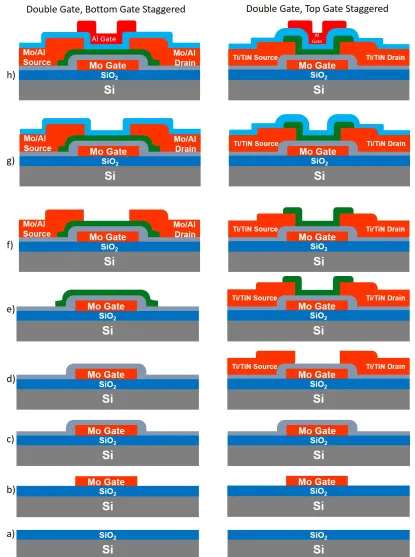
subtractive wet etch. A step by step illustration of the process flow as well as a
top-down micrograph and cross-sectional illustration can be seen in Fig. 3.3 and Fig. 3.4.
CHAPTER 3. SINGLE AND DOUBLE GATE TFTS
Figure 3.4: Fabrication results in a) double-gate from top gate on the left hand half and b) double-gate from bottom gate on the right hand half of the wafer. c) An optical microscope image of a double-gate with a staggered bottom gate IGZO TFT.
Table 3.1: Summary table of fabrication differences between each wafer. All wafers contain all possible device configurations.
Wafer Substrate Type Capping Layer Electrode Configuration
1 Silicon None All
2 Silicon 10 nm Al2O3 All
3 Glass None All
CHAPTER 3. SINGLE AND DOUBLE GATE TFTS
3.3
Bottom Gate TFTs
Figure 3.5: ID-VGStransfer characteristics of staggered bottom gate devices, with different
rest times.
TheID-VGS transfer characteristics for staggered bottom gate devices withW/L=
24/24µm and W/L = 24/12µm can be seen in Fig. 3.5. Upon testing these devices
exhibited a poor subthreshold slope and a 1 to 2 volt separation between low and
high drain characteristics. Subthreshold separation usually occurs for one of two
reasons, either the device was under-oxidized or over-oxidized during anneal. From
the results of previous research [13] it was determined that the devices were
over-oxidized rather than under-over-oxidized. For the process lot used in this study, the
only difference in fabrication was that the passivation TEOS was deposited 2-3 days
after IGZO deposition. In previous process lots, the passivation material generally
was not deposited until a week or two after IGZO deposition. Since remarkable
staggered bottom gate transfer characteristics were successfully realized with an eight
hour O2 anneal it is believed that a difference in the IGZO channel material caused
the over-oxidation. Mainly, it is suspected that the IGZO process lot in this study
was not given enough time to sit in room ambient before the passivation layer was
deposited. In order to test this hypothesis, passivated staggered bottom gate devices
After mesa and source/drain patterning the wafer was cleaved and half of the wafer
was annealed for 8-hours in an O2ambient. Directly after anneal, a 10 nm ALD Al2O3
film was deposited and contacts were patterned.
As per Fig. 3.5, devices that underwent an 8-hour O2 anneal and were delayed
for 2-months before passivation have a right-shifted VT and a superior subthreshold
slope. In comparison, devices that were delayed for 2-days before passivation are
severely distorted, displaying a left-shifted VT and subthreshold separation. From
this data, a hypothesis has been developed to explain this aging phenomenon. It is
believed that after deposition the IGZO film contains a high amount of interstitial
oxygen. As the film sits in a room ambient the oxygen is released into the air until
an equilibrium level is reached. As such, the longer the film sits in room ambient the
more oxygen is released. However, if a passivation material is deposited immediately
after IGZO deposition the interstitial oxygen is not allowed to release. As such, upon
introduction to an O2 anneal the film contains a super-saturated amount of oxygen
which results in an over-oxidation of the film if the anneal is too long, as shown in
Fig. 3.5.
This aging effect is thought to affect the electrostatics of the TFT back channel.
Therefore, an electrical comparison of bottom gate TFTs between each process
differ-ence was not able to be collected as all processed wafers appear to be compromised.
All other gate electrode configurations, however, appear to be able to compensate
for this effect and regain control over the IGZO back channel. This being the case a
statistical analysis and electrical comparison of all other gate-electrode configurations
was obtained. However, a definitive conclusion towards a superior gate-electrode
con-figuration and differences between processes cannot be made as these devices are most
CHAPTER 3. SINGLE AND DOUBLE GATE TFTS
3.4
Double Gate with Staggered Bottom Gate (DGBS) TFTs
3.4.1 Electrical Characteristics
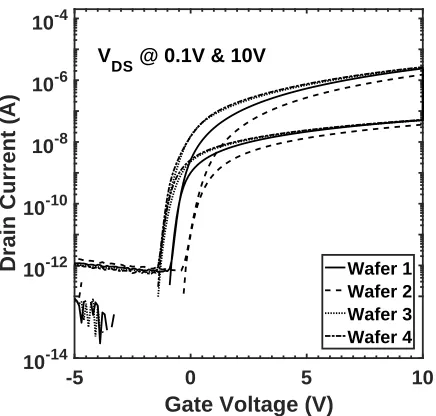
TheID-VGStransfer characteristics of double-gate with staggered bottom gate devices
on wafers 1−41outlined in Table 3.1 can be seen in Fig. 3.6. Representative extracted
parameters for the four treatments can be seen in Table 3.2. On silicon wafers with
an ALD capping layer a right shift inVT is observed along with a decline in mobility
and subthreshold slope. The opposite trend appears on the glass wafers for VT and
subthreshold slope. With an ALD capping layer, a left shift occurred in VT and the
subthreshold slope steepened on the glass wafer. One possibility for this reversal in
device behavior is that the gate dielectric thickness could be slightly different on the
glass wafers as compared to the silicon ones. Also, it must be noted that all device
parameters were extracted assuming the electrostatics of a single gate configuration
and the same oxide capacitance.
-5 0 5 10
Gate Voltage (V) 10-14
10-12 10-10 10-8 10-6 10-4
Drain Current (A)
V
DS @ 0.1V & 10V
[image:39.612.209.427.441.649.2]Wafer 1 Wafer 2 Wafer 3 Wafer 4
Figure 3.6: ID-VGS transfer characteristics ofW/L= 24/24µm double-gate from bottom
gate TFTs.
1Process differences on wafers as follows: W1-Si/No ALD, W2-Si/ALD, W3-Glass/No ALD,
Table 3.2: Extracted electrical characteristics of W/L= 24/24µm double-gate from bot-tom gate TFTs.
Wafer VT (V) σ (V) µ0 (cm2/Vs) σ (cm2/Vs) SS (mV/dec) σ (mV/dec)
1 0.2 0.2 14.35 1.24 267 48
2 1.1 0.3 12.92 1.98 354 77
3 −0.1 0.3 15.47 0.68 323 81
4 −0.6 0.2 13.64 1.02 229 74
Wafer 1 Wafer 2 Wafer 3 Wafer 4
Wafer # -1 -0.5 0 0.5 1 1.5 V TH (V)
Double Gate from Bottom Gate
Wafer 1 Wafer 2 Wafer 3 Wafer 4
Wafer # 11 12 13 14 15 16 17 18 µ eff (cm 2 /Vs)
Double Gate from Bottom Gate
Wafer 1 Wafer 2 Wafer 3 Wafer 4
Wafer # 200 300 400 500 SS (mv/dec)
Double Gate from Bottom Gate
CHAPTER 3. SINGLE AND DOUBLE GATE TFTS
To determine the behavior of the population of wafers 1−42a sample of 25 devices
were measured from each wafer. The notch of a boxplot represents the confidence
interval of the median. When the notches of separate boxplots overlap it can be
assumed with a 95% confidence level that the sample set is from the same population.
Since there are no overlapping notches, Fig. 3.7 shows that there are clear difference in
VT,µ0 and SS between each of these treatments. When considering device operation
wafer one shows a superior subthreshold slope and mobility; however, wafer three is
close runner up with a tight distribution in mobility.
3.4.2 Summary of Results DGBS
Silicon substrates show a right shift in threshold voltage but a decline in
subthresh-old slope with the inclusion of an ALD capping layer. Glass substrates, however,
show a left shift in threshold voltage and an improvement in subthreshold slope with
the inclusion of an ALD capping layer. Glass substrates also demonstrate a slight
improvement in mobility in comparison to silicon substrates.
2Process differences on wafers as follows: W1-Si/No ALD, W2-Si/ALD, W3-Glass/No ALD,
3.5
Double Gate with Staggered Top Gate (DGTS) TFTs
3.5.1 Electrical Characteristics
The ID-VGS transfer characteristics of double-gate with staggered top gate devices
on wafers 3 and 4 3 outlined in Table 3.1 can be seen in Fig. 3.8. Representative
extracted parameters for the two treatments can be seen in Table 3.3. Device results
are missing for the oxidized silicon substrates because of an error in fabrication that
resulted in the deposition of two source/drain regions for these devices. Ignoring noise
floor differences between the treatments it can be seen that an almost perfect overlay
exists between the two transfer curves. As shown in Fig. 3.3 the only difference
between the two treatments is a higher mobility for wafer three. It is believed that
the mobility would be similar if the series capacitance of the ALD capping layer was
considered. As such, it can be claimed that an ALD capping layer has little to no
effect on the transfer characteristics of a double-gate device with staggered top gate
and coplanar bottom gate configuration.
-5 0 5 10
Gate Voltage (V)
10-14 10-12 10-10 10-8 10-6 10-4
Drain Current (A)
V
DS @ 0.1V & 10V
[image:42.612.222.414.466.648.2]Wafer 3 Wafer 4
Figure 3.8: ID-VGS transfer characteristics ofW/L= 24/24µm double-gate from top gate
TFTs.
CHAPTER 3. SINGLE AND DOUBLE GATE TFTS
Table 3.3: Extracted electrical characteristics of W/L = 24/24µm double-gate from top gate TFTs.
Wafer VT (V) σ (V) µ0 (cm2/Vs) σ (cm2/Vs) SS (mV/dec) σ (mV/dec)
3 0.4 0.3 16.51 1.52 294 33
4 0.4 0.5 14.94 2.32 296 37
Wafer 3 Wafer 4
Wafer # -0.5 0 0.5 1 V TH (V)
Double Gate from Top Gate
Wafer 3 Wafer 4
Wafer # 8 10 12 14 16 18 µ eff (cm 2 /Vs)
Double Gate from Top Gate
Wafer 3 Wafer 4
Wafer # 220 240 260 280 300 320 340 360 SS (mv/dec)
Double Gate from Top Gate
To determine the behavior of the population of wafers three and four 4, a sample
of 25 devices were measured from wafer three. Due to a yield issue on the wafer only
a sample of 15 devices was able to be measured on wafer four. It is believed that this
issue was caused by non-uniformity during the dielectric deposition step. As a result,
the true median of the devices is not able to be determined with a 95% confidence
level. In Fig. 3.9 this is represented by a notch going beyond the interquartile range.
Even with this issue, however, it can be seen that an overlap occurs for VT and
subthreshold slope, which means that the sample sets are possibly from the same
population. To truly determine if the sample sets are similar a larger sample size is
needed.
3.5.2 Summary of Results DGTS
For both treatments on the glass substrates no difference can be observed between
the transfer curves. In the transfer characteristics a decline in mobility can be seen
for the ALD capping layer treatment. However, it is believed that the mobility would
be similar if the series capacitance of the ALD capping layer was considered when
extracting parameters.
CHAPTER 3. SINGLE AND DOUBLE GATE TFTS
3.6
Staggered Top Gate (TGS) TFTs
3.6.1 Electrical Characteristics
The ID-VGS transfer characteristics of staggered top gate devices on wafers 3 −4 5
outlined in Table 3.1 can be seen in Fig. 3.10. Representative extracted parameters for
the four treatments can be seen in Table 3.4. As with the double-gate with staggered
top gate devices results are missing for the oxidized silicon substrates because of an
error in fabrication that resulted in the deposition of two source/drain regions for
these devices. The device from wafer three shows a right shifted curve and little to
no separation between low and high drain curves. The wafer three device also shows
a superior subthreshold slope however, the current drive of both devices is identical.
As such, it the device on wafer four displays weaker control over defect states and the
channel than that on wafer three.
-5 0 5 10
Gate Voltage (V)
10-14 10-12 10-10 10-8 10-6 10-4
Drain Current (A)
V
DS @ 0.1V & 10V
[image:45.612.197.435.416.644.2]Wafer 3 Wafer 4
Figure 3.10: ID-VGStransfer characteristics ofW/L= 24/24µm staggered top gate TFTs.
Table 3.4: Extracted electrical characteristics of W/L = 24/24µm staggered top gate TFTs.
Wafer VT (V) σ (V) µ0 (cm2/Vs) σ (cm2/Vs) SS (mV/dec) σ (mV/dec)
3 0.5 0.5 9.60 0.32 398 25
4 −0.1 0.1 9.45 0.40 502 98
Wafer 3 Wafer 4
Wafer # -1.5 -1 -0.5 0 0.5 1 V TH (V)
Staggered Top Gate
Wafer 3 Wafer 4
Wafer # 8.8 9 9.2 9.4 9.6 9.8 10 10.2 µ eff (cm 2 /Vs)
Staggered Top Gate
Wafer 3 Wafer 4
Wafer # 350 400 450 500 550 600 650 700 SS (mv/dec)
Staggered Top Gate
CHAPTER 3. SINGLE AND DOUBLE GATE TFTS
To determine the behavior of the population of wafers 3 and 4 6 a sample of 25
devices were measured from each wafer. As with the double-gate with staggered top
gate devices a smaller sample set, 10 devices, was obtained for wafer four because of
a yield issue. As such, the true medians of the wafer four device characteristics are
not able to be determined with a 95% confidence level. If the region of the notch
beyond the interquartile range is considered invalid then only the mobility of the
two samples overlap. From transfer characteristics alone, a glass substrate without
an ALD encapsulation layer can be considered superior for the staggered top gate
configuration.
3.6.2 Summary of Results T GS
Characteristics for the silicon substrates were not extracted due to a fabrication issue
that resulted in two source/drain regions for these devices. On the glass substrates, a
steeper subthreshold is observed for the no-ALD barrier treatment. The characteristic
of wafer four seems to lend itself to a different distribution of trap states in the channel.
This is believed to cause the spreading out and separation in the transfer curve.
3.7
Coplanar Top Gate (TGC) TFTs
3.7.1 Electrical Characteristics
The ID-VGS transfer characteristics of coplanar top gate devices on wafers 1 −4 7
outlined in Table 3.1 can be seen in Fig. 3.12. Representative extracted parameters
for the four treatments can be seen in Table 3.5. While all the treatments show
reasonable off-state characteristics the subthreshold and on-state operation is a bit
challenged. For starters, all treatments show a suboptimal average subthreshold slope.
Also wafer three shows a separation between the low and high drain characteristics
while wafer one shows a hysteresis-like effect. While wafers 2 and 4 don’t show
separation between the low and high drain curves their current drive is slightly less
than that of wafers 1 and 3. The lower current drive of coplanar top gate devices
is the result of thicker oxide near the edge of the channel due to the topology of
the metal S/D regions. The lowered capacitance in these areas makes it difficult to
control the channel where this topology occurs.
-5 0 5 10
Gate Voltage (V)
10-14 10-12 10-10 10-8 10-6 10-4
Drain Current (A)
V
DS @ 0.1V & 10V
[image:48.612.221.414.466.654.2]Wafer 1 Wafer 2 Wafer 3 Wafer 4
Figure 3.12: ID-VGStransfer characteristics ofW/L= 24/24µm coplanar top gate TFTs.
7Process differences on wafers as follows: W1-Si/No ALD, W2-Si/ALD, W3-Glass/No ALD,
CHAPTER 3. SINGLE AND DOUBLE GATE TFTS
Table 3.5: Extracted electrical characteristics ofW/L= 24/24µm coplanar top gate TFTs.
Wafer VT (V) σ (V) µ0 (cm2/Vs) σ (cm2/Vs) SS (mV/dec) σ (mV/dec)
1 0.3 1.0 4.86 1.72 404 73
2 0.6 1.1 4.77 2.51 544 209
3 −1.3 1.2 2.08 1.58 404 57
4 −0.5 1.4 3.06 1.53 329 59
Wafer 1 Wafer 2 Wafer 3 Wafer 4
Wafer # -4 -3 -2 -1 0 1 2 V TH (V)
Coplanar Top Gate
Wafer 1 Wafer 2 Wafer 3 Wafer 4
Wafer # 2 4 6 8 10 µ eff (cm 2 /Vs)
Coplanar Top Gate
Wafer 1 Wafer 2 Wafer 3 Wafer 4
Wafer # 400 600 800 1000 1200 SS (mv/dec)
Coplanar Top Gate
To determine the behavior of the population of wafers 1− 4 8 a sample of 25
devices were measured from each wafer. As can be seen in Fig. 3.13 the coplanar
top-gate configuration appears inferior to other electrode configurations. Each treatment
appears to have a wide spread on all device characteristics. To truly determine if the
sample sets are similar and to get more defined distribution a larger sample size is
required.
3.7.2 Summary of Results T GC
While the coplanar top gate configuration is the easiest and quickest to fabricate the
low quality electrical characteristics outweigh the efficiency gains. For all process
modifications a low mobility and high subthreshold swing is observed. Also, when
devices were fabricated on glass the electrical performance was degraded. These
devices also presented a lower current drive as a result of thicker oxide near the edge
of the channel due to the topology of the metal S/D regions. The lowered capacitance
in these areas makes it difficult to control the channel where this topology occurs.
8Process differences on wafers as follows: W1-Si/No ALD, W2-Si/ALD, W3-Glass/No ALD,
CHAPTER 3. SINGLE AND DOUBLE GATE TFTS
3.8
Evaluation of Electrode Configurations
This section presents a quantitative analysis of DGBS, DGTS, T Gcop, and T Gstg
configurations with a glass substrate and an ALD capping layer. An overlay of ID
-VGS transfer characteristics can be seen in Fig. 3.14. It is important to note that the
coplanar top gate configuration has a max current roughly one order of magnitude
less than the other configurations This is thought to be the result of thicker oxide
near the edge of the channel due to the topology of the metal S/D regions. The
lowered capacitance in these areas makes it difficult to control the channel where this
topology occurs.maximum current roughly one order of magnitude less than the other
configurations.
-5 0 5 10
Gate Voltage (V)
10-14 10-12 10-10 10-8 10-6 10-4
Drain Current (A)
V
DS @ 0.1V & 10V
Double Gate with Staggered Bottom Double Gate with Staggered Top Staggered Top Gate
[image:51.612.199.435.360.586.2]Coplanar Top Gate
Figure 3.14: ID-VGS transfer characteristics of W/L = 24/24µm devices with a glass
substrate and ALD capping layer.
To further quantify the difference in these configurations box plots were generated
in Fig. 3.15. The sample size of all device configurations was 25. There is a noted
improvement in µ0 when going from a top-gate configuration to either double-gate
value consistent with a single-gate. Due to its improved subthreshold performance the
double-gate with a staggered top gate could be the optimal electrode configuration;
however, a larger sample size is required to make a definitive conclusion.
DGTS DGBS TGC TGS
Device Configuration -4 -3 -2 -1 0 1 2 V TH (V)
DGTS DGBS TGC TGS
Device Configuration 5 10 15 µ eff (cm 2 /Vs)
DGTS DGBS TGC TGS
[image:52.612.123.513.171.537.2]Device Configuration 250 300 350 400 450 500 550 SS (mv/dec)
Figure 3.15: Extracted parameters from W/L=24/24µm devices with a glass substrate and ALD capping layer.
3.8.1 Bias Stress Stability
The bias-stress stability of TFTs is an important parameter when considering the
lifetime of a display. Over time bias-stress can lead to VT shifts which affect the
display brightness and may eventually result in sub-pixels not turning either on or
CHAPTER 3. SINGLE AND DOUBLE GATE TFTS
but only devices fabricated on a glass substrate will be evaluated. The TFT
chan-nel dimensions are W/L = 24/24µm. An initial measurement was performed, then
devices were put under stress according to the conditions listed in Table 3.6.
Imme-diately following the stress the devices were measured again. These ID-VGS transfer
[image:53.612.140.514.250.691.2]characteristics can be seen in Figs. 3.16–3.19.
Table 3.6: Bias stress conditions.
Parameter Value
VGS (V) ±10
VDS (V) 0
VSS (V) 0
Stress Time (min) 60
Figure 3.16: Negative (right) and positive (left) bias stress response for devices of W/L
As seen in Fig. 3.16 the double-gate with a staggered bottom gate on wafer 3
shows moderate instability after both negative bias stress (NBS) and positive bias
stress (PBS). Notably, a parallel left shift is seen after NBS and a parallel right shift
is seen after PBS. On the other hand wafer four showed a very slight parallel left
shift after PBS and no shift after NBS. Due to a lack of sampling it is impossible to
conclude if an ALD capping layer really improves bias stress stability or if this is an
[image:54.612.138.512.257.566.2]anomaly.
Figure 3.17: Negative (right) and positive (left) bias stress response for devices of W/L
= 24/24µm for DGTS configuration of wafer three and four.
As seen in Fig. 3.17 the double-gate with a staggered top gate on wafer 3 shows
significant instability after PBS. Notably, a parallel right shift is observed after PBS.
Stability was better with NBS with no discernible shift observed after one hour under
CHAPTER 3. SINGLE AND DOUBLE GATE TFTS
under both bias conditions. For both NBS and PBS no discernible shift was observed
after one hour under stress. Much like the double-gate with a staggered bottom
gate configuration, additional sampling is required to conclude that an ALD barrier
[image:55.612.139.513.184.490.2]improves bias stress stability.
Figure 3.18: Negative (right) and positive (left) bias stress response for devices of W/L
= 24/24µm for TGS configuration of wafer three and four.
For wafer three the staggered top gate configuration behaves much like its
re-spective double-gate configuration, as can be seen in Fig. 3.18. No discernible shift
was observed after one hour under NBS and a significant right shift, ≈3 volts, was
observed after one hour under PBS. On the other hand, wafer four showed a
signif-icant left shift after PBS. Interestingly, an improvement in subthreshold slope and
separation can be seen after PBS. However, due to lack of sampling it is unknown if
this is an anomaly. Much like wafer three no discernible shift was observed after one
Figure 3.19: Negative (right) and positive (left) bias stress response for devices of W/L
= 24/24µm for TGC configuration of wafer three and four.
For wafer three the coplanar top gate shows significant instability after PBS, as can
be seen in Fig. 3.19. Notably, a parallel right shift and slight subthreshold separation
is seen after PBS. Stability was better after NBS with only a slight left shift being
observed. After PBS, wafer four showed the same amount of subthreshold separation
but not as significant of a right shift as wafer 3. Under NBS however, no shift in the
transfer curve can be seen. Instead, a large subthreshold separation and degradation
CHAPTER 3. SINGLE AND DOUBLE GATE TFTS
3.9
Summary of Single and Double Gate TFTs
A new photomask was created that enables the fabrication of all gate configurations
within each test chip. Using the proces flow outlined in Sec. 3.2 all possible device
configurations were fabricated on glass and oxidized silicon substrates. In order to
determine if an ALD capping layer affects device electrical characteristics one of
each substrate type was fabricated without ALD Al2O3 on top of the TEOS layers.
Transfer characteristics for each configuration were then extracted and compared.
Due to a possible IGZO aging phenomena all devices experienced an over-oxidizing
anneal. As such, the staggered bottom gate devices displayed a degraded subthreshold
slope and a one volt separation between the low and high drain characteristics. This
aging effect is hypothesized to be the result of interstitial oxygen being released from
the IGZO material into room ambient.
Compared to the other device configurations both double-gate configurations show
an improved subthreshold slope, a right-shifted VT, and an improvement in mobility.
It was also observed that an ALD capping layer has little to no effect on the electrical
performance of double-gate configurations. The staggered top gate configuration
was superior to the coplanar top gate which suffered from low current drive, poor
subthreshold slope, and degraded mobility. The single gate configurations showed a
discernible difference between devices with and without an ALD capping layer. This,
however, may be a consequence of the devices being over-oxidized.
More lateral shifting is observed in the single gate configurations under positive
bias stress. For the double-gate configurations no discernible shift is observed under
both positive and negative bias stress when an ALD capping layer is present in the
de-vice structure. This may show that an ALD capping layer is useful for the suppression
of bias stress instabilities; however, as previously stated this may be a consequence
indicate that the double-gate with a staggered top gate configuration is superior for
transfer characteristics and bias stress susceptibility. Variants on source/drain to gate
overlap were not bias stress tested as the results would not be conclusive, due to the
[image:58.612.109.541.244.447.2]device compromise. A qualitative summary of all electrical results can be seen in
Table 3.7.
Table 3.7: A qualitative summary of all electrical tests carried out on all electrode config-urations.
Transfer Characteristics
DGBS TGC DGTS TGS
Oxidized Si Glass Oxidized Si Glass Glass Glass
VT Good Ok Good Bad Good Ok
µ0 Good Good Bad Bad Good Ok
SS Good Good Bad Bad Good Bad
Bias Stress Response
DGBS TGC DGTS TGS
ALD No ALD ALD No ALD ALD No ALD ALD No ALD PBS Good Bad Ok Bad Good Bad Bad Ok
NBS Good Bad Ok Ok Good Good Good Good
These results are promising and future work will include larger sampling and more
aggressive bias stress testing as well as determining the effect of source/drain to gate
overlap on bias stress susceptibility. These results indicate that the condition of the
secondary interface, which is exposed to processing after the IGZO sputter, is critical
to the final electrical performance of IGZO TFTs. Further understanding of what is
occurring at this interface is required to refine the scope of future research into IGZO
Chapter 4
Comprehensive Device Model
4.1
Motivation
The development of a consistent and reliable parameter extraction model is of
para-mount importance if a quantitative analysis and comparison of different treatments
is required. It is important for this method to add minimum error so that any
dif-ferences observed can be accounted for by processing difdif-ferences. IGZO TFTs do
not show normal field degradation when operated in linear mode as silicon devices
do as shown in Fig. 4.1. Thus, traditional methods used for silicon devices, such as
extracting VGS at the maximum transconductance for VT do not work. An attempt
to use this method will result in a grossly overestimated VT and subsequently µT H
and µ0. Traditional methods used for IGZO TFTs calculate VT at the maximum of
the derivative of gm. This method provides an acceptable, albeit conservative
mea-surement of VT; however, this is not a robust method when attempts are made to
1 2 3 4 5
Gate Voltage (V)
0.5 1 1.5 2 2.5 3 3.5 4
Drain Current (A)
×10-5
0 2 4 6 8 10
Gate Voltage (V)
0 0.5 1 1.5 2
Drain Current (A)
×10-6
Figure 4.1: LinearID-VGS measurements of a-SI:H (left) and IGZO (right) TFTs.
4.2
Refinement of Spice Level 2 Model
4.2.1 Initial Model Shortcoming
Even though a good match exists between the measured and modeled data, the
original device model was far from perfect. When attempting to model the family
of curves an issue arose where the model could accurately predict the initial and
saturation currents but nothing else, as shown in Fig. 4.2. In the initial model an
effective channel mobility model was used, as shown in Eq. 4.1.
µef f =
µch
1 + (VGS−VTlin)θ
(4.1)
This approximation is appropriate if the carrier mean free path is on the order of
the chemical bond length. In the case of IGZO however, the electron mean free
path is significantly larger than the inter
![Figure 1.2: Mobility requirements for current and future displays [1].](https://thumb-us.123doks.com/thumbv2/123dok_us/73856.6951/18.612.174.476.233.466/figure-mobility-requirements-current-future-displays.webp)
![Figure 1.3: Active matrix VT compensation circuit utilizing 4 TFTs and 2 storage capac-itors [5].](https://thumb-us.123doks.com/thumbv2/123dok_us/73856.6951/19.612.219.432.183.398/figure-active-matrix-compensation-circuit-utilizing-tfts-storage.webp)