UNIVERSITI TEKNIKAL MALAYSIA MELAKA
DEVELOPMENT OF FPGA BASED PORTABLE LOW-COST
DIGITAL SIGNAL GENERATOR
This report is submitted in accordance with the requirement of Universiti Teknikal Malaysia Melaka (UTeM) for the Bachelor of Computer Engineering Technology
(Computer System) with Honours
by
IRNA NADIRA BINTI MAHZAN B071410460
950612-04-5058
UNIVERSITI TEKNIKAL MALAYSIA MELAKA
BORANG PENGESAHAN STATUS LAPORAN PROJEK SARJANA MUDA
TAJUK: DEVELOPMENT OF FPGA BASED PORTABLE LOW-COST DIGITAL SIGNAL GENERATOR
SESI PENGAJIAN: 2017/2018 Semester 1
Saya IRNA NADIRA BINTI MAHZAN
mengaku membenarkan Laporan PSM ini disimpan di Perpustakaan Universiti Teknikal Malaysia Melaka (UTeM) dengan syarat-syarat kegunaan seperti berikut: 1. Laporan PSM adalah hak milik Universiti Teknikal Malaysia Melaka dan penulis. 2. Perpustakaan Universiti Teknikal Malaysia Melaka dibenarkan membuat salinan
untuk tujuan pengajian sahaja dengan izin penulis.
3. Perpustakaan dibenarkan membuat salinan laporan PSM ini sebagai bahan pertukaran antara institusi pengajian tinggi.
4. **Sila tandakan ( )
SULIT
TERHAD
/ TIDAK TERHAD
(Mengandungi maklumat yang berdarjah keselamatan atau kepentingan Malaysia sebagaimana yang termaktub dalam AKTA RAHSIA RASMI 1972)
(Mengandungi maklumat TERHAD yang telah ditentukan oleh organisasi/badan di mana penyelidikan dijalankan)
Alamat Tetap: No 18, Tembusu 8, Taman Merdeka,
75350 Batu Berendam, Melaka.
Tarikh: ________________________
Disahkan oleh:
Cop Rasmi:
iii
DECLARATION
I hereby, declared this report entitled “Development Of FPGA Based Portable Low-Cost Digital Signal Generator” is the result of my own research except as cited in
references.
iv
APPROVAL
This report is submitted to the Faculty of Engineering Technology of UTeM as a partial fulfilment of the requirements for the Bachelor's Degree of Computer Engineering Technology (Computer System) with Honours. The members of the supervisory committee are as follow:
………. (Encik Aiman Zakwan bin Jidin)
v
ABSTRACT
vi
ABSTRAK
Penjana Isyarat adalah alat yang menjana bentuk gelombang voltan berulang yang penting untuk menjana kawalan frekuensi dan amplitud yang tepat.Penjana isyarat juga mempunyai melengkapkan mikropengawal (CPU) yang boleh digunakan pada mana-mana sistem ujian dengan surat cara lain atau dikawal oleh komputer. Walau bagaimanapun, sebahagian besar daripada penjana isyarat komersial adalah sangat mahal. Harga bagi setiap penjana isyarat adalah kira-kira RM1 500 - RM 20 000. Saiz penjana isyarat juga besar dan berat menyebabkan ia sukar untuk menjalankan mana-mana. Oleh itu, tujuan projek ini adalah untuk membangunkan kos
rendah mudah alih penjana isyarat digital dengan menggunakan Field Programmable
Gate Array (FPGA). Cadangan projek yang dinyatakan di dalam High Discription
Language (HDL) dan huraian disahkan dengan menggunakan Altera Quartus Software
Design Interface dan ModelSim. Selepas kod rekabentuk yang disahkan oleh
ModelSim, reka bentuk akan dilaksanakan di papan FPGA dan SignalTap sebagai
Logik Analyzer akan menjana isyarat. Berdasarkan keputusan dari SignalTap, analisis
vii
DEDICATIONS
Alhamdulillah..
Thank Allah because of His grace, I have been able to prepare this project successfully. Appreciation to my beloved parents, En Mahzan Bin Paiman and Pn. Habibah Binti Said. I acknowledge my sincere indebtedness and gratitude to them for their love, dream and sacrifice throughout my life. I am really thankful for their sacrifice, patience, giving spirit and strength to me in a life filled with these allegations.
viii
ACKNOWLEDGMENTS
First and foremost, all praise to Allah the Almighty for giving me the strength, health, knowledge and patience to successfully complete this Finale Year Project report at the given time. I have to thank my parents for their love and support throughout my life.I would like to address my deepest appreciation to the supervisor, Encik Aiman Zakwan bin Jidin and to the co-supervisor, Encik Noor Mohd Ariff bin Brahin who provide encouragement, comments guidance and advice to me in conducting research and writing report.
ix
TABLE OF CONTENT
DECLARATION………….………...iii
APPROVAL………...iv
ABSTRACT………...……v
ABSTRAK……….…vi
DEDICATION………...vii
ACKNOWLEDGEMENT……….viii
TABLE OF CONTENT……….…ix
LIST OF TABLE………...xiii
LIST OF FIGURE……….…xiv
LIST OF SYMBOL, ABBREVIATIONS AND NOMENCLATURE……….xvii
CHAPTER 1: INTRODUCTION……….1
1.0 Introduction………..1
1.1 Background………..1
1.2 Problem Statement………...3
1.3 Objective……….……….4
1.4 Scope of Work……….4
1.5 Project Significant………...5
1.6 Outline……….5
CHAPTER 2: LITERATURE REVIEW……….………7
2.0 Introduction……….……….7
x
2.1.1 Function Generator ……….7
2.1.2 Arbitrary Waveform Generators…..……….…………...9
2.1.3 RF Signal Generators ………..………...10
2.1.3.1 Analog Signal Generators………...11
2.1.3.2 Vector Signal Generators ………11
2.1.3.3 Logical Signal Generators………...11
2.1.4 Audio Signal Generator….………..11
2.2 Signal Generation Method………..12
2.2.1 Sine Wave ………...12
2.2.2 Square Wave ………...13
2.2.3 Triangular Wave………..14
2.3 Previous Work………15
2.3.1 FPGA-Based Function Generator ………..15
2.3.2 Waveform Generator Implemented in FPGA with an Embedded Processor……….16
2.3.3 Comparison between Previous Project and Proposed Project ………17
2.4 Theory of Component ………...19
2.4.1 Hardware ………19
2.4.1.1.Altera DE0 FPGA Board………19
2.4.1.2 FPGA vs. Embedded System………...21
2.4.2 Software………..22
2.4.2.1 HDL coding……….22
2.4.2.2 Altera Quartus II Design Software………..23
xi
2.4.2.4 Signal Tap………...24
CHAPTER 3: METHODOLOGY………..25
3.0 Introduction ………...25
3.1 Project Execution Flow ……….25
3.2 Project Overview ………...28
3.2.1 Functionality/Operation Flowchart ………...29
3.2.2 Insert Frequency Flowchart……….30
3.3 Hardware Development Using Verilog………..32
3.3.1 Sine Wave………...32
3.3.2 Triangular Wave………...33
3.3.4 Square Wave………...34
3.4 Design and Preparation of the System ………34
3.4.1 Material and Equipment………..35
3.5 Budget and Costing ………....38
3.5.1 Direct Cost ………..38
3.2.2 Software Cost………..39
CHAPTER 4: RESULT & DISCUSSION………..40
4.0 Introduction ……….40
4.1 Project Implementation………40
4.2 Simulation Result………..44
4.2.1 Sine Wave……….44
4.2.2 Triangular Wave………..47
4.2.3 Pulse/Square Wave………..50
xii
4.4 Hardware Experiment Test setup………..55
4.5 Hardware Result in Signal Tap……….56
4.5.1 Sine Wave……….57
4.5.2 Triangular Wave………...58
4.5.3 Square Wave……….60
4.6 Discussion……….61
4.7 Project Limitation……….63
CHAPTER 5: CONCLUSION & FUTURE WORK………...64
5.0 Introduction………...64
5.1 Expected Result……….64
5.2 Recommendation………...65
5.3 Commercialization Potential………...65
REFERENCES………...66
APPENDIX………....68
A. Sine_Memory 68
B. TriangleWave 73
C. SquareWave 74
D. function_generator 75
E. fsm_controller 78
F. RS232 81
xiii
LIST OF TABLES
2.1 Comparison between Previous Project with Proposed Project………..19
3.1 List of Material and Equipment ………35
3.2 Direct Cost……….38
3.3 Software Cost……….39
4.1 Measured Frequency Vs Desired Frequency for Sine Wave……….47
4.2 Measured Frequency Vs Desired Frequency for Triangular Wave………...50
4.3 Measured Frequency Vs Desired Frequency for Square Wave………..53
4.4 Measured Frequency Vs Desired Frequency of Sine Wave………...58
4.5 Measured Frequency Vs Desired Frequency for Triangular Wave…………69
xiv
LIST OF FIGURES
1.1 Function Generator ………2
1.2 Basic Signal Waveform ……….3
2.1 Block Diagram of Function Generator ………..9
2.2 Arbitrary Waveform Generator ……….10
2.3 A Staircase Sine Wave Approximation …………...………..13
2.4 Square Wave……….…..14
2.5 Generator Triangular wave from a Square Wave………..….14
2.6 Block Diagram from FPGA-Based Function Generator Project………15
2.7 Block Diagram Previous Project of Waveform Generator ………....17
2.8 Comparison Altera and Xilinx ………...18
2.9 Cyclone III FPGA Starter Board ………21
3.1 Project Flowchart ………...…………27
3.2 Block Diagram of the project ………...28
3.3 Choose Signal Flowchart ………...30
3.4 Insert Frequency Flowchart ………...31
3.5 System Architecture for Sine Wave………33
3.6 The Triangular Wave Verilog code………....34
3.7 The Square Wave Verilog code………...34
4.1 Circuit of System Architecture Signal Generator………..41
4.2 Sine Wave Circuit ………...41
xv
4.4 Square Wave Circuit…...………...43
4.5 Hardware Resources of Usage Statistic……….43
4.6 Sine Waveform with 1kHz frequency………...45
4.7 Sine Waveform with 5kHz frequency ………...45
4.8 Sine Waveform with 10kHz frequency ………...45
4.9 Sine Waveform with 77kHz frequency ……….46
4.10 Sine Waveform with 313kHz frequency ………...46
4.11 Sine Waveform with 1MHz frequency ………46
4.12 Triangular Waveform with 1kHz frequency ………48
4.13 Triangular Waveform with 5kHz frequency ………48
4.14 Triangular Waveform with 10kHz frequency ………..48
4.15 Triangular Waveform with 77kHz frequency ………..49
4.16 Triangular Waveform with 313kHz frequency ………49
4.17 Triangular Waveform with 1MHz frequency ………...49
4.18 Square Waveform with 1kHz frequency ………51
4.19 Square Waveform with 5kHz frequency ………51
4.20 Square Waveform with 10kHz frequency ………..51
4.21 Square Waveform with 77kHz frequency ………...52
4.22 Square Waveform with 313kHz frequency ……….52
4.23 Square Waveform with 1MHz frequency ………...…………52
4.24 Part of code which is DropdownList ………..53
xvi
4.26 The six 8-bit word ………...54
4.27 Data transmitted for the Triangular Wave with 667 KHz ………...55
4.28 Hardware Setup ………...55
4.29 The System Architecture of Signal Generator ………56
4.30 Sine Wave Output with 100kHz Frequency ………..57
4.31 Sine Wave Output with 250kHz Frequency ………...57
4.32 Sine Wave Output with 667kHz Frequency ………...58
4.33 Triangular Wave Output with 100kHz Frequency ……….59
4.34 Triangular Wave Output with 250kHz Frequency ……….59
4.35 Triangular Wave Output with 667kHz Frequency ……….59
4.36 Square Wave Output with 100kHz Frequency ………...60
4.37 Square Wave Output with 250kHz Frequency ………...60
4.38 Square Wave Output with 667kHz Frequency ………...60
4.39 Stair step for Each Sample ………...62
xvii
LIST OF SYMBOLS, ABBREVIATIONS AND
NOMENCLATURE
FPGA - Field Programmable Gate Array HDL - High Digital Language
CPU - Control Processor Unit RF - Radio Frequency AM - Amplitude Modulation FM - Frequency Modulation FSK - Frequency-shift Keying DDS - Direct Digital Synthesizer DAC - Digital Analog Converter
UART - Universal Asynchronous Receiver/Transmitter DSC - Digital Signal Controllers
1
CHAPTER 1
INTRODUCTION
1.0 Introduction
This chapter explains the background of this project, problem statement, objectives, work scope, project significant and conclusion. The structure of this report of the project is briefly explained to ensure a better visualization of the sequence of the entire project.
1.1 Background
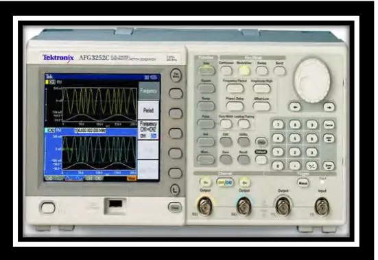
The signal generator is a device that generates repeating voltage waveforms. It is important device to find a wide range of applications in the electronic laboratory. Most of all signal generator is used to generate the signal with accurate controlled frequency and amplitudes. Besides, the signal generator can generate a high frequency to provide high-frequency resolution. It is used for designing, testing and troubleshooting electronic devices. Besides, the signal generator also can be used on any test system with other instrument or to be controlled by the computer.
2
[image:19.595.183.459.360.550.2]align all types of transmitters and receivers, to measure frequency, and to generate a signal, waveform, or noise source. Signal generators can use AC energy, audio frequency (AF), and radio frequency (RF) to function. They are also used to troubleshoot various electronic devices and to measure frequency. The function of a signal generator is to produce alternating current (AC) of the desired frequencies and amplitudes with the necessary modulation for testing or measuring circuits. It is important that the amplitude of the signal generated by the signal generator be correct. In many signal generators, output meters are included in the equipment to adjust and maintain the output at standard levels over wide ranges of frequencies. When using the signal generator, the output test signal is connected to the circuit being tested. The progress of the test signal can then be tracked through the equipment by using electronic voltmeters or oscilloscopes.
3
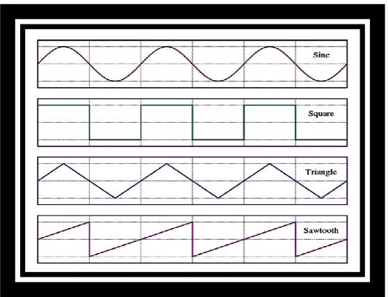
Figure 1.2: Basic Signal Waveform
1.2 Problem Statement
The signal generator is the device that is important in many communication and other signal related applications. It is widely used in an experimental course in UTeM. The signal generator is used to get generate square wave, sine wave and triangle wave signal. It is usually as a standard signal in electronic circuit testing, parameter measurement, or demonstration in the experimental course.
However, most of the signal generator is too expensive. UTeM known as technical universities are really needed many of this device for the lab session. Therefore, the universities need to spend high budget for buy this device. The result is limited working mode and cannot be played entirely in the teaching experiments of a common signal generator.
4
Furthermore, most of commercial low-cost function generator are limited in term of frequency and amplitude variation. It provides a very small range of frequency and amplitude of the signal. Therefore, the purpose of this project is to develop a small-sized and highly accurate economic digital signal generator by using FPGA which can provide wave signals commonly used in experiments.
1.3 Objective
The objectives of this project are:
1. To study about basic digital signal generation method.
2. To develop a portable behaviour low-cost digital signal generator by using FPGA.
3. To interface Graphical User Interface(GUI) for signal configuration. 4. To analyse the overall performance and the reliability of the system.
1.4 Scope of Work
In order to obtain a clearer visualisation and to achieve the objective for this project, the scope of this project has optimised. This current project consisting of two work scope. First work scope is about hardware which is Field-Programmable Gate Array (FPGA). FPGA device will be used in this project. It is a programmable IC which has highest integration and complexity. The function of FPGA is to install the Altera design and generate basic signal generation such as Sine, Pulse and Triangle signal. Using USB cable, the FPGA will be connected to the computer.
5
This project is using GUI application for choosing the type of signal and frequency value. The software to design GUI is using Processing Software. Then, SignalTap will display the desired frequency of the basic signal generation. The function of SignalTap is it can be used to capture and display signal in real time in any FPGA design.
After the signal is displayed, test analysis will be carried out. The frequency is correctly proving by doing the mathematical operation and compared to the frequency output signal on SignalTap as a Logic Analyzer. Logic Analyzer displays signal in a digital circuit that to observe and presents which can be more easily check the operation of the digital system with precision. The signal should have an output data rate at is condition 1 kHz- 1 MHz. It provides a clear and precise window into the frequency spectrum measuring all of the signals with more accurate measurements and interpreting the result correctly.
1.5 Project Significant
This project is contributed to universities or students which need to do experiments which generate the basic signal and not too high-frequency waveform. Besides, this project is not too expensive and it is affordable for students, researchers or average user to buy and have their own signal generator. The size of this project signal generator also small and easy to carry anywhere. It also has a higher performance of the portable digital signal generator. Furthermore, it is reusable because it can be generated or use many times.
1.6 Outline
6
7
CHAPTER 2
LITERATURE REVIEW
2.0 Introduction
A literature review is a previous study in the form of the reference book, articles, journals and the internet that used to refer, taking ideas from previous has or studies in order to improve future use. All of the sources have a very useful information that guides in doing this project. Each review sources are selected according to the similarity of project's scope.
2.1 Types of Signal Generator
There are different types of signal generators with different capability and functionality. All the signal generators have different designs, dimensions and parameters. Therefore, there have different purposes and cover a range of applications. Every versatile signal generators can create an unlimited number of the signal to meet the debug challenges.
2.1.1 Function Generator