Int. J. Electrochem. Sci., 9 (2014) 7865 - 7874
International Journal of
ELECTROCHEMICAL
SCIENCE
www.electrochemsci.orgEffect of Double Layer (SiO
2/TiO
2) Anti-reflective Coating on
Silicon Solar Cells
Khuram Ali*, Sohail A. Khan, M. Z. Mat Jafri
Nano-Optoelectronics Research and Technology Laboratory, School of Physics, Universiti Sains Malaysia, Penang 11800, Malaysia
*
E-mail: [email protected]
Received: 18 August 2014 / Accepted: 9 September 2014 / Published: 28 October 2014
Silicon based solar cells have been fabricated for single layer SiO2 and double layer SiO2/TiO2 antireflective coatings (ARC) using rf sputtering technique. The results were obtained with non-texturized surface of p-type mono-crystalline silicon (100) substrate and compared with the as-grown Si solar cell. Effect of single layer (SLAR) and double layer (DLAR) AR coatings on the performance of solar cell were characterized through electrical (AM 1.5G, 100 mW/cm2), optical and morphological measurements. The addition of the DLAR initiated 37% improvement in the efficiency of the mono-crystalline Si solar cells, compared with 4.5% of the SLAR Si solar cell. Morphological and optical measurements were carried out by atomic force microscopy (AFM), field emission scanning electron microscopy (FESEM), Raman spectra and reflectance spectra. A reflection spectrum of DLAR was also measured which shows the minimum reflection of 2.3% at 630 nm with an average reflection of 7% (within the 400-1000 nm range). The results indicated that the DLAR SiO2/TiO2 coatings could be valuable in achieving highly absorbent surfaces in optoelectronic devices as well as in the production of high efficiency low cost silicon solar cells.
Keywords: double layer anti reflection coating; silicon solar cell, sputtering, SiO2/TiO2
1. INTRODUCTION
get low solar cell reflectance. To achieve lowest reflection of a single wavelength of incident radiation, the ARC may consist of a SLAR, which must retain (a) square root of the refractive indices of the materials constrained the coating equal to the refractive index of the ARC and (b) thickness of ARC equal to one quarter of the wavelength [6]. The SLAR coating can be non-reflective only at single wavelength, normally at the middle of the visible spectrum. DLAR coatings are more effective over the whole visible spectrum. Various materials have been used to date as ARC’s in silicon solar cells, e.g. SiO, SiO2, Si3N4, TiO2, Al2O3, SiO2–TiO2 and ZnS [7-11].
In the present research work SiO2 and TiO2 have chosen to prepare SLAR and DLAR coatings. The SiO2 has good passivation and scratch resistant properties and chemically stable at elevated temperatures [12]. Another material is TiO2 which has suitable refractive index and a low absorption throughout the visible region. In addition TiO2 is known for its chemical stability mechanical hardness, less moisture absorption, and comparatively smooth fabrication process [13]. Different techniques have been used to deposit SiO2/TiO2 films, including sputtering, sol-gel [14], chemical vapor deposition (CVD) [8], atomic layer deposition (ALD) [9], chemical spray pyrolysis (CSP) [15], screen printing [16], pulsed laser deposition (PLD) [13], sputtering [17], and hydrolysis [18].
Substrates heating (during or after the deposition) are required in most of these techniques [8, 19]. Whereas in some cases, the samples are annealed up to a temperature of 1050 °C for a long period of time (1–6 h) [20]. Though sol-gel is cost effective efficient method for Si solar cell layering but thickness is not precisely controlled by this technique[21]. In the same time, necessity of high vacuum in CVD makes this technique inadequate for mass production of Si solar cells [8]. Heat treatments applied in the solar cell processing may introduce defects that act as recombination centres for charge carriers in the solar cell device. In addition these heat treatments may alter the intended compositional distribution in the solar cell [22, 23]. Whereas sputtering method employs an efficient and sophisticated process. In the present work, the SiO2 SLAR and SiO2/TiO2 DLAR coatings on monocrystalline Si solar cells were prepared by sputtering technique. In this paper, we present the structural and optical results of SLAR and DLAR coatings on polished silicon substrates.
2. EXPERIMENTAL
2.1 Solar Cell Fabrication
measurement of the aluminium layer was calculated using “gravimetrical technique” and the weight of the samples were measured before and after evaporation process.
Table 1. Parameters and deposition results of the SiO2 and TiO2 films.
Antireflection Coating
Layer Time
(min)
Temperature (ᵒC)
Thickness (nm)
Refractive index (λ = 500 nm)
SiO2 Single 45 30 81 1.5
TiO2 Double 8 25 18 2.5
SiO2 Double 23 35 40 1.5
[image:3.596.46.548.159.273.2]After BSF formation, the p+ regions were delineated by etching the silicon wafer in an acid solution. The SLAR SiO2 and DLAR SiO2/TiO2 coatings were deposited on the front side of solar cells using sputtering technique. For that purpose pure SiO2 and TiO2 targets (99.9995%) were used in sputtering system (Auto HHV500 Sputter Coater). Both SiO2 and TiO2 depositions were carried out under constant vacuum pressures with different oxygen flow rate. The refractive index, thickness and reflectance of the ARCs were measured using an optical reflectometer, (Filmetrics F20). For that purpose white light, having the frequency range 3×10¹⁴-7.5×10¹⁴Hz was used.
Table 2. The growth conditions of the TiO2/SiO2 film depositions on the Si substrate.
Target TiO2 99.99% SiO2 99.99%
Target diameter 7.6 cm 7.6 cm
Target to substrate distance 10 cm 10 cm
Substrate Si Si
Substrate temperature 31 ᵒC 33ᵒC
Ultimate pressure 2.82×10⁻⁵ mbar 3.16×10⁻⁵ mbar
Vacuum (Plasma) pressure 6.75×10⁻³ mbar 2.51×10⁻³ mbar
Gases Ar+O2 (99.99%) Ar+O2 (99.99%)
RF sputtering power 150 W 200 W
Deposition rate 0.4 Aᵒ sec 0.3 Aᵒ sec
Deposition time 8 min 45/23 min
The required thickness 18 nm 81/40 nm
[image:3.596.43.552.474.672.2]
grown) for comparison purpose. EDX spectroscope is often coupled with the FESEM and was applied to study the elemental composition. The AFM model (Dimension edge, Bruker) with non-contact operation mode was used to obtain 3D images of the samples. Raman spectra measurements were performed using Jobin Yvon HR 800 UV spectroscopic system. After fabrication the device, current density versus voltage measurements were taken using a simulator (Leios IV SolarCT) under the air mass 1.5 (100mW/cm2) white light illumination conditions.
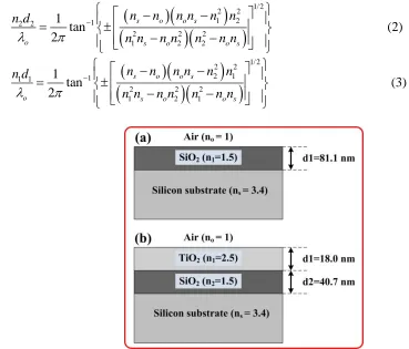
2.2 Design of SLAR and DLAR Coatings
The optimum thickness and refractive index with a minimum reflectance for a single-layer ARC can be deduced through the following equation:
1 1
4 o n d
(1)
where,
represents the mid-range wavelength of 500 nm, n1 and d1 represents the refractive index and layer thickness, respectively. A design diagram of SLAR coating is shown in Fig. 1(a).For the DLAR coating design, the high-low refractive index on the Si substrate (i.e., the upper film has the high refractive index and lower layer has low refractive index) was used. Schematic design of SiO2/TiO2 DLAR coating is shown in Fig. 1(b), where d1 and d2 represents the thickness of the outer and inner layers, respectively. Moreover, n0, n1, n2 and ns denote the refractive index of air, outer, inner films and substrate respectively. In order to achieve a zero reflectance each film must meet Eqs. (2) and (3) [24],
1/2 2 2 1 2 1 2 22 2 2
1 2 2
1 tan 2
s o o s
o s o o s
n n n n n n
n d
n n n n n n n
(2)
1/2 2 2 2 1 1 1 12 2 2
1 2 1
1 tan 2
s o o s
o s o o s
n n n n n n
n d
n n n n n n n
(3)
[image:4.596.78.447.418.733.2]
3. RESULTS AND DISCUSSION
[image:5.596.51.560.210.415.2]The film elemental analysis of SiO2 and SiO2/TiO2 ARC’s was investigated through energy dispersive x-ray spectroscopy (EDX) and surface morphology image was taken by FESEM (Fig. 2). The Fig. 2(a) shows the energy dispersive x-ray spectra of the different elements in SiO2 SLAR coating deposited on c-Si p-type (100). The elemental composition of the SiO2 layered silicon wafer was found to be dominated by Si (58.12 wt. %) followed by oxygen (41.68 wt. %).
Figure 2. EDX spectra (a) SiO2 film, (b) SiO2/TiO2 film.
It can be seen from spectra (fig. 2(b)) of SiO2/TiO2 layered silicon wafer, the dominance of silicon (48.98 wt. %) and titanium (27.15%) with oxygen (23.87%). Fig. 3(a) shows FESEM cross-section of Al-alloyed p+ layer formed at 850 ᵒC in ambient nitrogen condition.
[image:5.596.70.528.539.742.2][image:6.596.127.471.214.505.2]
FESEM Fig. 3(b) represents the AFM back view of Al-BSF layer on the Si substrate. Cross-section view shows the uniformity of Al-BSF layer along the Si substrate while little spikes of p+ layer can be seen in the back view of AFM micrograph.
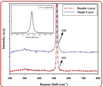
Fig. 4 shows the Raman spectra of the as-grown Si sample, SLAR SiO2 and DLAR SiO2/TiO2 coatings deposited on the c-Si p-type (100) using an Argon ion excitation laser source (514.5 nm) at room temperature. The as-grown Si sample produced a sharp solid line with a FWHM of 0.08 cm-1 located at 528.72 cm-1 because of the scattering of first-order phonons.
Figure 4. Raman spectra of the SiO2 and SiO2/TiO2 coatings deposited on the c-Si p-type (100).
Raman spectra of SiO2 SLAR layer deposited at room temperature shows one strong sharp peak at 520 cm-1 having FWHM of 9.3 cm-1. The absence of other features in the Raman spectra of SiO2 and SiO2/TiO2 films indicates the absence of other phases, such as amorphous Si phase. Raman spectra of SiO2/TiO2 DLAR layer shows one strong sharp peak at 519 cm-1 having FWHM of 9.9 cm-1. The Raman spectra of SiO2/TiO2 DLAR films do not contradict from that of the as-grown Si nor from the SiO2/Si one, that is in accordance with an amorphous state [25].
Figure 5. Shows the reflectance spectra for SLAR and DLAR coatings with the as-grown Si sample.
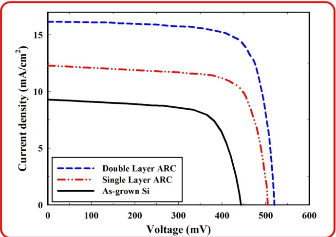
Figure 6. Shows the I-V graphs formed with SLAR (SiO2) and DLAR (SiO2/TiO2) coatings with the as-grown Si solar cell.
[image:7.596.126.471.386.629.2]
DLAR coatings, respectively. Reflection spectrum of SLAR SiO2 coating shows the minimum reflection of 11% at 530 nm while reflection spectrum of DLAR SiO2/TiO2 coating shows the minimum reflection of 2.3% at 630 nm within the 400-1000 nm range. Further, the DLAR reflectance is lower than 5% within the 540-760 nm wavelength range. It means the absorption of the incident photons was increased and hence the photo-generated current, which has significant effect in enhancing the solar cell efficiency.
The current–voltage characteristics of the solar cell devices with SLAR and DLAR coatings are shown in Fig. 6. The solar cells were characterized under 100 mW/cm2 illumination condition. It is given in Table 3 that the solar cell with DLAR SiO2/TiO2 coating has shown the best photovoltaic achievement, in special, a short circuit current Jsc of 16.1 mA/ cm2 which increases by ∆Jsc=6.9 mA/cm2 [8] related to the as-grown Si solar cell. On the other hand the results indicate the improved current density value as compared to Richards [18] for an optimized TiO2 DLAR coating. This consequently results in the improvement of cell efficiency to 6.2% which is an increase of 3.4% absolute in comparison to the as-grown Si solar cell.
[image:8.596.38.559.547.660.2]Further the solar cell with SLAR SiO2 coating has demonstrated the short circuit current Jsc of 12.3 mA/ cm2 which rises by ∆Jsc=3.1 mA/cm2 compared to the as grown Si cell. It enhances the cell efficiency by 4.5%, which is an improvement of 1.7% absolute in comparison to the as-grown Si cell. The addition of the TiO2 layer initiated 37% improvement in the efficiency of the DLAR SiO2/TiO2 coated Si solar cells, compared to 4.5% of the SLAR SiO2 coated Si solar cell. A similar photovoltaic efficiency result was obtained by Szlufcik and Majewski [16] for silicon solar cell. These indicate that the sputtering deposited SiO2 and TiO2 films can be used as DLAR ARCs for Si solar cells. The low temperature ARC depositions are also beneficial for the production of Si solar cells with minimum defects [28]. The Si solar cells with SLAR SiO2 and DLAR SiO2/TiO2 coatings show an increase of efficiency of about 60% and 214%, respectively, as compared to as-grown Si solar cell.
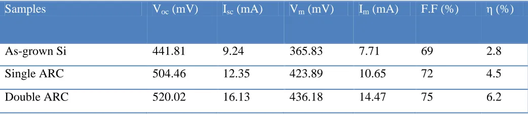
Table 3. Current–Voltage measurements of back surface field solar cells with and without ARC layers with the as-grown Si solar cell.
Samples Voc (mV) Isc (mA) Vm (mV) Im (mA) F.F (%) η (%)
As-grown Si 441.81 9.24 365.83 7.71 69 2.8
Single ARC 504.46 12.35 423.89 10.65 72 4.5
Double ARC 520.02 16.13 436.18 14.47 75 6.2
4. CONCLUSION
In this paper a preparation and comparison of high quality SLAR (SiO2) and DLAR (SiO2/TiO2) coatings on Si solar cells have been performed using sputtering technique at room temperature. Room temperature deposition of ARCs is feasible for making defects free solar cells. It is realized that the efficiency of solar cell with the DLAR (SiO2/TiO2) coating was better than that of SLAR (SiO2) solar cell. The reflectance of SLAR (SiO2) and DLAR (SiO2/TiO2) coatings were observed to be 15 and 7%, respectively. An enhancement of 214% and 60% in conversion efficiencies were obtained in the DLAR (SiO2/TiO2) and SLAR (SiO2) coated monocrystalline Si solar cells, respectively; as compared to the as-grown Si solar cell. The addition of the DLAR initiated 37% improvement in the efficiency of the monocrystalline Si solar cells, compared with 4.5% of the SLAR Si solar cell. Current-voltage characteristics have shown that the antireflection coatings have significant effect over the short circuit current of the solar cells. This addition of DLAR SiO2/TiO2 coating at low temperature sputtering conditions could be a significant contribution to currently well-known antireflective films for optoelectronic nano-devices as well as in silicon solar cells.
ACKNOWLEDGEMENT
The authors acknowledged the Short Term Research Grant Scheme (1001/PFIZIK/845015) and Universiti Sains Malaysia (USM) for the Fellowship to Khuram Ali.
References
1. M.-L. Kuo, D. J. Poxson, Y. S. Kim, F. W. Mont, J. K. Kim, E. F. Schubert and S.-Y. Lin, Opt. Lett., 33 (21) (2008) 2527.
2. M. Nam, J. Lee and K.-K. Lee, Microelectron. Eng., 88 (8) (2011) 2314.
3. S.-Y. Lien, D.-S. Wuu, W.-C. Yeh and J.-C. Liu, Sol. Energ. Mat. Sol. C., 90 (16) (2006) 2710. 4. K. Ali, S. A. Khan and M. MatJafri, Int. J. Electrochem. Sci., 8 (6) (2013) 7831.
5. K. Ali, S. Khan and M. Jafri, Nanoscale. Res. Lett., 9 (1) 1-6 (2014). 6. K. Ali, S. A. Khan and M. Z. Mat Jafri, Sol. Energy, 101 (0) (2014) 1.
7. Ö. Kesmez, H. Erdem Çamurlu, E. Burunkaya and E. Arpaç, Ceram. Int. 36 (1) (2010) 391.
8. D. Hocine, M. S. Belkaid, M. Pasquinelli, L. Escoubas, J. J. Simon, G. A. Rivière and A. Moussi, Mater. Sci. Semicond. Process., 16 (1) (2013) 113.
9. B. G. Lee, J. Skarp, V. Malinen, L. Shuo, C. Sukgeun and H. M. Branz, presented at the Photovoltaic Specialists Conference (PVSC) 2012 38th IEEE, 2012.
10.N. Ahmed, C. B. Singh, S. Bhattacharya, S. Dhara and P. B. Bhargav, Conference Papers in Energy 2013 4 (2013).
11.C.-H. Yang, S.-Y. Lien, C.-H. Chu, C.-Y. Kung, T.-F. Cheng and P.-T. Chen, Int. J. Photoenergy 2013 (2013) 1.
12.J. Li, Y. Lu, P. Lan, X. Zhang, W. Xu, R. Tan, W. Song and K.-L. Choy, Sol. Energy 89 (0) (2013) 134.
13.B. S. Richards, S. F. Rowlands, A. Ueranatasun, J. E. Cotter and C. B. Honsberg, Sol. Energy 76 (1–3) (2004) 269.
15.G. F. Perez-Sanchez, M. de la Luz Perez and A. Morales-Acevedo, presented at the Electrical and Electronics Engineering, 2005 2nd International Conference on, 2005.
16.J. Szlufcik, J. Majewski, A. Buczkowski, J. Radojewski, L. Jȩdral and E. B. Radojewska, Sol. Energ. Mat., 18 (5), (1989) 241.
17.S. Schiller, G. Beister, W. Sieber, G. Schirmer and E. Hacker, Thin Solid Films 83 (2) (1981)239. 18.B. S. Richards, Sol. Energ. Mat. Sol. C., 79 (3) (2003) 369.
19.L. M. Doeswijk, H. H. C. de Moor, D. H. A. Blank and H. Rogalla, Appl Phys A 69 (1) S409-S411 (1999).
20.S. F. Pellicori, Sol. Cells 3 (1) (1981) 57.
21.S. J. Oh, S. Chhajed, D. J. Poxson, J. Cho, E. F. Schubert, S. J. Tark, D. Kim and J. K. Kim, Opt Express 21 (101) (2013) A157.
22.M. J. Ariza, F. Martín and D. Leinen, Surf. Interface Anal., 35 (3) (2003) 251. 23.M. J. Ariza, F. Martín and D. Leinen, Appl. Phys. A 73 (5) (2001) 579.
24.H. A. Macleod, Thin-Film Optical Filters, second ed. (Macmillan Publishing Company, New York, 1986).
25.A. Hodroj, O. Chaix-Pluchery, M. Audier, U. Gottlieb and J.-L. Deschanvres, J. Mater. Res., 23 (03) (2008) 755.
26.Richards BS: Novel uses of titanium dioxide for silicon solar cells. Center for Photovoltaic Engineering; 2002.
27.P. Panek, K. Drabczyk, A. Focsa, A. Slaoui. Mat. Sci. Eng. B, 165 (2009) 64. 28.M. Ariza, F. Martin, D. Leinen. Surf. Interface. Anal., 35 (2003) 251.
29.S. J. Lee, M. G. Hur and D. H. Yoon, J. Nanosci. Nanotechnol., 13 (11) (2013) 7664.
30.V. Baglio, M. Girolamo, V. Antonucci and A. Aricò, Int. J. Electrochem. Sci., 6 (8) (2011) 3375.