N A N O E X P R E S S
Open Access
Phosphorus diffusion gettering process of
multicrystalline silicon using a sacrificial porous
silicon layer
Derbali Lotfi
*and Ezzaouia Hatem
Abstract
The aims of this work are to getter undesirable impurities from low-cost multicrystalline silicon (mc-Si) wafers and then enhance their electronic properties. We used an efficient process which consists of applying phosphorus diffusion into a sacrificial porous silicon (PS) layer in which the gettered impurities have been trapped after the heat treatment. As we have expected, after removing the phosphorus-rich PS layer, the electrical properties of the mc-Si wafers were significantly improved. The PS layers, realized on both sides of the mc-Si substrates, were formed by the stain-etching technique. The phosphorus treatment was achieved using a liquid POCl3-based source on both sides of the mc-Si wafers. The realized phosphorus/PS/Si/PS/phosphorus structures were annealed at a temperature ranging between 700°C and 950°C under a controlled O2atmosphere, which allows phosphorus to diffuse
throughout the PS layers and to getter eventual metal impurities towards the phosphorus-doped PS layer. The effect of this gettering procedure was investigated by means of internal quantum efficiency and the dark current–voltage (I-V) characteristics. The minority carrier lifetime measurements were made using a WTC-120 photoconductance lifetime tester. The serial resistance and the shunt resistance carried out from the darkI-Vcurves confirm this gettering-related solar cell improvement. It has been shown that the photovoltaic parameters of the gettered silicon solar cells were improved with regard to the ungettered one, which proves the beneficial effect of this gettering process on the conversion efficiency of the multicrystalline silicon solar cells.
Keywords:Multicrystalline silicon, Porous silicon, Defect density, Grain boundaries, Gettering, WTC-120 lifetime tester
Background
Due to the high price of fossil energy source and huge pollution of environmental issue, in the recent years, the development of renewable energy has regained our at-tention. The development of the solar energy industry is one of the most popular technologies in renewable energy. The majority of solar cells are made from crys-talline silicon; more than half of the cryscrys-talline silicon solar cell production is based on multicrystalline silicon (mc-Si). The quality of multicrystalline silicon (mc-Si) wafers may become worse in the future for several rea-sons; the main reason is that lower-quality feedstock will probably be used for cost reduction and availability rea-sons [1]. Improving conversion efficiency using a
low-cost material development is the main research activity in the photovoltaic field [2,3]. Several experiments de-monstrated that the electrical properties of crystalline sili-con solar cells can be improved by coating the n + emitter region with a porous silicon layer [2-5], and many tech-nologies have been used for this purpose [6-8], such as using vanadium oxide as an antireflection coating [9]. The possibility of improving the electrical properties of silicon wafers, by extracting impurities from them, using thermal treatment under oxygen atmosphere, or phosphorus dif-fusion, is well known [10-13]. Besides, the porous silicon (PS) layer may be used as an efficient sacrificial layer for gettering metallic impurities [11,14]. There are two gene-ral classifications of gettering, namely extrinsic and intrin-sic. Extrinsic gettering refers to gettering that employs external means to create the damage or stress in the sili-con lattice in such a way that extended defects needed for
* Correspondence:[email protected]
Photovoltaïc laboratory, Research and Technology Center of Energy, Technopôle de Borj-Cédria. BP 95, Hammam-Lif 2050, Tunisia
trapping impurities are formed. These chemically reactive trapping sites are usually located at the wafer surfaces, away from the bulk. Intrinsic gettering is using oxygen to enforce precipitation of metallic impurities, such as cop-per, not at the wafer surface but in its bulk. A preparatory step in this case is a thermal treatment causing precipita-tion of the excess oxygen which, for a variety of reasons related to the specific properties of oxygen in silicon, forms oxygen precipitates in the bulk of the wafer rather than at its surface. Those oxygen precipitates then act as gettering sites for metallic impurities. PS may also be used as an excellent antireflective coating or as a passivating layer on the emitter of crystalline silicon [15]. Most often, the formation of PS can create defects in the surface of the Si substrate that may enhance the gettering effect as extrinsic gettering effect. A phosphorus gettering model was proposed [16], which stated that the gettering speed is controlled by two steps. The first step is to limit the get-tering temperature by releasing diffusion of metal impu-rities, and the second step is to control the best gettering temperature by the segregation function. Other authors [17] proposed that silicon self-interstitial current gener-ated during phosphorus (P) diffusion is an essential factor of the gettering mechanism, and also found that Fermi level-enhanced solubility in the P diffused layer contri-butes to the gettering effect. The use of an infrared (IR) furnace for the fabrication of p-n junction [18,19] and get-tering impurity through the porous silicon layer [20] is one of the processes that may be used to reach this goal. In this work, we will investigate the increase of carrier lifetime and the conversion efficiency of multicrystalline silicon solar cells gettered by a phosphorous gettering pro-cess using a sacrificial porous silicon layer in which the impurities will be trapped.
Methods
The starting material was a p-type (boron-doped) multi-crystalline silicon substrate, 400 μm thick with a resisti-vity of 1 to 2 Ω cm. To avoid changes in grains and grain barriers (GBs) from wafer to wafer, samples were selected from consecutive mc-Si wafers sharpened suc-cessively in the same ingot. Similar wafers, which were vertically adjacent to each other in the ingot, were used to compare and confirm the gettering effect. Therefore, differences between them, after different processing, can be interpreted as being due to variations in the process parameters rather than to material variations. PS layers were formed on both sides by the stain-etching tech-nique using HF/HNO3/H2O solution with a 1:3:5 volume composition [3]. A POCl3/acetone liquid source was used for the diffusion process [20]. We optimized the POCl3/ acetone ratio to 1:5. The POCl3spreading out was realized by the spinning technique onto p-type multicrystalline sili-con wafers. After drying at 200°C for solvent evaporation,
the realized P/PS/Si/PS/P structure undergoes a heat treatment in an IR furnace under an O2atmosphere. The temperature annealing was varied in the range of 700°C to 950°C for 60 min. This heat treatment has been applied in order to allow P diffusion throughout the PS layer. After annealing the samples, the phosphorous-doped re-gion (the phosphorous-doped PS layer) was removed from both sides using a chemical etching (HF 16%: HNO364%: CH3COOH 20%) solution. In order to perform the solar cell fabrication process, the n+/p junction was achieved using a simple phosphorus diffusion technique. The back aluminum (Ag/Al) and the front Ag contacts were screen printed using AMI Presco CP885 screen printer (Affiliated Manufacturers, Inc., North Branch, NJ, USA) and fired at 850°C and 620°C, respectively. The gettering effect has been evaluated by measuring the minority carrier lifetime, the dark and illuminatedI-Vcharacteristics, and the defect density at the GBs of the mc-Si substrates. TheI-V mea-surements under illumination have been performed using PASAN cell tester CT 801 (PASAN Measurement Systems, Neuchâtel, Switzerland). The effective minority carrier lifetime (τeff) in the mc-Si substrates was measured using a WTC-120 photoconductance lifetime tester (Sinton Instruments, Boulder, CO, USA) under the quasi-steady-state lifetime measurement using the generalized analysis condition.
Results and discussion
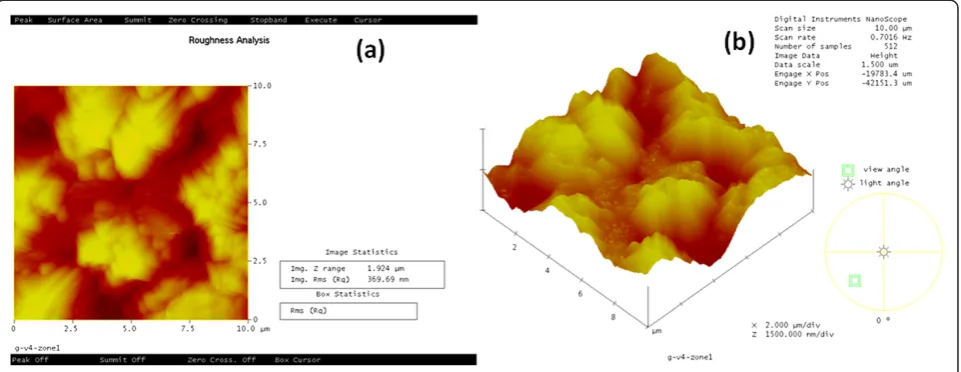
The porous silicon layer created onto the front and back surfaces of the multicrystalline silicon wafers has a great importance in this work because it has the role of an ex-ternal trapping site of impurities extracted from the sam-ples. Figure 1a,b presents an atomic force microscopy (AFM) topography of the porous silicon layer formed by the stain-etching technique.
The porous silicon structure has been treated with phosphorus, followed by heat treatment at various tem-peratures ranging between 700°C and 950°C. Then, the treated PS layers were removed, and as a result, purified mc-Si substrates have been obtained. To confirm this get-tering effect on the electrical properties of the samples, we have investigated the variation of the effective minority carrier lifetime.
significant effect. The lifetimes reported here should be considered as effective lifetimes, which include both sur-face and volume recombination components. In many practical cases, there may be several sources of recombin-ation in a sample, such as recombinrecombin-ation through impur-ities in the wafer bulk or recombination at the surfaces. The effective lifetime represents the combined impact of all of these competing recombination channels. The ef-fective lifetime τeff measured under low-level injection at
Δn= 1 × 1014 cm-3 was taken for the calculations under generalized conditions. For 2 Ωcm (the resistivity of the wafers) and ND= 5 × 1014cm-3, the wafers satisfy the low-level injection condition (Δn< <ND).
The effectiveness of this gettering process is confirmed by the increase of the minority carrier lifetime, measured at the same carrier density, before and after treatment. Table 1 summarizes the effect of this treatment process on the effective minority carrier lifetime (τeff). We have obtained a very high lifetime value of the minority car-rier after a thermal treatment at 900°C. We notice that τeffincreases when the annealing temperature increases, as shown in Table 1.
Multicrystalline silicon incorporates many impurities and defects that limit the minority carrier lifetime and, thus, the solar cell performance [21]. This significant va-riation of the minority carrier lifetime would indicate that a non-negligible quantity of unwanted impurities has been gettered and removed from the Si material and a decrease of the grain and GBs carrier recombination activities. Considering that the measurement area in-cludes several grain boundaries, the results presented here indicate a very low recombination activity at the grain boundaries when comparing treated wafers to untreated one (reference).
It is important to note that the surface and volume re-combination mechanisms coexist. We considered that both front and back surfaces of the wafer are identical since both of them have been subjected to the same treatment. The equation that takes into account all the recombination mechanisms that are present in the wafer is given by [22]:
1 τeff¼
1 τbulkþ
2S
W:
Supposing that both front and back surfaces of all samples were subjected to the same passivation effect and have the same surface state, we can neglect the ef-fect of the surfaces [22,23]. Consequently, (τbulk) can be deduced:
1 τeff∝
1 τbulk:
[image:3.595.59.540.90.276.2]Therefore, we can determine the bulk recombination properties of the wafer from the effective minority car-rier lifetime measurements. As a result, the obtained
Table 1 Measured effective lifetimeτeffunder low-level injection
Temperature (°C) τeff(μsec)
Reference 2.92
700 37.17
800 59.76
850 83.16
900 90.88
950 13.07
τeff, effective minority carrier lifetime.
[image:3.595.306.540.627.725.2]improvement indicates that impurities in the bulk of the treated wafers have been removed, and the recombina-tion activities have been decreased noticeably.
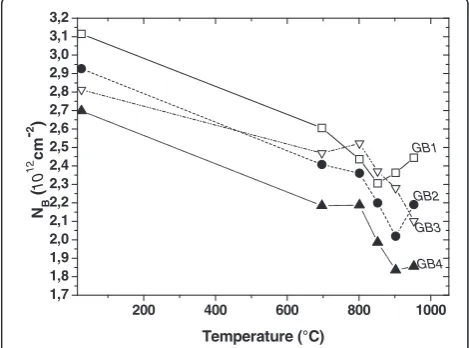
It is now interesting to investigate the variation of the defect density at the GBs while changing the treatment conditions, which is a one of the important parameters to evaluate the effect of our gettering process. We have performed four aluminum ohmic contacts on two adja-cent grains (as shown in Figure 2). The aluminum was deposited by screen printing using Al/Ag containing aluminum and a small amount of silver in order to en-sure the welding of the contact’s edges. A DC current passes through the selected GBs between two adjacent grains using two external contacts. Using the two inner contacts, we have measured the voltage U. Figure 2 shows a schematic illustration of the dark I-V measure-ments across four selected GBs to evaluate the defect density (NB) [24].
The zero-bias conductance for grain boundary is de-fined by [24,25]:
σB¼JDC U
whereUis the applied voltage. It can be written as [26]:
σB¼
1
RS¼ e2
KTNaνtð1CÞexpðKTVBÞ
The GB potential barrier can be written as following:
VB¼KTLog eANaS
NvσBKT
where K is the Boltzmann constant, T is the ambient temperature, e is the elementary charge, A is the Richardson constant, andSis the grain boundary surface crossed by the current flow. Nvand Naare the effective densities of the valence states and the doping concentra-tion, respectively.
The defect density NB(cm-2) was determined as a func-tion of the GB potential barrierVB[27]:
NB¼QBe ¼
ffiffiffiffiffiffiffiffiffiffiffiffiffiffiffiffiffiffiffiffiffiffiffiffi 32εγε0NaVB p
e :
Identical wafers have been treated and identical GBs in the gettered samples show that defect density decreases when samples were subjected to thermal treatment, as shown in Figure 3. This significant variation of the defect density at the GBs would indicate that a non-negligible quantity of undesirable impurities have been gettered and removed from the grain boundaries. Thus, the recombi-nation activities at the GBs have been reduced noticeably. These improvements could be attributed to the removal of eventual bulk metal impurities (Fe, Cu, etc.) and their trapping into the n+/PS layer. We notice that high-temperature annealing in infrared furnace has enhanced the impurity diffusion into the sacrificial porous silicon layer. Thus, the phosphorus-rich PS acts as an efficient ex-ternal gettering site in which the impurities are captured due to the high thermal treatment. The phosphorus diffu-sion into grain boundaries, at least in the region near the front and back surfaces, can explain the considerable
200 400 600 800 1000 1,7
1,8 1,9 2,0 2,1 2,2 2,3 2,4 2,5 2,6 2,7 2,8 2,9 3,0 3,1 3,2
NB
(
10
12
cm
-2 )
Temperature (°C)
GB1
GB3
[image:4.595.54.541.88.230.2]GB4 GB2
Figure 3Effect of annealing the PS/phosphorus structure on the defect density at four selected GBs.
Applied voltage DC current injection
GB
mc-Si substrat
[image:4.595.304.539.523.697.2]IDC U
decrease of the defect density and the recombination ac-tivities into the GBs, as shown in Figure 3.
To understand the impact of this gettering process on cell performance, the internal quantum efficiency (IQE) measurements were evaluated at various annealing tem-peratures. All annealing temperatures exhibit an increa-sed blue response in short wavelengths (400 to 750 nm), which is due to an important decrease of the surface re-combination velocity and an improvement of the carrier collection at the emitter region, as shown in Figure 4.
A significant increase of the IQE in the long-wave-length range 700 to 1,000 nm (red response) is observed. This improvement can be explained by the important reduction of the carrier recombination activities in the bulk of the treated wafers, which is proven by the ob-tained minority carrier lifetime values in Table 1, and the significant reduction of the defect density at the GBs, at least in the region near the front and back sur-faces. The observed behavior of the spectral response indicates that our gettering process leads to an efficient surface and bulk passivation and indicates an extended effect deep into the bulk of the substrate, which we sug-gest to be considered especially at the grain boundaries. The gettered solar cell at 900°C shows the highest IQE, which is not surprising because the effective lifetime of the minority carrier in the wafer treated at 900°C proved to be the highest.
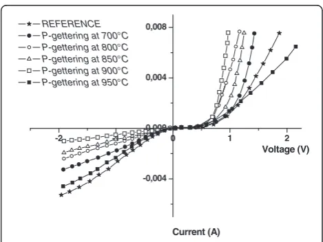
[image:5.595.56.291.88.274.2]The dark I-Vcharacteristics have been investigated in Figure 5. After PS treatment, a significant improvement in the typical dark I-Vcharacteristic was observed: the leakage current has considerably decreased, which is due to the reduction of the impurity concentration by get-tering undesirable metallic impurities and defects that
diffuse at getter sites present at the pore walls of the phosphorous-rich PS layer. TheI-Vcharacteristics clearly show a significant improvement of the rectifying behavior and a noticeable decrease of the reverse current after treatment, indicating an efficient passivation of grain and grain boundaries of the mc-Si wafers.
In multicrystalline silicon solar cells, the saturation current is essentially due to short circuiting via GBs. The current–voltage characteristic of the gettered samples shows an enhancement of the saturation current, which is a sign of the passivation effect of this gettering process at GBs. From these darkI-Vcurves, we determined the series resistance (Rs) [28] and the shunt resistance (Rsh) of the gettered and untreated cells.
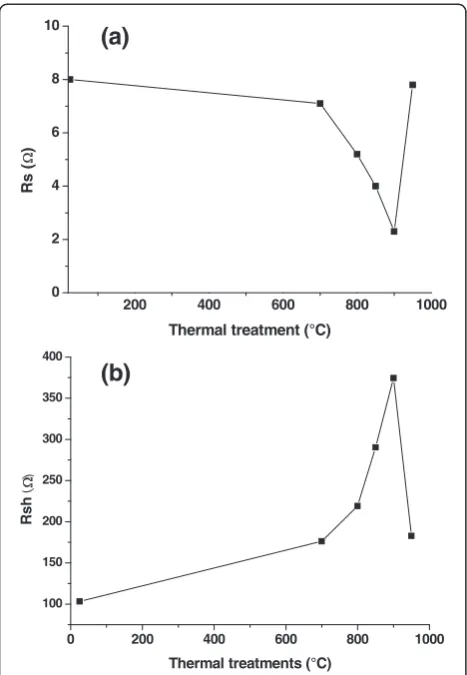
Figure 6 depicts the variation of the series and shunt resistances. We notice a significant increase of the shunt resistance (Rsh) and a diminution of the series resistance (Rs). The improvement ofRsh can be attributed to an ef-ficient passivation of the grain and GBs of the mc-Si wafers and the gettering of unwanted impurities.
However, the enhancement of Rs could be due to the gettering effect in adjacent grains [29]. The deep recom-bination centers present at the GBs and bulk defects have been reduced, and an important decrease of the surface recombination velocity has been obtained. Get-tering at 950°C seems to have a bad effect on the elec-trical properties of the cells, which could be due to the deep diffusion of phosphorus into the mc-Si substrate when annealing the sample at 950°C.
In Figure 7, we carried out the I-Vcharacteristic mea-surement of obtained solar cells under AM1.5 illumina-tion (100 mW/cm2). Four parameters of solar cells were used to define illuminated solar cells: the short-circuit current (Isc), the open-circuit voltage (Voc), the fill factor (FF), and the efficiency (η).
-2 -1 0 1 2
-0,004 0,000 0,004 0,008
Current (A)
REFERENCE P-gettering at 700°C P-gettering at 800°C P-gettering at 850°C P-gettering at 900°C P-gettering at 950°C
[image:5.595.304.539.523.699.2]Voltage (V)
Figure 5DarkI-Vcharacteristics of the untreated and the PS-gettered samples at 700°C, 800°C, and 900°C.
400 500 600 700 800 900 1000 1100 0
10 20 30 40 50 60 70 80 90 100
Reference (untreated) Sample treated at 950°C Sample treated at 800°C Sample treated at 850°C Sample treated at 900°C Sample treated at 700°C
IQ
E (%)
Wavelength (nm)
The optimal temperature is about 900°C. This op-timum could be the result of the competition between the release of impurities from the bulk and a capture of
[image:6.595.57.291.88.426.2]impurities in the gettering layer, which has been re-moved after the thermal treatment. Below the optimum temperature, gettering process is limited by the release or the diffusion [28,30] of metallic impurities towards the gettering layer. This behavior is confirmed by the degradation of the I-V characteristics for the samples treated at temperatures exceeding the optimum one.
Table 2 shows the variation of theIscand theVocafter phosphorous gettering at different temperatures. Our gettering process improves the Isc from 74 to 109 mA (sample gettered at 900°C) and the Voc from 0.48 to 0.55 mV (sample gettered at 900°C). The effect of gette-ring mc-Si using the combination of phosphorous diffu-sion into a sacrificial PS layer and a thermal treatment becomes apparent when looking at the different cell para-meters. The untreated solar cell (reference sample) shows a drastically lower short-circuit current density (Jsc) com-pared to the cells subjected to the above treatment, espe-cially when annealed at 900°C. The same tendency can be stated for the open-circuit voltage (Voc), which is 70 mV higher in the case of the gettered solar cell at 900°C, com-pared to the reference wafer (untreated). We conclude that phosphorous gettering process under O2atmosphere, using a sacrificial PS layer on both sides, improves the electrical parameters and the performances of the cells via the reduction of the carrier recombination activities. This leads to an enhancement of the short-circuit current and the open-circuit voltage and an increase of the conversion efficiency of the mc-Si solar cells.
Conclusions
The application of a sacrificial porous silicon layer, fol-lowed by a deposition of thin POCl3liquid film and then subjecting to a thermal treatment, has been proven to be able to getter undesirable impurities from the mc-Si sub-strate. The best results were achieved after gettering at 900°C for 60 min. This gettering process has led to a sig-nificant increase of the minority carrier lifetime and a no-ticeable decrease of the defect density at grain boundaries. The improvement of the internal quantum efficiency con-firms the beneficial effect of the above treatment.
0 100 200 300 400 500 600 700
0 30 60 90 120 150
reference 700°C 800°C 900°C 850°C
I (
m
A)
[image:6.595.56.292.517.695.2]V (mv)
[image:6.595.304.540.633.716.2]Figure 7I-Vcharacteristics under AM1.5 illumination of the gettered multicrystalline solar cells.
Table 2 Comparison of the electrical parameters of phosphorous gettered and ungettered multicrystalline silicon solar cells
Temperature (°C) Jsc(mA/cm²) Voc(V) FF η
Reference 18.5 0.48 67 5.9
700 21.3 0.50 69.4 7.4
800 24.4 0.52 70.5 8.9
850 26.3 0.53 74.8 10.4
900 27.4 0.55 77.2 11.6
FF, fill factor;Jsc, short-circuit current density;Voc, open-circuit voltage; η, efficiency.
200 400 600 800 1000 0
2 4 6 8 10
Rs (
)
Thermal treatment (°C)
(a)
0 200 400 600 800 1000 100
150 200 250 300 350 400
Rsh
(
)
Thermal treatments (°C)
(b)
Impurities and defects at the surfaces and at the GBs have been trapped inside the P-doped PS layer after the heat treatment. Obtained results show a significant improve-ment of the electrical performances of the mc-Si solar cells, and the conversion efficiency has been increased from 5.9% to 11.6% in the sample gettered at 900°C.
Competing interests
The authors declare that they have no competing interests.
Authors' contributions
DL carried out the synthesis and analysis of the experiment, fabricated the porous silicon layers, measured the minority carrier lifetime and performed the AFM imaging and IQE andI-Vmeasurements of the gettered solar cells. DL and HE contributed to the conception and design of the experiments, data interpretation and writing of the manuscript, discussed the results, contributed to the manuscript text, commented on the manuscript and approved its final version. Both authors read and approved the final manuscript.
Received: 29 April 2012 Accepted: 5 July 2012 Published: 31 July 2012
References
1. Bakos GC:Distributed power generation: a case study of small scale PV power plant in Greece.Appl Energy2009,86:1757–1766.
2. Yamaguchi M, Ohshita Y, Arafune K, Sai H, Tachibana M:Present status and future of crystalline silicon solar cells in Japan.Solar Energy2006, 80:104–110.
3. Krotkus A, Grigoras K, Pacebutas V, Barsony I, Vazsonyi E, Fried M, Szlufcik J, Nijs J, Lévy-Clément C:Efficiency improvement by porous silicon coating of multicristalline silicon solar cells.Sol Energy Mater Sol Cells1997, 45:267–273.
4. Yae S, Kobayashi T, Kawagishi T, Fukumuro N, Matsuda H:Antireflective porous layer formation on multicrystalline silicon by metal particle enhanced HF etching.Solar Energy2006,80:701–706.
5. Bastide S, Albu-Yaron A, Strehlke S, Lévy-Clément C:Formation and characterization of porous silicon layers for application in multicrystalline silicon solar cells.Sol Energy Mater Sol Cells1999,57:393.
6. Ben Rabha M, Hajjaji A, Bessais B:Improvement of multicrystalline silicon solar cell performance via chemical vapor etching method-based porous silicon nanostructures.Solar Energy2012,86:1411–1415.
7. Macdonald DH, Cuevas A, Kerr MJ, Samundsett C, Ruby D, Winderbaum S, Leo A:Texturing industrial multicrystalline silicon solar cells.Solar Energy 2004,76:277–283.
8. Richards BS, Rowlands SF, Ueranatasun A, Cotter JE, Honsberg CB:Potential cost reduction of buried-contact solar cells, through the use of titanium dioxide thin films.Solar Energy2004,76:269–276.
9. Ben Rabha M, Bessais B:Enhancement of photovoltaic properties of multicrystalline silicon solar cells by combination of buried metallic contacts and thin porous silicon.Solar Energy2010,84:486–491. 10. Derbali L, Ezzaouia H:Vanadium-based antireflection coated on
multicrystalline silicon acting as a passivating layer.Solar Energy2012, 86:1504–1510.
11. Goetzberger A, Shockley W:Metal precipitates in Silicon p-n junctions.
J Appl Phy1821,1960:31.
12. Derbali L, Dimassi W, Ezzaouia H:Improvement of the minority carrier mobility in low-quality multicrystalline silicon using a porous silicon-based gettering under an O2atmosphere.Energy Procedia2011, 10:243–248.
13. Ponce-Alcantara S, Del Canizo C, Luque A:Adaptation of monocrystalline solar cell process to multicrystalline materials.Sol Energy Mater Sol Cells 2005,87:411.
14. Khedher N, Hajji M, Hassen M, Ben Jaballah A, Ouertani B, Ezzaouia H, Bessais B, Selmi A, Bennaceur R:Gettering impurities from crystalline silicon by phosphorus diffusion using a porous silicon layer.Sol Energy
Mater Sol Cells2005,87:605.
15. Bilyalov R, Stalmans L, Beaucarne G, Loo R, Caymax M, Poortmans J, Nijs J: Porous silicon as an intermediate layer for thin-film solar cell.Sol Energy
Mater Sol Cells2001,65:477.
16. Bilyalov RR, Ludermann R, Wettling W, Stalmans L, Poortmans J, Nijs J, Schirone L, Sotgiu G, Strehlke S, Lévy-Clément C:Multicrystalline silicon solar cells with porous silicon emitter.Sol Energy Mater Sol Cells2000, 60:391.
17. Kang JS, Schroeder DK:Gettering in silicon.J Appl Phys1989,65:2974. 18. Schrôter W, Kuhnaplef:Model describing phosphorus diffusing gettering
of transition elements in silicon.Appl Phy Lett1990,56:2207. 19. Szlufcik J, Duerinckx F, Horzel J, Van Kerschaver E, Einhaus R, De Clerca K,
Dekkers H, Nijs J:Advanced concepts of industrial technologies of crystalline silicon solar cells.Opto-Electron Rev2000,8:299. 20. Noêl S, Lautenschlqger H, Muller JC:Highest efficiency rapid thermal
processed multicrystalline silicon solar cells.Prog Photovolt2001,9:41. 21. Khedher N, Hajji M, Bouaîcha M, Boujmil MF, Ezzaouia H, Bessais B,
Bennaceur R:Improvement of transport parameters in solar grade monocrystalline silicon by application of a sacrificial porous silicon layer.
Solid State Commun2002,123:7.
22. Sopori B:Silicon solar-cell processing for minimizing the influence of impurities and defects.J Electron Mater2002,31:972–980.
23. Cuevas A, Macdonald D:Measuring and interpreting the lifetime of silicon wafers.Solar Energy2004,76:255–262.
24. Kampwerth H, Rein S, Glunz SW:Proceedings of the Third World Conference on Photovoltaic Energy Conversion: May 18 2003. InPure experimental determination of surface recombination properties with high
reliability. Osaka. New York: IEEE Proceedings; 2003:1073–1076.
25. Nouri H, Bouaicha M, Bessais B:Effect of porous silicon on the performances of silicon solar cells during the porous silicon-based gettering procedure.Solar Energy Materials & Solar Cells2009, 93:1823–1826.
26. Môller HJ:Semiconductors for Solar Cells. Boston, MA: Artech House, Inc; 1993:187.
27. Pollok AG, Deline VR, Furman BK:Grain Boundaries in Semi-conductors. Amsterdam: Elsevier Science; 1982:71.
28. Greuter F, Blatter G:Electrical properties of grain boundaries in polycrystalline compound semiconductors.Semicond Sci Technol1990, 5:111–137.
29. Priyanka, Lal M, Singh SN:A new method of determination of series and shunt resistances of silicon solar cells.Sol Energy Mater Sol Cells2007, 91:137.
30. Green MA:Crystalline and thin-film silicon solar cells: state of the art and future potential.Solar Energy2003,74:181.
doi:10.1186/1556-276X-7-424
Cite this article as:Lotfi and Hatem:Phosphorus diffusion gettering process of multicrystalline silicon using a sacrificial porous silicon layer. Nanoscale Research Letters20127:338.
Submit your manuscript to a
journal and benefi t from:
7Convenient online submission
7Rigorous peer review
7Immediate publication on acceptance
7Open access: articles freely available online
7High visibility within the fi eld
7Retaining the copyright to your article