International Journal of Innovative Technology and Exploring Engineering (IJITEE) ISSN: 2278-3075, Volume-8 Issue-8, June 2019
Abstract: This paper presents a low complicated algorithm for balancing voltage intending to diminish the power switches switching frequency and control technique to limit the harmonic currents that circulate in Modular Multilevel converter. This algorithm is generally very simple without any extra execution prerequisites and is effectively expandable to any number of submodules (SMs). This balancing control strategy reduces all the capacitors voltage ripple magnitude. The modulation technique utilized is phase-disposition pulse width modulation (PD-PWM) which gives better outcomes contrasted with other balance strategies. It is demonstrated that the proposed control technique gave better execution of decrease of circulating harmonic currents. The total harmonic distortion (THD) of the output Phase and Line voltages are benchmarked against this control strategy. The outcomes are confirmed through MATLAB /Simulink software.
Index Terms: PD-Pulse Width Modulation, Voltage balancing algorithm, Circulating current control
I. INTRODUCTION
With the advancement of higher ratings of equipment related to power electronics that can be used for different medium to high-voltage applications keep on profiting by the headway of the fully controlled high-power semiconductors [1]. Applications include the engine drives, traction systems [1], high voltage direct current (HVDC) power transmission, flexible alternating current transmission systems (FACTS, such as static compensators (STATCOMs) to specify only a few [2]). It is necessary that the range of voltage and power need to be raised for certain applications, such as the quick improvement of multilevel voltage source converters (VSCs) in the course of the most recent decades has come about, for example, economically effective practical HVDC systems [3]. The staircase approximation of the sinusoidal waveform in multilevel converters with various DC sources is utilized, which help in the adequate decrease in the total harmonic distortion (THD) of the voltage obtained. Distinct topologies were introduced for such energy conversion of solid-state systems, which include the converter that is clamped at the diode, neutral point-clamped (NPC), the capacitor-clamped (flying capacitor, FC) converter and the cascaded converter
Revised Manuscript Received on
Mudadla Venkatesh, EEE Department, GMRIT, Rajam, India.
Dr.K.Chandra Sekhar, EEE Department, RVR & JC College of Engineering, Guntur,India.
(CC)[4].
The neutral point-clamped (NPC) consists of a unique DC-bus along with capacitors in progression being subdivided into different levels of voltage. Thus, the required levels of voltage can be obtained without any utilization of transformer. In this case, increase in count of levels increase the converter’s controller complexity and also the voltage balance of the capacitors. The flying capacitor-clamped (FC) converters include capacitors inside a phase leg that get charged to various voltage levels. It imparts numerous advantages to the NPC whereas the capacitors rating with respect to voltage has serious disadvantages that hinder the development of the converter with sensibly greater levels. The cascaded converter (CC) includes full-bridge topological arrangement in series in order to get a waveform indicating multilevel voltage. Each full-bridge has an isolated control and protection, also alternate DC power supply is provided to each level which expands the size and increase the converter cost. Topologies, like the cascaded converter, using capacitors rather than DC-sources likewise were illustrated [5]. The MMC is a fascinating multilevel converter with enormous advantages, for example, particularly in development point of view; an MMC can provide a multilevel waveform with a substantial number of steps along with managing faults. An MMC can be arranged by utilizing half-or full-bridge circuits and their relevant capacitors. The utilization of various full-bridge sub-modules results in an AC/AC converter by connecting the sub-modules to form phase-legs. Likewise, the utilization of a half-bridge sub-modules, or DC-choppers, being cascaded with phase-legs results a DC/AC converter.
The latter proposed converter topology can work similarly as a consecutive design for HVDC control transmission system or to control a motor, without any need of an extensive DC-side capacitor. These decrease the expenses of the converter and expand its unwavering quality. In addition to it, it is vital to report the impacts of the control technique to various factors, for example, the combination of the waveforms of voltage, the charging and discharging of the floating capacitors, the losses during switching, and total harmonic distortion.
A Heuristic Controller for AC Circulating
Current components elimination in Modular
Multilevel Converter
II. THE PRINCIPLE OPERATION OF MMC
Generally, a three-phase MMC has a dual arm along each phase unit and each arm consists of N sub-modules associated in an arrangement shown in Fig.(1). The
Fig(1) : Three Phase MMC circuit diagram
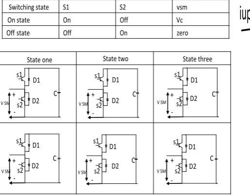
half-bridge submodule comprises of two switches (S1 & S2), a capacitor and its proportionate circuit appears in (Fig. 2). The switches comprise of an IGBT along with a freewheeling diode which is connected in antiparallel with it. In typical activity, only one of the switches operate at a given instant of time. Based upon the current direction the capacitor either charge or discharge.
At a given point of time, when a single IBGT is switched on, either the corresponding IGBT or the concerned freewheeling diode present in the equivalent submodule would conduct, contingent to the current direction at that instant, and thus it bodes well to characterize that a sub-module is on, which indicate that either the IGBT or the diode is conducting.
Three conceivable exchanging states could be characterized as shown in Fig (2).
• Firstly, in inserted or ON state, S1 remain on and S2 remain off. The sub-module voltage (VSM), levels with the voltage of
capacitor (VC) and the capacitor gets charged if the current at
that instant is positive else get discharged.
• Secondly, in bypassed or OFF state S2 remain on and S1 remain off. The voltage of sub-module (VSM) becomes zero
and the capacitor voltage remains consistent, for example, the capacitor neither charge nor discharge.
• Thirdly, in blocked state, the two switches remain off, and hence the freewheeling diodes start conducting. The capacitor gets charged if the direction of the current is positive, however it can't discharge.
Each phase unit of MMC blocks two times that of the DC voltage. It can be clarified from the circumstance, when all the upper arm sub-modules are bypassed by phase a phase equivalent voltage that of V , the lower arm also must be in
a position to block the Vdc itself. And the outcome is that,
each switch certainly blocks the DC voltage, Vdc. On diving
each sub-module into a number of sub-modules say N, then Vblock =Vdc/N. The capacitors present in the lower submodule
will likewise share the DC voltage and hence should be dimensioned similar to that of IGBTs. Almost a similar case, a negative SM's with respect to Fig. 2, each IGBT in the upper sub-module must probably block the voltage across the capacitor in the same sub-module. This has been a reason that why is voltage balancing of capacitor’s is imperative. Both the upper and lower arms must have 50% of the DC link voltage as their average value in order to get the output phase value with DC offset as zero. The phase legs may take any adequacy among zero and so as the DC voltage. The inserted sub-modules sum in a phase remain constant, hence inserting a sub-module in any of the arm is done, all the while as bypassing one in the other arm of a similar phase.
Arm inductance
(Ls) Arm resistance
(R1) I upper-ph
I output-ph
I lower-ph V(c)
V(b) V(a)
SM1ph
SM 2ph
SM nph
SM1ph SM1ph
SM 2ph SM 2ph
SM nph SM nph
SM (n+1)ph SM (n+1)ph SM (n+1)ph
SM (n+2)ph SM (n+2)ph SM (n+2)ph
SM 2nph SM 2nph SM 2nph
Vdc/2
Vdc/2
Circulating (a)
Phase leg
International Journal of Innovative Technology and Exploring Engineering (IJITEE) ISSN: 2278-3075, Volume-8 Issue-8, June 2019
Switching state S1 S2 vsm
On state On Off Vc
Off state Off On zero
State one State two State three
s1 s1 s1 s1 s1 s1 s2 s2 s2 s2 s2 s2 D1 D1 D1 D1 D1 D1 D2 D2 D2 D2 D2 D2 C C C C C C + + + + + + -V SM V SM V SM
V SM V SM
V SM
Fig(2): Current flow in half bridge sub module
III. VOLTAGE BALANCING ALGORITHM FOR THE MMC
The algorithm which has been proposed comprises of two cascaded index sorting arrangement structures along with a basic comparison for choosing the SMs and arm switching state generation. Fig. 3 demonstrates the calculations of voltage balance along the upper arm. The diagram will be a comparative for the lower arm. In initial stage the voltages of capacitor are multiplied with a sign of the current flowing through the arm. A positive sign indicate that current through the arm charges SM capacitors. In the first sorting stage voltage measurements (VCupj) of the modified SM
capacitor are used SM indices (j) are sorted out in a descending order that provide sorted recorded list depending on voltages of SM (j') from a greater value to a lesser value as obtained from (1). The next stage of sorting uses the first (j') output as an input, on considering an increasing order. Order activation of an individual SM and the elements list will be demonstrated in the second stage output. The list of elements will directly identify a specific SM with the first component indicating the activation request of SMup1, and the Nth
component showing the activating request of SMupN. Only
those SMs with an activation order below or equivalent to the number of required SMs (nup) should be connected as
characterized by the modulation stage. A straight logical comparison between the activation order and nup gives the
SM switching states to the arm appeared in Fig (3).This immediate usage of the algorithm creates extra switching transitions due to the variation of voltages of SM capacitor within a switching period, commendably increasing the switching frequency and losses related to it with no add on gain in the output voltage of the converter. At a given sampling time, a set of SMs are either connected or bypassed with an objective of reduction in the switching frequency of SM. ΔK must be picked such that it is able to distinguish the connected voltage values and the bypassed voltage values of SMs under any working conditions and regardless of the SM ripple voltage of capacitor. Always an equivalent incremental value to Vdc/N is recommended.
iup
vcupj
vcupj
1 sorting stage
Sorting
desending
ascending
Sorting
2sorting stageActivatation order Switching state for the upper arm
nup
Fig (3): Voltage sorting algorithm for MMC
IV. CIRCULATING CURRENT CONTROLSCHEME
Circulating current has a DC part that is expected to keep the phase leg empowered, for instance, increase the voltage value of capacitors than their reference value (Vdc/N)[6]. Similar to
the DC part an AC part can also be incorporated in the circulating current. Though AC part is not needed for the operation of the MMC, but it is useful in reducing the capacitor voltage ripple amplitudes [7]. However, it causes additional loss to power devices. The main motto of controllers introduced in this paper is to eradicate the AC components of the circulating current which in turn reduce the power losses caused due AC part in the MMC.
The common and differential mode voltages and currents are represented by
(1)
(2)
(3)
(4)
idiff* is the circulating current which has been taken as a
reference and given to controller[8]. Low-frequency current components of AC are not at all permitted in order to limit the RMS value. In real time the reference is generally a dc component, which can be obtained from actual MMC power output (Pout) and the dc-link voltages, as represented in Fig.
4. The power output is calculated by taking the product of ia
and Vcom followed by filtering by a MAF to get a mean value
of Pout. Assuming that the converter has 100% efficiency, the
power on the dc-side must be equivalent to that of the power on AC side. Subsequently, output power gets divided by Vdc
giving idiff1*. This is considered to be a draft reference for the
current being circulated and it may have some error because of 100% efficiency as presumption. As the controller has a proportional action the error could be corrected to a
maximum extent and acceptable results can be
[image:3.595.59.317.52.254.2] [image:3.595.313.500.435.528.2]The dynamic execution can be improved further by incorporating a second current that circulate in the controller as a reference idiff2* acquired from the capacitor voltages as
N SMs will be activate in each phase leg at any switching period. [9].
The reference voltage for each SM capacitor is Vdc/N;
therefore, Vcavg must be directed to this esteem. As indicated
by this, the product of Vcavg and N is compared with Vdc
obtained in the control scheme appeared in Fig.(4). By incorporating a Proportional-Integral (PI) controller the total capacitor voltages can be changed to the reference esteem. The sum of reference signals, i.e idiffl* and idiff2*, are
contrasted with the actual value of idiff and the controller
produce the required action. In spite of the fact that this
control technique requires extra measurements and is somewhat more complex, it furnishes the MMC with faster dynamics as the MMC not only just control the AC circulating component but also the entire circulating current component.
V. PWM FOR THE MMC
Level Shift-PWM comprise of three distinctive
configurations: (i) Phase Disposition (PD)-PWM, (ii) Phase opposition Disposition (POD)-PWM,
Fig(4): Circulating current control of MMC
v
commv
commcomm
v
up
v
vdiff
v
dc/
2
PWM
upPWM
lowNo. of activated
SMS,Lp
No.of Activated
SMS, Up SM
selection up i
lp
i
clpn N={1,v
.N}…N={1, .N}…
cupn
v
Upper arm switching
signal
Lower arm switching
signal SM
selection
Fig(5): Modulation scheme and the Voltage balancing technique and (iii) Alternate Phase opposition Disposition
(APOD)-PWM. In PD-PWM all carriers remain in phase, in POD-PWM the carriers are above zero and below are altered by 180°, and in APOD-PWM each subsequent carrier in a phase is altered by 180° [10][11]. The number of carriers required is equivalent to the SM’s present in each arm (N). With the help of interleaving modulation technique the voltage level can be developed upto N+ 1 or 2N+ 1 level. In this technique, each carrier range is in the interval of + 1 to - 1. In the proposed paper, the PD-PWM control has been connected between the upper and lower arms. [12][13]. Modulation is defined the number of SMs in an arm that must be activated at a particular instant of time. The voltage balancing control determines the activated or deactivated transitions of a particular SM. It depends upon the voltages of capacitor and the direction of
current that circulates in the arm. At any point of time when the number of activated SMs increases, the SMs with highest/lowest voltages will be activated based on the direction of current that it charges/discharges the capacitors. The same logic is used for transitions when the activated SMs decreases[14][15]. Fig.5 demonstrates the modulation scheme and the voltage balancing method are used in this paper. The number of SMs[16] to be activated in the upper and the lower arms (nup and nlow individually)
is decided by the PWM modules. According to the capacitor voltages, SMs are sorted in the upper and the lower arms with the help of sorting algorithms and sorting algorithm choose the SMs having highest or with the lowest voltage value of the
V dc +
+ +
+
+
-+ + + +
vdiffp idiffp
Differential phase-leg
cricut
PIdc
diffp i*
P
R2
R4
R6
1/sL
N Vc_avg V COM
X
*/International Journal of Innovative Technology and Exploring Engineering (IJITEE) ISSN: 2278-3075, Volume-8 Issue-8, June 2019
capacitor to be either activated/deactivated based upon the current direction in respective arm.
VI. SIMULATIONRESULTS
A three-phase MMC having 4 SMs for an arm along with other parameters mentioned in Table-1 has been simulated to prove the proposed circulating current control technique. The control of the current circulating inside the phase leg is free for the three phases of the converter. Fig. 6 illustrates the phase (VP) and line-to-line voltages (VLL) of the
three-phase voltages setup by exhibiting the high quality of waveforms that the converter can generate without circulating current control. Also the THD's are investigated and are represented in Fig (6) (k,i). As the control of the circulating current inside a phase leg is free among the three phases, remaining results have been shown only for one phase which can be extended out to any system having more than one phase. Thus, controllers proposed can altogether reduce the ac component part in the circulating current. In any case, the dc component allowing to set up normally with the direct circulating current control as appeared in Fig.(7). Without circulating current control, the
(a)
(b)
(c)
(d)
(e)
(g)
(h)
(I)
(j)
(k)
(l)
Fig(6): Five level MMC results without current controller (a) Phase Voltages (b) Line Voltages (c) Currents (d) Arm currents of a Phase (e) Upper Capacitors Voltage (f) Lower Capacitor Voltages (g) switching pulses (h) pulse pattern for currents of a Phase (e) Upper Capacitors Voltage (f) Lower Capacitor Voltages (g) switching pulses (h) pulse pattern for each arm (i)Differential currents (j) Total upper & lower arm voltages of capacitor (k) THD of Line Voltage. (l) THD of Phase Voltage. significant is second-order harmonic. The currents in the arm can be improved when the control current circulating is empowered using controllers. Decrease in harmonics present in currents circulating in the arm results a decrease of current RMS value and significant losses inside the arms of converter. Assume that no circulating current control is incorporated, then there won’t be an injection of Vdiff into the signal which is taken as reference and also the
SMs associated with the phase leg at any interval is steady and equivalent to N, as illustrated by the PWM arrangement. Now, when the controller of circulating current is empowered, it introduces a second-order harmonics component in Vdiff as the fundamental objective is to destroy
the second-order harmonic in the current that is circulating. The number of SM’s in the phase leg shifts between (N – 1) and (N + 1) where as the average is still equivalent to N.
Table-1: Parameters used in Simulation
Parameters Simulation Value
No. of SMs per arm, N Dc voltage, Vdc
Capacitor blocking voltage, Vc
SM capacitor, C Arm inductors, L Carrier frequency, fc
Modulation index, ma
Load, Rload and Lload
Kp,ki
Kp, R2,R4
4 10KV
2500 2.7mH 2.3mH 2500Hz
International Journal of Innovative Technology and Exploring Engineering (IJITEE) ISSN: 2278-3075, Volume-8 Issue-8, June 2019
Fig(7): (a) Arm currents of phase
Fig(7): (b) Total Capacitor Voltages
Fig(7): (c) Differential Current
VII. CONCLUSION
Thus, the proposed paper discusses about the harmonic circulating current component issues of a Carrier Phase Shifted-PWM based MMC. Most importantly, the equivalent model of MMC is built up, and the general control structure of MMC is additionally given. At that point, the circulating current control system is discussed, and an upgraded circulating current control is proposed. A short time later, a multi-resonant controller is proposed for suppression of circulating harmonic currents and its execution was discussed. At last, the results under the proposed controller are illustrated. The steady state and transient result correlations have proved and the practical feasibility and its excellent execution of the proposed control scheme.
REFERENCES
1. A.Lesnicar and R.Marquardt, “An innovative modular multilevel converter topology suitable for a wide power range,” presented at the IEEE Bolognia Power Tech. Conf., Bologna, Italy, Jun. 2003.
2. M. Saeedifard and R. Iravani, “Dynamic performance of a modular multilevel back-to-back HVDC system,” IEEE Trans. Power Del., vol. 25,no. 4, pp. 2903–2912, Oct. 2010.
3. D. Peftitsis, G. Tolstoy, A. Antonopoulos, J. Rabkowski, J.-K. Lim, M. Bakowski, L. Angquist, and H. P. Nee, “High-power modular multilevel converters with SiC JFETs,” IEEE Trans. Power Electron., vol. 27, no. 1, pp. 28–36, Jan. 2012.
4. F. Deng and Z. Chen, “Control method for voltage balancing in modular multilevel converters,” IEEE Trans. Power Electron., vol. 29, no. 1, pp. 66–76, Jan. 2014.
5. S. Du, J. Liu, and T. Liu, “Modulation and close-loop based DC capacitor voltage control for MMC with fundamental switching frequency,” IEEE Trans. Power Electron., vol. 30, no. 1, pp. 327–338, Jan. 2015. 6. H. Nademi, A. Das and L. E. Norum, "Modular Multilevel Converter With
an Adaptive Observer of Capacitor Voltages," in IEEE Transactions on Power Electronics, vol. 30, no. 1, pp. 235-248, Jan. 2015.
7. R. Picas, 1. Pou, S. Ceballos, V. G. Agelidis, and M. Saeedifard, "Minimization of the capacitor voltage fluctuations of a modular multilevel converter by circulating current control," in Proc. IEEE Ind Electron. Conf. (IECON), Oct. 2012, pp. 4985-4991.
8. S. Yang, P. Wang, Y. Tang, M. Zagrodnik, X. Hu and K. J. Tseng, "Circulating Current Suppression in Modular Multilevel Converters With Even-Harmonic Repetitive Control," in IEEE Transactions on Industry Applications, vol. 54, no. 1, pp. 298-309, Jan.-Feb. 2018.
9. M. A. Perez, S. Bernet, J. Rodriguez, S. Kouro, and R. Lizana, “Circuit topologies, modeling, control schemes, and applications of modular multilevel converters,” IEEE Trans. Power Electron., vol. 30, no. 1, pp. 4–17, Jan. 2015.
10. G. Carrara, S. Gardella, M. Marchesoni, R. Salutari, and G. Sciutto, "A new multilevel PWM method: a theoretical analysis," IEEE Trans. on Power Electron. , vol. 7, pp. 497-505, Jun 1992.
11. G. Konstantinou, M. Ciobotaru, and V. G. Agelidis, "Analysis of multi-carrier PWM methods for back-to-back HVDC systems based on modular multilevel converters," in Proc. IEEE Ind Electron. Society Conf. (IECON), 2011, pp. 4391-4396.
12. Q. Song,W. Liu, X. Li, H. Rao, S. Xu, and L. Li, “A steady-state analysis method for modular multilevel converter,” IEEE Trans. Power Electron., vol. 28, no. 8, pp. 3702–3713, Aug. 2013.
13. G. Konstantinou, M. Ciobotaru, and V. G. Agelidis, "Analysis of multi-carrier PWM methods for back-to-back HVDC systems based on modular multilevel converters," in Proc. IEEE Ind Electron. Society Can! (IECON), 2011, pp. 4391-4396.
14. M. Saeedifard and R. Iravani, "Dynamic performance of a modular multilevel back-to-back HVDC system," IEEE Trans. Power Delivery, vol. 25, pp. 2903-2912, Oct. 2010.
15. S. Debnath, J. Qin, B. Bahrani,M. Saeedifard, and P. Barbosa, “Operation, control, and applications of the modular multilevel converter: A review,” IEEE Trans. Power Electron., vol. 30, no. 1, pp. 37–53, Jan. 2015. 16. G. Konstantinou, J. Pou, S. Ceballos, R. Darus and V. G. Agelidis,