Robust Active Damping in
LCL
-filter based
Medium-Voltage Parallel Grid-Inverters for Wind
Turbines
Rafael Pe˜na-Alzola, Javier Rold´an-P´erez,
Member, IEEE,
Emilio Bueno,
Member, IEEE,
Francisco
Huerta,
Member, IEEE,
David Campos-Gaona,
Member, IEEE,
Marco Liserre,
Fellow, IEEE,
Graeme
Burt,
Member, IEEE
Abstract—LCL-filter based grid-tie inverters require damping for current-loop stability. There are only software modifications in active damping, whereas resistors are added in passive damp-ing. Although passive damping incurs in additional losses, it is widely used because of its simplicity. This article considers the active damping in medium-voltage parallel inverters for wind turbines. Due to cost reasons, only minimal software changes are allowed and no extra sensors can be used. The procedure must be robust against line-inductance variations in weak grids. Double-update mode is needed so the resonance frequency is under the Nyquist limit. The bandwidth reduction when using active damping is also required to be known beforehand. Moreover, the design procedure should be simple without requiring numerous trial-and-error iterations. In spite of the abundant literature, the options are limited under these circumstances. Filter-based solutions are appropriate and a new procedure for tuning the notch-filter is proposed. However, this procedure requires that the resistance of the inductors is known and a novel filter-based solution is proposed that uses lag-filters. The lag-filters displace the phase angle at the resonance frequency so that the Nyquist stability criterion is fulfilled. Simulations and experiments with a 100 kVA prototype validate the analysis.
Index Terms—LCL-filter, active damping, medium-voltage, voltage source converter, grid-tie inverter, line-inductance, notch-filter, lag-filter
I. INTRODUCTION
G
RID-tie inverters require filters to limit the harmonic current injection to the grid. Compared to simple L -filters, LCL-filters result in lower overall inductance values. Passive damping uses resistors to achieve current-loop stability in the presence of the LCL-filter resonance, whereas activeCopyright ©2018 IEEE. Personal use of this material is permitted. However, permission to use this material for any other purposes must be obtained from the IEEE by sending a request to [email protected]
R. Pe˜na-Alzola was with the University of Alcal´a, Spain and now he is with with the Rolls Royce UTC at the University of Strathclyde, Glasgow G1 1XQ, United Kingdom (e-mail: [email protected]).
J. Rold´an-P´erez is with IMDEA Energy Institute, Parque Tecnolgico de M´ostoles. 28935 M´ostoles. Madrid, Spain. (e-mail: [email protected]). E. Bueno is with the Department of Electronics, University of Alcal´a. Alcal´a de Henares 28871 Madrid, Spain. (e-mail: [email protected]).
F. Huerta was with the University of Alcal´a, Spain and now he is with the Carlos III University of Madrid, 28911 Legan´es, Spain (e-mail:[email protected]).
D. Campos-Gaona and G. Burt with the Department of Electronic and Electrical Engineering, University of Strathclyde. Glasgow G1 1XW United Kingdom (e-mail: [email protected];[email protected]).
M. Liserre is with the Institute for Power Electronics Electronics and Elec-trical Drives, Christian-Albrechts-University of Kiel, 24143 Kiel, Germany. E-mail: [email protected]
Minimum Software Modifications No Additional Sensors
Robustness against Line-Impedance Double Update Mode
Bandwidth assessment Simple design 1
2 3 4
i
vfc
PMSG
G
PROPOSED ACTIVE DAMPING
PROPOSED ACTIVE DAMPING
i
vfc
PMSG
G i
vfc
PMSG
G
Parallel Converters Parallel Converters
fs=2fsw>2fres
fs=2fsw>2fres
3 1
2 2
4
ωgLt PI id
id
PI iq *
Lag FilterLag Filter Filter Notch/Lag
Lag FilterLag Filter
DAMPING ACTIVE ud
ud ed
eq
vd
vq *
* iq* Notch/LagFilter
ωgLt PI vdc*
vdc
PI q*
q PLL vsu ωg
5 6
5 6
[image:1.612.313.562.223.386.2]L Lindg+Lleak Lline ‘
Fig. 1: Conceptual representation of the proposals.
damping requires only modifications in the control software. In spite of the additional losses, passive damping is widely used in the industry as it requires no change in the control software [1].
used in [13], [14]. Sliding mode control for LCL-filter based inverters is proposed in [15] and in [16], which includes a Kalman filter for magnitude estimation. In [17], it was shown that the feedback of the LCL-filter capacitor current to the voltage reference yields resonance damping. Another method for active damping consists in adding the capacitor voltage filtered by a lead-lag network [18], [19] or a high-pass filter [20] to the modulator voltage reference. Passing the reference voltage to the modulators through a notch-filter is a single loop strategy to achieve active damping [21]–[23]. The Posicast controller [24] is also an interesting technique using a single loop. The main disadvantage of these single loop strategies is that they are sensitive to changes in the resonance frequency due to line-impedance variations and may require parameter identification techniques [25] previous to being commissioned. Neural networks [26] and genetic algorithms [27] have also been applied for active damping.
The context of this article refers to LCL-filter based medium-voltage grid-tie parallel inverters for wind turbines. These power converters usually employ passive damping be-cause of its simplicity. The requirements for the active damp-ing procedure in this industrial application are the followdamp-ing:
1) Minimum changes in the codeandlimited computation time: to minimize the cost of software development and to avoid upgrading the DSP.
2) No additional sensors apart from the converter-side sensors for current-control and protection as they are rel-atively costly and can incur in re-engineering expenses. 3) Robustness against line-impedance variations as wind parks consists of parallel converters, and they are usually located in weak grids.
4) Suitable for Double-update mode, with the sampling frequency twice the switching frequency. This widely-used technique is widely-used to increase the current-loop band-width and presents aliasing problems with certain active damping procedures. In the present case, double-update mode is mandatory to make the resonance frequency be under the Nyquist limit.
5) Bandwidth assessment, because of the limited switching frequency and so the limited bandwidth, one must know beforehand how much bandwidth will be sacrificed for using active damping.
6) Simple design, without requiring excessive trial-and-error iterations and simple to understand without requir-ing intensive trainrequir-ing hours for the company engineers.
Procedures based on the state-space [9], [10], observers [5], LQR [11], [12] and Kalman filters [16] require matrix operations and cannot meet the requirement 1). Procedures based on virtual resistors [2]–[4] require an extra sensor for each virtual resistor and cannot meet the requirement 2). Procedures based on the feedback of the capacitor voltage filtered by a lead-lag network [18], [19] and high-pass filter [20] present aliasing problems when using double update mode so that the requirement 4) cannot be met. Sliding mode controllers [15], [16] require many code changes and a DSP
upgrade with faster sampling rate in order to achieve constant switching frequency so that the requirement 1) cannot be met. Adaptive control [13], [14] and neural networks [26] are sophisticated techniques that do not meet the requirement 6) simple design.
Active damping procedures based on filters at the voltage reference to the modulators are ideal candidates that meet the requirements 1), 2) and 4). The notch tuning procedure pro-posed in [27] uses sophisticated genetic algorithms. Reference [21] considered the notch filter, a second-order lowpass-filter, and a single lead-lag element as candidate filters. The single lead-lag element was no further considered and guidelines were provided on tuning the notch filter and the second order lag-filter. These guidelines were wide without analytical derivations so that numerous trial and error iterations were required. Reference [23] discretizes the notch filter using the bilinear transform and performs the tuning in the z-domain. The procedure loses much of the intuitiveness and becomes complex, also requiring trial and error iterations. Thus, the previous notch filter procedures do not meet the requirement 6) in various degrees. The procedure [22] involves a simple de-sign, but the robustness against the line-inductance variations is limited and it may require estimating the grid inductance, so that the procedure does not meet the requirement 3). Finally, none of the previous procedures meets the requirement 5) with easy assessment of the available bandwidth.
In the search for an algorithm that meets all these require-ments, this manuscript presents the following contributions:
1) Study on the equivalent grid inductance resulting from the parallel connection of three-phase grid-tie inverters. 2) New procedure for tuning the notch-filter that results in increased stability for line-inductance variations, meet-ing requirement 3). The design is simple without re-quiring trial-and-error iterations and it allows assessing how much bandwidth will be sacrificed for using ac-tive damping, meeting requirement 5). All the stated requirements are met, but the resistance of the inductors is required to be known.
3) Novel procedure for active damping based on lag-filters that displace the phase angle at the resonance fre-quency so that the Nyquist stability criterion is met. The procedure also allows assessing how much bandwidth will be sacrificed for using active damping, requirement 5). Thus, this proposed procedure meets all the stated requirements.
Cf
L R i
icf
ig
eg vdc
vcf v
C /dc2
C /dc2
Lleak Lline Rg Lindg
Lg=Lindg+Lleak+Lline
‘
‘
[image:3.612.326.564.50.147.2]vsu
Fig. 2: Three-phase converter (three-level NPC) connected to the grid
through anLCL-filter.
II. CONTROL OFLCL-BASEDTHREE-PHASEGRID-TIE PARALLEL INVERTERS
This section explains the stability implications of connecting multiple grid-tie converters in parallel. The section also ex-plains the current control in the presence of additional transfer-functions in the control-loop.
Fig. 2 shows a three phase inverter connected to the grid through an LCL-filter where vdc is DC-link voltage, Cdc the
total DC-link capacitance, v the converter-side voltage, L
the converter-side inductor inductance, R the converter-side inductor resistance, Cf the LCL-filter capacitor capacitance, icf the LCL-filter capacitor current, vcf LCL-filter capacitor
voltage, Rg the grid-side inductor resistance, ig is the
grid-side inductor current,Lindg the grid-side inductor inductance, Lleak the step-up transformer leakage inductance (referred to
the low-voltage side), vsu the voltage at the step-up
trans-former terminals, L0line the line-inductance (referred to the high-voltage side), and e0g Grid voltage (referred to the
high-voltage side). When referred to low-high-voltage side, the line-inductance and the grid voltage areLlineandeg respectively.
The grid-side inductance Lg = Lindg +Lleak +Lline is
defined for convenience and it combines the grid-side inductor inductance, the step-up transformer leakage inductance and the line-inductance (referred to the low-voltage side). The inverter used for the simulation and experiments of this manuscript is a three-level Neutral Point Clamped (NPC) converter, but a two-level full-bridge converter can also be used.
A. Issues of Parallel Connection of Three-phase Grid-tie In-verters
In this subsection,nparallel converters connected to the grid are considered. In the following equations the resistances of all the passive elements and the presence of step-up transformer are omitted for simplicity . The subscriptkrefers to each of the parallel converters. All the parallel converters share a common voltage baseVb(the voltage at the PCC) andIbk is the current
base for the parallel converterk. If it is assumed that all then
parallel inverters have the same parameters in per unit values. The equations for each parallel converter k in per unit (base:
Vb andIbk) are as follows:
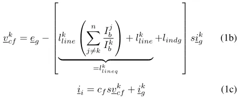
vk =vkcf −lsik (1a)
vkcf =eg−
lkline
n X
j6=k Ibj Ik b
+l k line
| {z }
=lk
lineq
+lindg
sikg (1b)
ii=cfsvkcf+i k
g (1c)
The variables in per unit values are underlined: vk is the
converter-side voltage of the parallel converterk in per unit,
ikcf the LCL-filter capacitor current of the parallel converter
k in per unit,vkcf LCL-filter capacitor voltage of the parallel converterkin per unit, andikg is the grid-side inductor current of the parallel converter k in per unit. The parameters in per unit are in lower case: l is the converter-side inductor inductance in per unit,cf theLCL-filter capacitor capacitance
in per unit,lindgthe grid-side inductor inductance in per unit, lk
line the line-inductance expressed in per unit values using the
bases Vb and Ibk, andeg the grid voltage in per unit. Finally s is the Laplace variable. It is also assumed that all the n
parallel inverters have the same controllerc(s)and the same current reference per uniti∗ so that:
vk=c(s)(i∗−ik) (2)
By analyzing (1), it can be seen that the parallel inverters behave as if they were connected to an equivalent line-inductancelk
lineq equal to the line-inductance weighed by the
rated currentsIk
b. The assumptions for the previous derivations
do not consider that the switching frequency changes for different rated powers in converters so that the controllers and the parameters per unit will not be exactly the same. However, (1) gives insight into the relative influence of other parallel inverters and their rated power in the equivalent line-inductance lk
lineq as seen by the individual parallel inverter.
If the base currents are exactly the same for all the parallel converters Ibk =Ib ∀k, then the overall line-inductance is n
times the grid-inductance llineqk =nlline as demonstrated by
Agorreta et al. in [28].
B. Pad´e Approximant for Filters
Neglecting all the equivalent series resistances of theLCL -filter inductors and capacitor, the transfer function relating the inverter currenti and voltagev is:
GLCL(s) = i
v =
1
Ls
s2+ω2 zLC s2+ω2
res
(3)
with ω2
zLC = (LgCf)−1 is the double zero of the transfer
function and the ω2
res = Ltω2zLC/L the double pole. The
resonance frequency isfres=ωres/(2π)[29].
In the double update mode [30], the sampling frequencyfs
is twice the switching frequencyfs= 2fsw and it may result
ωgLt PI
id
id
PI
iq
*
Lag FilterLag Filter Filter Notch/Lag
Lag FilterLag Filter DAMPING
ACTIVE
ud
ud
vsud
vd
vq
*
*
iq*
Filter Notch/Lag
ωgLt
PI
v*dc
vdc
PI q*
q PLL
vsu ωg
vsuq
[image:4.612.52.299.58.183.2]Lt=L+Lg
Fig. 3: Current control of the LCL-filter based three-phase inverter
with active damping based on notch-filter/lag-filter.
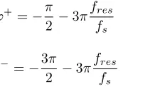
angles of the resonance frequency are separated by 180 degrees and their values are [31]:
ϕ+=−π
2 −3π
fres fs
(4a)
ϕ−=−3π 2 −3π
fres fs
(4b)
wherefres is the resonance frequency. The anglesϕ+andϕ−
are shown in the Bode plot of Fig. 8.
Fig. 3 shows the overall control of the LCL-filter based three-phase inverter. The voltage-vector oriented controller uses a PLL to detect the grid frequencyωg. The direct current id is aligned with the voltage vector and it is varied to
control the active power [32]. The quadrature current iq is
perpendicular to the voltage vector and it is varied to control the reactive power. The inner controllers regulate the direct
d and the quadrature q currents. The outer controller that regulates the DC-link voltage vdc has the i∗d as output. The
outer controller that regulates the reactive q has the i∗q as output. This latter controller is optional and alternatively, i∗q
can be set to zero for unity power factor.
The proposed damping procedures consists of a transfer function located after the PI controller output and before the input to the PWM modulator. This transfer function affects the low-frequency behaviour of the plant and needs to be considered in the tuning procedure of the PI controllers (this is explained in the following Subsection II-C). The bandwidth of the current-control must be lower than the resonance frequency in order to avoid interference [29], [33].
The Pad´e approximant pN,M(s) consists in a quotient of
two polynomials with degree N and M in the numerator and denominator, respectively [34]. The Pad´e approximant
pN,M(s) has the same Taylor series expansion as the
func-tion f(s) up to degree N +P. The Pad´e approximant has been employed to approximate the low frequency behavior of transfer functions in [18], [35]. As the optimum criteria for tuning the PI controllers assumes the presence of first order systems with a single time constant, the Pad´e approximant
p0,1(s)will be considered:
p0,1(s) = 1
τP ade´s+ 1
|p0,1(0) =f(0)andp00,1(0) =f0(0)
(5) The resulting Pad´e approximant p0,1(s) has the same
be-haviour for the low frequency, around s = ωj = 0, as the functionf(s).
C. Tuning Procedure for the Current Controller
The PI controller is tuned by using the low-frequency model of an LCL-filter, which results from neglecting the capacitor branch [18], [29]. The resulting low-frequency model is a simple L-filter with total inductance Lt = L+Lg and the
total resistanceRt=R+Rg. A common procedure for tuning
the current-loop is the technical optimum criterion [32], [36], [37]. This method deals with a transfer function comprising two first order systems:
Glf(s) =
K
(τ s+ 1)(T s+ 1) (6)
with the time constants so that T >> τ andK being a gain. In (6), the large time constant is T =Lt/Rt and the smaller
time constant combines the computational delay (a complete sampling cycle), the PWM delay (approximated as a half of a sampling cycle) and the time constant resulting from the Pad´e approximant of the transfer functions that provide active damping (notch-filter or lag-filters as explained later),
τ=Tcomp+TP W M +τP ade´=Ts+ 0.5Ts+τP ade´ (7)
According to the technical optimum criterion, the integra-tion time cancels the large time constant Ti = T and the
proportional gain is set so to have 4% overshoot (so that the closed-loop transfer-function is a second-order system with
ξ = 0.707 [32], a Butterworth filter with maximally flat magnitude as it corresponds to the technical optimum criterion [37]) :
Kp=
Lt
2τ (8)
The resulting control bandwidth when using the technical optimum criterion for the PI controllers is [32]:
fbw= 1
2π
K
p Lt
= 1
2π
1
2τ (9)
The control bandwidth when no active damping is included (τP ade´= 0in (7)) results as follows:
fbwmax=
1 2π
1 3Ts
(10)
The presence of the transfer functions for active damping results in a bandwidth reduction because of the additional small time constant τP ade´ in τ (7). The control bandwidth when the active damping procedure is included results as follows
fbwτ = 1
2π
1
3Ts+ 2τP ad´e
[image:4.612.136.252.271.332.2]The bandwidth reduction can be calculated by dividing (10) and (11) and it results as follows:
fbwmax fτ
bw
= 1 + τP ade´ 1.5Ts
(12)
However, the total inductance of the LCL-filter is smaller than the inductance required for an L-filter and so lower is the voltage drop. This allows lower saturation levels in the controllers during transients due to the limited DC-link voltage ceiling.
III. NEWTUNINGPROCEDURE FOR THENOTCH-FILTER
This section explains a proposed new tuning procedure for the notch filter, which results in increased stability for line-inductance variations to meet requirement 3).
The notch-filter has a narrow notch at the resonance fre-quency that prevents the excitation of theLCL-filter resonance. In [22], it was proposed to usennotch filters in series in order to increase the width of the notch for increased robustness:
Nn(s) =
s2+ 2D
zωnfs+ω2nf
s2+ 2D
pωnfs+ω2nf !nf
(13)
whereωnf is the notch frequency,DzandDpare the damping
factors for the complex conjugates poles and zeros respectively and nf is the number of sections. The Pad´e approximant pn0,1(s)of the notch-filter is:
pn0,1(s) =
1
2Dp−Dz ωnf s+ 1
nf
≈ 1
2nf Dp−Dz
ωres s+ 1 (14)
Therefore, the resulting delay to be considered in the tuning of the PI controllers is:
τP ade´(notch)= 2nf ωres
(Dp−Dz) (15)
The valuenf = 2was deemed reasonable in terms of proper
trade-off between notch width and computational load [22]. A tolerable bandwidth reduction can be between a half or a third, which results from selecting τP ad´e(noth) between 1.5Ts and 3Ts.
The notch frequency corresponds to the resonance frequency
ωn=ωres. In [22], the damping factorDzwas selected to be
zero as absolutely no component at the resonance frequency is allowed to pass through the PWM modulators. However, this criterion can be relaxed as there is always some parasitic resistance in the LCL-filter. For fs/fres > 2 by fulfilling
the Nyquist frequency limit, the phase around the resonance frequency crosses −π as ϕ+ > −π > ϕ− according to (4). Hence, the resonance frequency is very close to the gain margin crossover frequency and the notch-filter should reduce the amplitude peak so the gain margin is positive:
|CP I(jωres)||Gpd(jωres)||Nn(jωres)|<0.1 (GM ≈ 20 dB)
(16)
where Gpd(s) is the transfer function relating the inverter
voltagev and current i including all the known values (or at least a lower bound) of parasitic resistive elements (inductor resistance and capacitor filter ESR) andCP I(s)is the transfer
function of the PI controller. A proper gain margin (GM) should be higher than 6 dB [38] and selecting 20 dB resulted in good robustness to line-inductance variations. The condition for stability is as follows:
|CP I(jωres)||Gpd(jωres)|
D z Dp
nf
<0.1 (GM ≈ 20 dB)
(17) This relaxation in selecting Dz results in a wider notch,
which will increase the stability against the line-inductance variation. The Tustin rule with pre-warping at the resonance frequency reduces the notch width of the discretized filter. The matchedz-transform method [39] results in a notch width closer to that of the continuous case, provided the extra reduction in gain and extra phase delay still fulfills the stability conditions.
This notch filter solution requires the resistances of the inductors to be known. There is usually no control over these parameters when designing the LCL-filter. If there is an upgrade in the inductors, the inductance will be the same but the resistance may be different (and probably lower). In addition, the resistance of the inductors varies with the temperature. Hence, a lower bound of the resistance of the inductors is necessary to apply this active damping procedure.
IV. NOVELACTIVEDAMPINGPROCEDUREUSING LAG-FILTERS
This section explains a novel procedure for active damping based on lag-filters that fulfils the conditions stated for the target application without requiring to know the resistance of the inductors.
The proposed method uses lag-filtersGnlag(s)to include an
additional phase lag is availableϕat the resonance frequency, so that the new phase angles at the resonance frequency are:
ϕ0+=ϕ++ϕ (18a)
ϕ0−=ϕ−+ϕ (18b)
These angles are illustrated in Fig. 8. The values of ϕ
required to achieve stability can be inferred from the encir-clements of −1 using the Nyquist criterion. However, the stability condition is easier to infer by considering that there should be a positive real part at the resonance frequency (resistive behavior <{Gnlag(jωres)Gud(jωres)} > 0). The
phase angle at the resonance frequency is as follows:
ϕres=
ϕ0++ϕ0−
2 +ϕ=−π−3π
fres fs
+ϕ (19)
and the necessary condition for stability is −π/2 < ϕres < π/2. Therefore, the phase delay required for stability is:
−3π
2 + 3π
fres fs
< ϕ <−5π 2 + 3π
fres fs
Multiples of2πhave been added to (20) in order to derive the stability condition. If ϕres = 0 as in [40], the value
of Gnlag(jωres)Gud(jωres) is real so the behavior at the
resonance frequency is purely resistive.
In order to produce the required phase delay at the resonance frequency, the proposed lag-filter uses lead-lag (zero-pole) sections. The net result is a lag compensator [38] but the zero alleviates the phase-lag at lower frequencies and so the bandwidth reduction. The number of first-order lag-filters is
nl and each section will produce a phase delay ϕi=ϕ/nl:
Gnlag(s) = s ωresr+ 1
rs ωres + 1
!nl
(21)
with
r=
s
1−sin(ϕi) 1 + sin(ϕi)
(22)
The resulting sections are discretized by using the Tustin method with pre-warping at the resonance frequency in order to preserve the desired characteristics in the discrete domain at the resonance frequency. Each lag section has unit amplitude at DC and a gain reduction ofr2in the high-frequency region. The Pad´e approximant pn0,1(s)of the lag-filters is:
pn0,1(s) = "
1 1 ωres r−
1 r
s+ 1 #nl
≈ n 1
l ωres r−
1 r
s+ 1 (23)
Therefore, the resulting delay to be considered in the tuning of the PI controllers is:
τP ade´(nlag)=
nl ωres
r−1
r
(24)
The number of lag-filters nl must result in |ϕi| < π/2.
For a fixed value of ϕ, a higher number of sections nl
results in a smaller delay in (24) because the term depending on r (22) decays faster than nl. Therefore, increasing the
number of sections nl will increase bandwidth by reducing
(24). However, these improvements are at the expense of more computations. Making nl = 4 results in approximately the
same number of computations as in the previous second order notch filter and it provides a reasonable trade-off between bandwidth reduction and processing time.
The phase margin P M in degrees is related to the phase delay ϕas follows (see Figs. 5 and 8):
ϕ= (P M−180)2π
360+
−3π
2 + 3π
fres fs
(25)
This formula can be used to select the PM for the nomi-nal resonance frequency. However, the increase in the line-inductance Ll and the increase of the number of parallel
inverters increases the grid inductance Lg and reduces the
resonance frequencyfres. The proper tuning procedure should
[image:6.612.339.532.83.231.2]consider a minimum adequate P M (between 30 and 60
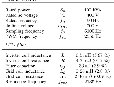
TABLE I: Parameters of the set-up used for simulations and experi-ments.
Grid-tie inverter
Rated power Sn 100 kVA Rated ac voltage Vn 400 V Rated frequency fn 50 Hz dc link voltage vDC 700 V Sampling frequency fs 5100 Hz PWM frequency fsw 2550 Hz
LCL-filter
Inverter coil inductance L 0.5 mH(5.67 %) Inverter coil resistance R 4.7 mΩ(0.17 %) Filter capacitor Cf 33µF(2.9 %) Grid coil inductance Lg 0.25 mH(2.8 %) Grid coil resistance Rg 2.36 mΩ(0.09 %) Resonance frequency fres 2135 Hz
degrees [38]) for the maximum realistic increase in the line-inductance which results in the minimum resonant frequency
fmin
res . The prover value forϕis calculated by substituting the
selected P M for the minimum resonance frequency in (25), yet the system must have a reasonableP M for the nominal resonance frequency. If the resulting P M for the nominal resonance frequency is too small, the worst condition fmin res
cannot be fulfilled and theP M should be increased.
V. SIMULATIONRESULTS
Table I shows all the data of the set-up used for simulations and experiments. The design procedure for the LCL-filter design is explained in [29]. The ratioLg/L= 1.6was selected
in [29], but in this manuscript the value of the grid-side inductance Lg is varied from an initial value of 0.25 mH
(Lg/L = 0.5) to a final value of 2.5 mH (Lg/L = 5) in
order to study the variations in the line-inductance. The simu-lation software is Matlab/Simulink/SimPowerSystems and the semiconductor switches are ideal. The values of the LCL -filter parameters presented in Table I result from applying the design procedure explained in [29]. The experiments will be performed in a scaled 100 kVA three-level NPC converter whereas the target industrial application uses an 800 kVA two-level converter. The voltage is measured at the filter capacitor terminals and is used for grid synchronization. For the initial value ofLg, the ratio betweenfs/fres= 2.4is very close to
the Nyquist limit. In addition, sudden increments in the grid inductance will be considered that may be due to additional line-inductance or due to the connection of additional parallel inverters [28]. In both situations, achieving stability is a challenging task for the active damping procedure.
A. New Tuning Procedure for the Notch-filter
Previous references [18], [22] considered a bandwidth re-duction of no more than 2 when using active damping. A bandwidth reduction of 2.64 times was selected for the notch-filter procedure; simulations and experiments will show that the resulting bandwidth was sufficient for tracking the sinusoidal reference in the current-loop. Solving (12) results in
τP ade´(notch)= 2.46Ts. The required parameters of the
notch-filter Dp = 1.7 andDz = 8.86e−2 are calculated by using
-60 -40 -20 0
M
agni
tude
(dB)
Continous Notch-filter Low Frequency Model Discrete Notch-filter (Tustin) Discrete Notch-filter (Matched)
102 103
-180 -90 0 90 180
P
ha
se
(de
g)
[image:7.612.329.544.53.254.2]Frequency (Hz)
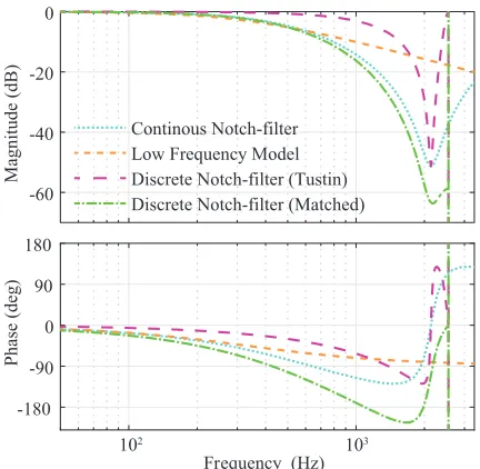
Fig. 4: Frequency response of the continuous notch-filter, the discrete notch-filter using the Tustin rule with pre-warping at the resonance
frequency and the discrete notch-filter using the matchedz-transform
[image:7.612.67.283.55.266.2]rule.
Fig. 5 shows the Bode plot for the open-loop transfer function with no notch-filter (no active damping procedure), the notch-filter using the Tustin rule and the notch-filter using the matchedz-transform rule. It can be seen that the system is unstable when no notch-filter (no active damping procedure) is included. The overall system is stable when the notch-filter using the Tustin rule is included. The gain margin crossover frequency is still approximately at the resonance frequency (as explained in Section III) and the gain margin is positive rendering the overall system stable. The overall system is also stable when the notch-filter uses the matched z-transform and it has a wider notch. This will result in increased robustness against resonance frequency variations due to changing line-impedance. Fig. 5 also shows the Bode plot for the low-frequency model that neglects the LCL-filter branch capacitor and uses the Pad´e approximant of the notch-filter, which is very close to the exact model in the low-frequency region.
The minimum GM and PM are also shown in Fig. 5. It can be seen that the control-loop is unstable when the active damping procedure is not present with negative GM at the resonance frequency. After including the notch filter, the GM at the resonance frequency is positive and 23.7 dB; close to the selected 20 dB in (17). The minimum GM and PM are respectively 11.4 dB and 52.4 degrees for the case using the Tustin rule. For the case of the z-transform matched rule, the minimum GM and PM are respectively 5.8 dB and 28.7 degrees. The minimum stability margins are lower for the z-transform matched rule, but still around the recommended 6 dB and 30 degrees [38].
B. Novel Active Damping Procedure based on Lag-filters
For the multiple lag-filters, a phase margin P M = 30 degrees is considered adequate when the grid inductance Lg
-100 -50 0
M
agni
tude
(dB)
102 103
-450 -360 -270 -180 -90
P
ha
se
(de
g
)
Frequency (Hz) PM: 52.4⁰
PM: 52.4⁰
PM: 61.5⁰
PM: 61.5⁰
PM: 28.7⁰
PM: 28.7⁰
fres=
fres=2135 Hz2135 Hz
No Active Damping
No Active Damping
PM: 44.2⁰
PM: 44.2⁰
GM: 14.7 dB
GM: 14.7 dB
GM: 5.8 dB
GM: 5.8 dB
GM: -28.1 dB
GM: -28.1 dB
GM: 23.7 dB
GM: 23.7 dB
GM: 11.4 dB
GM: 11.4 dB
Discrete Notch-filter (Tustin)
Discrete Notch-filter (Tustin)
Discrete Notch-filter (Matched)
Discrete Notch-filter (Matched)
Low-frequency Model
Low-frequency Model
Fig. 5: Bode plot for the open-loop transfer function with no notch-filter (no active damping procedure), the notch-filter using the
Tustin rule and the notch-filter using the matched z-transform rule.
The figure also shows the open-loop transfer function for the low-frequency model.
0 0.005 0.01 0.015 0.02 0.025
0 0.5 1
t
pu
Exact Model
Low Freq. and Padé Aprox
Fig. 6: Step response of the exact model and approximate model
using theLCL-filter low-frequency model and the Pad´e approximant
of the lag-filters.
is nine times the initial value (this situation corresponds to the minimum resonance frequency fmin
res = 1362.9 Hz). This
results in ϕ = −155.7 degrees by substituting in (25) and
ϕi=−38.9degrees (r= 2.09according to (22)) by selecting nl= 4in order to have the same number of computations as
in the notch-filter case.
The resulting delay τP ade´(nlag) = 2.46Ts is calculated
with (24) and entails an acceptable bandwidth reduction of 2.6 times (same as in the notch-filter case). For this case as well it is required to use the low-frequency model that neglects the LCL-filter capacitor branch and uses the Pad´e approximant of the lag-filters in order to tune the PI controllers according to (8). Fig. 6 compares the step responses of the exact model and the low-frequency model that neglects the
[image:7.612.333.545.326.435.2]-50 -40 -30 -20 -10 0
M
agni
tude
(dB)
Continuous Lag-filters Discrete Lag-filters (Tustin)
102 103
-180 -135 -90 -45 0
P
ha
se
(de
g)
[image:8.612.330.542.53.255.2]Frequency (Hz)
[image:8.612.86.263.56.227.2]Fig. 7: Frequency response of the continuous lag-filters and the discrete lag-filters using the Tustin rule with pre-warping at the resonance frequency.
Fig. 7 shows the frequency response of the continuous lag-filters and the discrete lag-lag-filters using the Tustin rule with pre-warping at the resonance frequency. There is an exact match between the discrete and continuous models around the resonance frequency as expected. Unlike the notch-filter case, the discrete lag-filters do not result in an estimable width reduction.
Fig. 8 shows the Bode plot for the open-loop transfer function with no lag-filters (no active damping procedure) and the lag-filters using the Tustin rule. It can be seen that the system is unstable when no lag-filters (no active damping procedure) are included. When the lag-filters are inserted, the overall system is stable and the selection ofP M = 30degrees for the maximum grid inductance was adequate. Fig. 8 also shows the Bode plot for the low-frequency model that neglects theLCL-filter branch capacitor and uses the Pad´e approximant of the notch-filter, which is very close to the exact model in the low-frequency region. The minimum GM and PM are also shown in Fig. 8. The control-loop is unstable when the active damping procedure is not present with negative GM at the resonance frequency. The minimum GM and PM are respectively 6.69 dB and 32 degrees, slightly higher than the recommended 6 dB and 30 degrees [38].
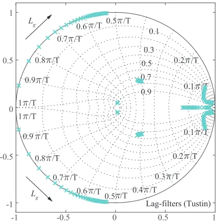
Fig. 9 shows the root locus in the z-plane when varying
Lg from 75% to 1000% of the initial value (from 0.2 mH to
2.5 mH) for the case of the lag-filters. The overall system is stable for the whole range of Lg variation around the initial
value. This is because the design procedure considered the stability for the worst case with P M = 30degrees when the grid inductance Lg is nine times the initial value.
Fig. 10 shows the simulation results for the notch-filter case using the z-plane. The only parasitic resistances considered are R and Rg, the extra line-inductance is purely inductive.
The current-loop cannot be stable by the passive damping provided by these limited resistance values and active damping is required. The current-loop is stable for all the situations, but the system resonates for the initial inductance value of
-100 -50 0
M
agni
tude
(dB)
102 103
-450 -360 -270 -180 -90
P
ha
se
(de
g)
Frequency (Hz)
ϕ
+ϕ
+ϕ
−ϕ
−ϕ
’
+=ϕ
++ϕ
ϕ
’
+=ϕ
++ϕ
ϕ
’
−=ϕ
−+ϕ
ϕ
’
−=ϕ
−+ϕ
PM: 61.5⁰
PM: 61.5⁰
fres=
fres=2135 Hz2135 Hz
Low-frequency Model
Low-frequency Model
PM: 32⁰
PM: 32⁰
GM: -28.1 dB
GM: -28.1 dB
GM: 6.69 dB
GM: 6.69 dB
GM: 14.4 dB
GM: 14.4 dB
Discrete Lag-filters
Discrete Lag-filters
No Active Damping
[image:8.612.331.544.316.534.2]No Active Damping
Fig. 8: Bode plot for the open-loop transfer function with no lag-filters (no active damping procedure) and the lag-lag-filters for active damping. The figure also shows the open-loop transfer function for the low-frequency model.
-1 -0.5 0 0.5 1
-1 -0.5 0 0.5 1
0.9 0.7 0.5 0.3
0.1
1 /T
0.9 /T
0.8 /T
0.7 /T 0.6 /T
0.5 /T 0.4 /T 0.3 /T
0.2 /T 0.1 /T 1 /T
0.9 /T 0.8 /T
0.7 /T
0.6 /T 0.5 /T
0.2 /T
0.1 /T
Lag-filters (Tustin) Lg
Lg
Fig. 9: root locus in thez-plane when varyingLgfrom 80% to 1000%
(from 0.2 mH to 2.5 mH) for the lag-filter using the Tustin rule with pre-warping.
Lg. This is because the sampling frequency is very close (2.4
times) to the resonance frequency and the achieved damping is not sufficient. Active damping algorithms usually require that the sampling frequency be more than 3 times the resonance frequency [41]. After three cycles, an extra inductance of 9 times the initial inductance Lg (2.25 mH) is connected
0 0.05 0.1 0.15 0.2
t (s)
pu
Disconnect Active Damping
Increase 9Lg
THD=52%
THD=0.47%
[image:9.612.320.558.56.298.2]Converter Current Grid Current Capacitor Voltage
Fig. 10: Simulation results for the lag-filters using the Tustin rule with pre-warping.
Finally, it should be mentioned that unsuccessful attempts were made to use well-established procedures for active damp-ing [41]. This remarks that the proposed procedures were successful in the face of difficult conditions to achieve stability with the LCL-filter based three-phase NPC inverter using the parameters shown in Table I.
VI. EXPERIMENTALRESULTS
Fig. 11 shows a picture of the 100 kVA set-up used for the experiments. The three-level NPC grid-tie inverter is directly connected to a Regatron programmable three-phase power supply. The initial value of the grid inductance Lg is 0.25
mH (Lg = 0.5L) and during the tests the grid inductance is
increased up to 0.75 mH in a first step and up to 1.25 mH (Lg= 2.5L) in a second step. The grid inductance increments
are sudden by opening the bypass breakers that short-circuit extra inductors.
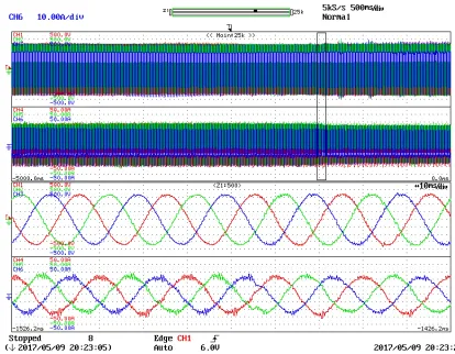
Figs. 12-14 show the oscilloscope captures when the active damping procedure based on lag-filters is connected. Fig. 12 shows the grid voltage and the current waveforms after a 25 Amp step change in the current reference. The response is critically damped and consistent with the simulation shown in Fig. 6. The system behavior is stable but the current exhibits a large ripple because the switching frequency is very close (1.2 times) to the resonance frequency. The experiments are fully consistent with the simulations shown in Fig. 10. Fig. 13 shows the grid voltage and current waveforms for the sudden addition of extra line-inductance with a value twice the initial value of Lg (0.5 mH). At the beginning of this experiment,
General Breaker (operated manually)
General Breaker (operated manually)
Main Contactor Main Contactor
Auxiliar Rectifier Auxiliar Rectifier
Signal Acquisition Signal Acquisition
LCL-Filter LCL-Filter
IGBT Drivers IGBT Drivers
Grid-tie NPC Inverter
Grid-tie NPC Inverter
Machine=side NPC Inverter Machine=side NPC Inverter
[image:9.612.72.283.61.340.2]Sensors Sensors
Fig. 11: 100 kVA Experimental set-up.
Fig. 12: Experimental results for the lag-filters: grid voltage and current waveforms for a 25 Amp current reference step.
the grid inductance Lg has its the initial value (0.25 mH).
After adding the extra line-inductance, the grid inductance
Lg is three times its initial value (0.75 mH). The system
remains stable and the current harmonics are reduced due to the filtering capability of the additional inductance. Finally, Fig. 14 shows the grid voltage and current waveforms for another sudden addition of extra line-inductance with a value twice the initial value ofLg(0.5 mH). At the beginning of this
experiment, the grid inductance is three times its initial value of Lg (0.75 mH). After adding another extra line-inductance,
the grid inductance Lg is five times the initial value (1.25
mH). The system remains stable with a grid inductance Lg
of 5 times its initial value (1.25 mH), which demonstrates the robustness against line-inductance variations of the proposed novel active damping procedure based on lag-filters.
Fig. 13: Experimental results for the lag-filters: grid voltage and current waveforms for the sudden addition of extra line-inductance
with a value twice the initial value ofLg(0.5 mH). At the beginning
of this experiment, the grid inductance has its the initial value Lg
(0.25 mH). After adding the extra line-inductance, the grid inductance
Lg is three times its initial value (0.75 mH).
Fig. 14: Experimental results for the lag-filters: grid voltage and current waveforms for the sudden addition of another extra
line-inductance with a value twice the initial value ofLg(0.5 mH). At the
beginning of this experiment, the grid inductanceLgis three times its
initial value (0.75 mH). After adding another extra line-inductance,
the grid inductanceLg is five times its initial value (1.25 mH).
additional damping because of the non-modeled dissipative elements (cores losses, capacitor ESR, inverter losses,...).
VII. DISCUSSION
The numerous requirements stated for this industrial appli-cation are very constraining and the procedure presents limi-tations and trade-offs in the results. The maximum bandwidth
fmax
bw is determined by (10) and the switching frequency is the
limiting factor. The switching frequency is limited in medium voltage converters so to reduce the switching losses in the semiconductors. The proposed procedures allow selecting the amount of bandwidth to be sacrificed for using active damping; the final bandwidth fbwτ is determined by (12). In this case, the trade-off is between bandwidth reduction and robustness to line-inductance variations. The bandwidth of the current-controllers must be sufficient to track the sinusoidal reference and, in certain cases, to cancel a specific harmonic component
as for example if there is substantial harmonic content in the grid voltage.
The main disadvantage of the procedure is that the damping many not be sufficient for very low values of Lg/L. Even
though the current-loop is stable for all range ofLg variation,
the system resonates in the simulation results for the initial
Lg with the sampling frequency is very close (2.4 times) to
the resonance frequency. However, the system will never work with the initial inductance valueLg= 0.25mH (Lg/L= 0.5)
as that the wind-turbine manufacturer assumes some known values for the line-impedance in order to minimize the grid-side inductor size. The system achieved a THD<5% forLg= 0.9L (Lg = 0.45mH, 1.8 times the initial value of Lg). For
the ratio Lg/L= 1.6 as selected in [29], the THD achieved
is 1.57%.
The results in the simulations and experiments for the notch-filter (using the z-transform matched rule) are very similar to those of the lag-filter. The root locus analysis in the z-plane shows that the system is stable for the whole range for Lg
varying from 80% to 1000%. In the simulation results, the systems initially resonated with THD=52% with the sampling frequency is very close (2.4 times) to the resonance frequency and finally it achieves a THD=0.47% after applying 9 times the initial inductance Lg (2.25 mH). The system achieves a
THD<5% forLg/L= 0.8(Lg=0.4 mH, 1.6 times the initial
value of Lg). For the ratio Lg/L= 1.6 as selected in [29],
the THD achieved is 1.53%. The main disadvantage of this the notch filter procedure is the necessity of knowing the resistance of the inductors.
VIII. CONCLUSION
This paper present a list of requirements for active damping inLCL-filter based medium-voltage grid-tie parallel inverters. The proposed solutions use filters in the voltage reference to the modulator. The presented approach allows selecting the bandwidth to be sacrificed for using active damping by calculating the Pad´e aproximant. The proposed tuning procedure for the notch-filter increases the robustness against the line-impedance variations using a simple design procedure that that requires to know the resistance of the inductors. The method of the lag-filters selects the phase margin for the worst case increase in the grid inductance to guarantee stability. Therefore, this proposed procedure constitutes an appropriate solution for this industrial application related to wind energy.
REFERENCES
[1] R. Pena-Alzola, M. Liserre, F. Blaabjerg, R. Sebastian, J. Dannehl, and F. Fuchs, “Analysis of the passive damping losses in lcl-filter-based grid converters,”IEEE Trans. Power Electron., vol. 28, no. 6, pp. 2642–2646, June 2013.
[2] P. A. Dahono, “A control method to damp oscillation in the input lc filter,” in2002 IEEE 33rd Annu/ IEEE Power Electron. Specialists Conf. Proc. (Cat. No.02CH37289), vol. 4, 2002, pp. 1630–1635.
[image:10.612.66.273.294.455.2][4] ——, “Grid-current-feedback active damping for lcl resonance in grid-connected voltage-source converters,” IEEE Trans. Power Electron., vol. 31, no. 1, pp. 213–223, Jan 2016.
[5] V. Miskovic, V. Blasko, T. M. Jahns, A. H. C. Smith, and C. Romenesko, “Observer-based active damping of lcl resonance in grid-connected voltage source converters,”IEEE Trans. Ind. Applicat., vol. 50, no. 6, pp. 3977–3985, Nov 2014.
[6] Y. Lyu, H. Lin, and Y. Cui, “Stability analysis of digitally controlled lcl-type grid-connected inverter considering the delay effect,”IET Power Electron., vol. 8, no. 9, pp. 1651–1660, 2015.
[7] J. Wang, J. D. Yan, L. Jiang, and J. Zou, “Delay-dependent stability of single-loop controlled grid-connected inverters with lcl filters,”IEEE Trans. Power Electron., vol. 31, no. 1, pp. 743–757, Jan 2016. [8] C. Chen, J. Xiong, Z. Wan, J. Lei, and K. Zhang, “A time delay
compensation method based on area equivalence for active damping of an lcl -type converter,”IEEE Trans. Power Electron., vol. 32, no. 1, pp. 762–772, Jan 2017.
[9] R. Guzman, L. G. de Vicua, J. Morales, A. Momeneh, J. Miret, and J. Torres-Martnez, “Active damping based on ackermann’s formula for a three-phase voltage source inverter with lcl filter,” inIECON 2015 -41st Annu. Conf. of the IEEE Ind. Electron. Soc., Nov 2015, pp. 001 217– 001 222.
[10] D. Perez-Estevez, J. Doval-Gandoy, A. G. Yepes, and O. Lopez, “Positive- and negative-sequence current controller with direct discrete-time pole placement for grid-tied converters with lcl filter,”IEEE Trans. Power Electron., vol. PP, no. 99, pp. 1–1, 2016.
[11] F. Huerta, D. Pizarro, S. Cobreces, F. J. Rodriguez, C. Giron, and A. Rodriguez, “Lqg servo controller for the current control of lcl grid-connected voltage-source converters,”IEEE Trans. Ind. Electron., vol. 59, no. 11, pp. 4272–4284, Nov 2012.
[12] J. Roldan-Perez, A. Garcia-Cerrada, J. L. Zamora-Macho, and M. Ochoa-Gimenez, “Helping all generations of photo-voltaic inverters ride-through voltage sags,” IET Power Electron., vol. 7, no. 10, pp. 2555–2563, 2014.
[13] M. Andresen, M. Liserre, F. W. Fuchs, and N. Hoffmann, “Design of a grid adaptive controller for pwm converters with lcl filters,” inIECON 2015 - 41st Annu. Conf. of the IEEE Ind. Electron. Soc., Nov 2015, pp. 003 664–003 671.
[14] J. Kukkola and M. Hinkkanen, “State observer for grid-voltage sensor-less control of a converter equipped with an lcl filter: Direct discrete-time design,”IEEE Trans. Ind. Applicat., vol. 52, no. 4, pp. 3133–3145, July 2016.
[15] H. Komurcugil, S. Ozdemir, I. Sefa, N. Altin, and O. Kukrer, “Sliding-mode control for single-phase grid-connected mboxLCL -filtered vsi with double-band hysteresis scheme,” IEEE Trans. Ind. Electron., vol. 63, no. 2, pp. 864–873, Feb 2016.
[16] R. Guzman, L. G. de Vicuna, J. Morales, M. Castilla, and J. Miret, “Model-based active damping control for three-phase voltage source inverters with lcl filter,”IEEE Trans. Power Electron., vol. PP, no. 99, pp. 1–1, 2016.
[17] J. Dannehl, F. W. Fuchs, S. Hansen, and P. B. Thogersen, “Investigation of active damping approaches for pi-based current control of grid-connected pulse width modulation converters with lcl filters,” IEEE Trans. Ind. Applicat., vol. 46, no. 4, pp. 1509–1517, July 2010. [18] R. Pena-Alzola, M. Liserre, F. Blaabjerg, R. Sebastin, J. Dannehl, and
F. W. Fuchs, “Systematic design of the lead-lag network method for active damping in lcl-filter based three phase converters,”IEEE Trans. Ind. Informat., vol. 10, no. 1, pp. 43–52, Feb 2014.
[19] V. Blasko and V. Kaura, “A novel control to actively damp resonance in input lc filter of a three-phase voltage source converter,”IEEE Trans. on Ind. Applicat., vol. 33, no. 2, pp. 542–550, Mar 1997.
[20] X. Bao, F. Zhuo, Y. Tian, and P. Tan, “Simplified feedback linearization control of three-phase photovoltaic inverter with an lcl filter,” IEEE Trans. Power Electron., vol. 28, no. 6, pp. 2739–2752, June 2013. [21] J. Dannehl, M. Liserre, and F. W. Fuchs, “Filter-based active damping
of voltage source converters with lcl filter,”IEEE Trans. Ind. Electron., vol. 58, no. 8, pp. 3623–3633, Aug 2011.
[22] R. Pena-Alzola, M. Liserre, F. Blaabjerg, M. Ordonez, and T. Kerekes, “A self-commissioning notch filter for active damping in a three-phase lcl -filter-based grid-tie converter,”IEEE Trans. Power Electron., vol. 29, no. 12, pp. 6754–6761, Dec 2014.
[23] W. Yao, Y. Yang, X. Zhang, F. Blaabjerg, and P. C. Loh, “Design and analysis of robust active damping for lcl filters using digital notch filters,” IEEE Trans. Power Electron., vol. 32, no. 3, pp. 2360–2375, March 2017.
[24] J. Y. Hung, “Feedback control with posicast,”IEEE Trans. Ind. Electron., vol. 50, no. 1, pp. 94–99, Feb 2003.
[25] A. Vidal, A. G. Yepes, F. D. Freijedo, . Lpez, J. Malvar, F. Baneira, and J. Doval-Gandoy, “A method for identification of the equivalent inductance and resistance in the plant model of current-controlled grid-tied converters,”IEEE Trans. Power Electron., vol. 30, no. 12, pp. 7245– 7261, Dec 2015.
[26] X. Fu and S. Li, “Control of single-phase grid-connected converters with lcl filters using recurrent neural network and conventional control methods,”IEEE Trans. Power Electron., vol. 31, no. 7, pp. 5354–5364, July 2016.
[27] M. Liserre, A. Dell’Aquila, and F. Blaabjerg, “Genetic algorithm-based design of the active damping for an lcl-filter three-phase active rectifier,” IEEE Trans. Power Electron., vol. 19, no. 1, pp. 76–86, Jan 2004. [28] J. L. Agorreta, M. Borrega, J. Lpez, and L. Marroyo, “Modeling and
control of n -paralleled grid-connected inverters with lcl filter coupled due to grid impedance in pv plants,” IEEE Trans. Power Electron., vol. 26, no. 3, pp. 770–785, March 2011.
[29] M. Liserre, F. Blaabjerg, and S. Hansen, “Design and control of an lcl-filter-based three-phase active rectifier,”IEEE Trans. Ind. Applicat., vol. 41, no. 5, pp. 1281–1291, Sept 2005.
[30] V. Blasko, V. Kaura, and W. Niewiadomski, “Sampling of discontinuous voltage and current signals in electrical drives: a system approach,”IEEE Transactions on Industry Applications, vol. 34, no. 5, pp. 1123–1130, Sep 1998.
[31] Y. Tang, W. Yao, P. C. Loh, and F. Blaabjerg, “Design of lcl filters with lcl resonance frequencies beyond the nyquist frequency for grid-connected converters,”IEEE J. of Emerging and Select. Topics in Power Electron., vol. 4, no. 1, pp. 3–14, March 2016.
[32] V. Blasko and V. Kaura, “A new mathematical model and control of a three-phase ac-dc voltage source converter,”IEEE Trans. Power Electron., vol. 12, no. 1, pp. 116–123, Jan 1997.
[33] M. L. *, F. Blaabjerg, and A. DellAquila, “Step-by-step design proce-dure for a grid-connected three-phase pwm voltage source converter,” International Journal of Electronics, vol. 91, no. 8, pp. 445–460, 2004. [34] W. Yang, W. Cao, T. Chung, and J. Morris,Applied Numerical Methods
Using MATLAB. Wiley, 2005.
[35] R. Pena-Alzola, D. Campos-Gaona, P. F. Ksiazek, and M. Ordonez, “Dc-link control filtering options for torque ripple reduction in low-power wind turbines,”IEEE Trans. Power Electron., vol. 32, no. 6, pp. 4812– 4826, June 2017.
[36] W. Leonhard, Control of Electrical Drives, ser. Engineering library. Springer Berlin Heidelberg, 2001.
[37] J. W. Umland and M. Safiuddin, “Magnitude and symmetric optimum criterion for the design of linear control systems: what is it and how does it compare with the others?”IEEE Trans. Ind. Applicat., vol. 26, no. 3, pp. 489–497, May 1990.
[38] K. Ogata,Modern Control Engineering, ser. Instrumentation and con-trols series. Prentice Hall, 2010.
[39] E.-K. Press, G. Franklin, J. Powell, and M. Workman,Digital Control of Dynamic Systems. Ellis-Kagle Press, 1998.
[40] J. Roldan-Perez, E. Bueno, and A. Rodriguez-Cabero, “A simplified active damping method for grid-connected converters with lcl filters,” inIEEE Energy Conversion Congr. and Expo. ECCE’ 2017, 2017. [41] R. Pena-Alzola, M. Liserre, F. Blaabjerg, M. Ordonez, and Y. Yang,
“Lcl-filter design for robust active damping in grid-connected convert-ers,” IEEE Trans. Ind. Informat., vol. 10, no. 4, pp. 2192–2203, Nov 2014.
Rafael Pe ˜na AlzolaRafael Pe˜na-Alzola received the
Since June 2017, he is Research Fellow at the Rolls Royce University Technology Centre at the University of Strathclyde in Glasgow, UK. His research interests are energy storage, LCL-filters, solid-state transformers, power electronics for hybrid electric aircraft and innovative control techniques for power converters.
Javier Rold´an-P´erezJavier Rold´an-P´erez received a
B.S. degree in industrial engineering, a M.S. degree in electronics and control systems, a M.S. degree in system modeling, and a Ph.D. degree in power electronics, all from Comillas Pontifical University, Madrid, in 2009, 2010, 2011, and 2015, respectively. From 2010 to 2015, he was with the Institute for Research in Technology (IIT), Comillas University. In 2014, he was a visiting Ph.D. student at the Department of Energy Technology, Aalborg Univer-sity, Denmark. From 2015 to 2016 he was with the Electric and Control Systems Department at Norvento Energa Distribuida. In September 2016 he joined the Electrical Systems Unit at IMDEA Energy Institute, where his research topics are the integration of renewable energies, microgrids, and power electronics applications.
Emilio Bueno Emilio J. Bueno (S’05-M’06) was
born in Madrid, Spain, in 1972. He received the M.S. and Ph.D. degrees in electronics engineering from the University of Alcal´a, Alcal´a de Henares, Spain, in 1999 and 2005, respectively. Since 2009, he has been an Associate Professor with the Department of Electronics, University of Alcal´a, and a member of the Electronics Engineering Applied to Renewable Energies Research Group.
From 2010 to 2013, he was a Vice-Dean of the Polytechnic School, University of Alcal´a, in charge of electrical engineering studies. His research interests include linear control of grid converters and drives, power quality, distributed generation systems, and medium-voltage converter topologies.
Francisco Huerta Francisco Huerta (S’08-M’11)
received the M.Sc. degree and the Ph.D. degree in electronics engineering from the University of Alcal´a, Alcal´a de Henares, Spain, in 2006 and 2011, respectively.
He worked as a Research Assistant from 2007 and 2012 with the University of Alcal´a. From 2013 until 2016, he was a Postdoctoral Researcher with Institute IMDEA Energy. From 2016 to 2017, he worked as a Researcher with the University of Alcal´a. Currently he is an Assistant Professor with the Carlos III University of Madrid. His research interests include control of power electronics converters, power quality and distributed power generation systems.
David Campos-Gaona David Campos-Gaona
(M’12) received the B.E. degree in electronic engineering, and the M.Sc. and Ph.D. degrees in electrical engineering, all from Instituto Tecnolgico de Morelia, Morelia, Mexico, in 2004, 2007, and 2012, respectively. From 2014 to 2016, he was a Postdoctoral Research Fellow with the Department of Electrical and Computer Engineering, University of British Columbia, Vancouver, Canada. Since August 2016, he is a Research Associate with the University of Strathclyde, Glasgow, U. K. His research interest include wind farm power integration, HVDC transmission systems, and real-time digital control of power-electronic-based devices.
Marco LiserreMarco Liserre
(S’00-M’02-SM’07-F’13) received the MSc and PhD degree in Electrical Engineering from the Bari Polytechnic, respectively in 1998 and 2002. He has been Associate Professor at Bari Polytechnic and Professor at Aalborg Univer-sity (Denmark). He is currently Full Professor and he holds the Chair of Power Electronics at Christian-Albrechts-University of Kiel (Germany). He has published over 300 technical papers (more than 100 of them in international peer-reviewed journals) and a book. These works have received more than 20,000 citations. Marco Liserre is listed in ISI Thomson report The worlds most influential scientific minds. He is member of IAS, PELS, PES and IES. He has been serving all these societies in different capacities and he has received several IEEE awards.
Graeme Burt Graeme M. Burt (M’95) received