Compressively-strained, buried-channel Si
0
.
7
Ge
0
.
3
p-MOSFETs fabricated on SiGe virtual substrates
using a 0.25
µ
m CMOS process
Matthew P. Temple, Douglas J. Paul, Member, IEEE,, Yue T. Tang, Andrew M. Waite, Claudia Cerrina,
Alan G.R. Evans, Xiaobing Li, Jing Zhang, Sarah H. Olsen and Anthony G. O’Neill
Abstract— Enhanced performance is demonstrated from a
buried, compressively strained-Si0.7Ge0.3 p-MOSFET fabricated
on a relaxed Si0.85Ge0.15 using a high thermal budget 0.25 µm
CMOS process. The devices are designed to be fully compatible with a strained-Si CMOS process but offers a number of potential benefits over a surface channel p-MOSFET for certain circuit applications. Transconductance, on-current, hole velocity and mobility enhancements are observed over surface strained-Si channel devices on both Si0.85Ge0.15 and Si0.8Ge0.2 virtual
substrates and the bulk Si control devices for constant effective channel length. The buried channel devices exhibit enhancements over the Si control devices of 93% in on-current and 62% in hole velocity for 0.25 µm effective channel length devices without
compromising the subthreshold characteristics. The extracted effective mobility for the buried channel device is over 40% greater than the universal mobility curve for bulk Si p-MOS devices at 0.55 MV/cm vertical effective electric fields.
Index Terms— CMOS, p-MOSFET, strained-Si, SiGe, quantum
well, thermal budget, drain current enhancements, transconduc-tance enhancements, virtual substrate.
I. INTRODUCTION
SiGe in the form of the heterojunction bipolar transistor became a main stream technology in 1999 with the sales of the first circuits using the technology [1][2]. While the share of SiGe devices has been increasing even during the microelectronics market downturn in the last few years, it is complementary metal oxide semiconductor (CMOS) technol-ogy which has the largest share of the microelectronics market [3]. CMOS devices are now being aggressively scaled to gate-lengths below 100 nm and predictions suggest that the scaling is likely to continue for at least another decade [3]. A number of problems, however, are being found as the MOSFET gate-lengths are reduced. In particular the gate oxide thickness in state-of-the-art production devices is now below 2 nm and thinner oxides increase the off-state current through the
Manuscript received January 5, 2004; This work was supported by the U.K. EPSRC.
M. P. Temple and D. J. Paul are with the Cavendish Laboratory, Univer-sity of Cambridge, Madingley Road, Cambridge, CB3 0HE, U.K. (e-mail: [email protected]).
Y. T. Tang, A. M. Waite, C. Cerrina and A.G. R. Evans are with the Department of Electronics and Computer Science, Southampton University, Southampton, SO17 1BJ, U.K.
X. Li and J. Zhang are with the Blackett Laboratory, Imperial College of Science, Technology and Medicine, Prince Consort Road, London, SW7 2BZ, U.K.
S. H. Olsen and A. G. ONeill is with the School of Electrical, Electronic and Computer Engineering, Newcastle University, Newcastle, NE1 7RU, U.K.
increase in quantum mechanical tunnelling of charge through the gate insulator [4]. A secondary effect of the reduction of the gate insulator thickness is the reduction of electron and hole mobilities in the inversion layers of CMOS transistors [4][5]. Therefore a number of technology solutions are being pursued to find methods of circumventing these problems.
One of the leading contenders for improving the mobil-ities of the inversion layer carriers is the use of strained-Si technology [6][7][8]. A number of different schemes are being researched to produce appropriate strain in the n- and p-channel devices but most include SiGe technology. Many of the main microelectronic companies are involved in SiGe technology research at some level.
Ge has a 4.2% larger lattice constant than Si. Therefore the growth of a Si1−xGex heterolayer on top of a silicon or a
relaxed Si1−yGey buffer layer or virtual substrate results in
a compressively strained SiGe channel for x > y [8][9][10]. By growing a strain relaxation buffer of Si1−yGey followed
by a tensile strained-Si layer results in a structure which from a processing point of view, looks very similar to a silicon wafer and can be processed in a fashion much closer to a standard CMOS process [8][9][10]. This is the basis of strained-Si CMOS. The tensile strain splits the conduction band valleys with the∆2valleys being lowered in energy and
the∆4valleys being increased in energy to such an extent that
only the lower∆2 valleys have any significant population of
carriers [9][10]. A quantum well is formed with a conduction band discontinuity of ∼0.6y eV for a strained-Si grown on top of a relaxed Si1−yGey buffer and this combined with
the high effective mass in the vertical direction confines the electrons in the tensile strained-Si surface layer. The reduction of intervalley scattering has demonstrated significant increases in the n-MOSFET mobility both at room [11]-[15] and low temperatures [8]. Strained-Si on insulator has also been used to increase the mobility enhancements [16][17].
the lower effective mass and by confining the holes away from the Si/SiO2interface [7][18]. The mobility enhancement in the
strained-Si surface p-MOSFET has been limited to less than 30% for standard virtual substrates with Ge contents of 20% and below [13][15] with silicon-on-insulator devices required for any significant mobility improvement [17][19].
A number of papers have demonstrated the higher mobility possible in compressively strained SiGe quantum wells either in p-MOSFETs or modulation-doped FETs but all have used low thermal budget processing [20][21][22]. In particular deposited gate insulators rather than a thermal gate oxide have frequently been used [20]. We have previously demonstrated the performance of strained-Si n-MOS transistors fabricated on top of a buried Si0.7Ge0.3layer with a Si0.85Ge0.15virtual
substrate and processed using a high thermal budget 0.25µm CMOS process [14]. Significant performance enhancements were demonstrated over bulk Si devices. Very little perfor-mance degradation was demonstrated with the addition of the buried Si0.7Ge0.3layer to the strained-Si n-MOS devices. We
have also demonstrated improved strained-Si p-MOS enhance-ments with high thermal budget processing using low energy plasma enhanced chemical vapor deposition virtual substrates [23]. In this paper we demonstrate p-MOS transistors with a compressively strained buried Si0.7Ge0.3 channel, grown on
a Si0.85Ge0.15 virtual substrate and processed using the same
high thermal-budget CMOS process as the n-MOS devices [14]. Enhanced performance over control Si devices of Ion, transconductance, hole velocity and mobility are observed for a large range of effective channel length devices. The extracted effective mobility for the buried channel device is over 40% greater than the universal mobility curve for bulk Si p-MOS devices at 0.55 MV/cm vertical effective electric fields.
II. DEVICEDESIGN ANDFABRICATION
The wafers were grown by low pressure chemical vapor deposition on 100 mm n-type (18-33 Ω-cm) (100) silicon substrates [24]. The process gases of Si2H6 and GeH4 were
used with AsH3 as the n-type dopant. Virtual substrates were
grown at 800 oC with the active regions grown at 550oC to reduce Ge diffusion. Typical growth parameters can be found in [24]. The virtual substrates consisted of 1.5 µm graded SiGe followed by 1 µm of constant composition Si1−yGey
doped with As to1017
[image:2.612.348.526.51.198.2]cm−3 with Ge contents of y=0.15 and 0.20. The temperature was then reduced to 550 oC before a constant Ge composition undoped spacer of 50 nm was
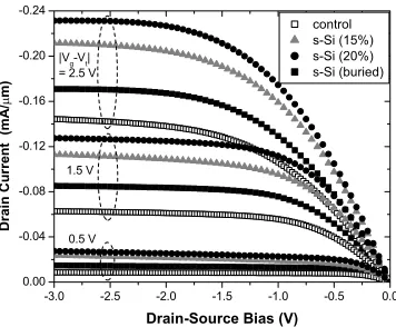
Fig. 1. The drain-current as a function of source-drain voltage for gate overdrive voltages of 0.5, 1.5 and 2.5 V. All devices have a lithographic gate length of 0.3µm and 5µm width and all measurements are dc.
then grown followed by the channel layers. The thickness of this spacer layer was chosen after modelling the As diffusion during the high thermal budget fabrication process to produce a retrograde doping profile for the n-type wells. N-type dopant diffusion of As and P in SiGe is known to be larger than that in bulk Si [25] but there is little accurate data in the literature for the diffusivity of n-type dopants in SiGe. Therefore the setback of the dopant was modeled using diffusion data for Si [26]. All process steps with thermal anneals above 400oC were included in the diffusion modeling. Simulations indicate that a 50 nm spacer will result in a channel doping of less than 1016
cm−3
whilst providing good subthreshold characteristics. On the Si0.85Ge0.15virtual substrate a 20 nm i-Si layer was
grown and a 17 nm i-Si on the Si0.8Ge0.2 virtual substrate.
Both these tensile strained-Si layers are below the Matthews and Blakeslee critical thickness [27] and should therefore be stable to high temperature processing [28][29]. The buried channel device was grown on top of a Si0.85Ge0.15 virtual
substrate and consisted of a 50 nm undoped Si0.85Ge0.15
spacer, a 10 nm undoped compressively-strained Si0.7Ge0.3
channel and a 10 nm undoped tensile-strained Si cap. This cap thickness was chosen after a number of simulations to calculate the consumption of the cap through cleans, thermal oxide growth and also Ge diffusion [30] from the Si0.7Ge0.3
channel. At least 2 nm of Si cap should remain after the devices have been processed. This is especially important as any Ge incorporated into the oxide would create defect states or result in Ge pileup at the SiO2 interface increasing the
interface trapped charge density and reducing the transistor performance [31][32].
Device fabrication followed the process flow of a high-thermal budget 0.25 µm CMOS process [14][23]. Si control wafers were also processed after the n-well was implanted using a three stage phosphorus implant of4×1012
cm−2
dose at 400 keV,2×1013
cm−2
dose at 280 keV and2×1012
cm−2
Fig. 2. The subthreshold plots for the Si control, strained-Si on Si0.8Ge0.2
and buried channel devices. All devices have a lithographic gate length of 0.3 µm and 5µm width.
substrates at any stage was undertaken as previous results have demonstrated significantly higher mobilities [14][23] than CMP polished substrates[13][20]. As CMP is likely to produce off-cut surfaces when the growth and relaxation processes are considered [34], non CMP substrates should be expected to produce higher mobilities [35]. A thermal gate oxide was grown at 800 oC followed by an anneal in a N
2 atmosphere.
Source and drain implants using high doped drain (HDD) and low doped drain (LDD) structures with Si3N4 spacers were
activated with a 1020 oC rapid thermal anneal and a full titanium salicide process was used. Oxide thicknesses of 4.5 nm were extracted from C-V characteristics of300×300µm MOS capacitors.
III. ELECTRICALRESULTS
Fig. 1 shows the measured drain current,Ids as a function of source-drain bias Vds for as-drawn 0.3 by 5 µm (Lg by W) devices at three values of gate overdrive|Vg−Vt|where Vg is the gate voltage and Vt is the threshold voltage. On-current enhancements are observed for each of the strained-Si devices including the buried channel over the bulk strained-Si controls. At |Vg−Vt|=−Vds = 2.5 V,Ids for the strained-Si surface channel device on strained-Si0.85Ge0.15 exceeds that of
the control by 50%, whereas for the strained-Si device on Si0.8Ge0.2 the enhancement is 60%. The enhancements are
higher at lower gate overdrive (|Vg−Vt| = 1.5 V) due to the result of reduced self-heating in the strained-Si devices [36] since only dc measurements of devices are presented in this paper. It is apparent from Fig. 1, however, that the current drive performance is considerably lower for the buried channel device than for the surface channel strained-Si devices. Ids enhancements of the buried channel device over the Si control of 38% at -1.5 V and 21% at -2.5 V are observed.
[image:3.612.83.264.54.201.2]The subthresholdIdsversus|Vg−Vt|characteristics for the same strained-Si (20%), buried channel and control devices are plotted in Fig. 2. All the devices exhibit on-current/off-current ratios of at least seven orders of magnitude, suggesting, together with the extracted values of subthreshold slope, S that electrostatic integrity is not seriously compromised in the strained-Si devices. The strained-Si and buried channel devices
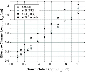
Fig. 3. The effective channel length as extracted by the shift and ratio technique versus the drawn or lithographic gate length for the 4 different wafers.
actually have better subthreshold slopes that the Si control devices.
IV. EFFECTIVECHANNELLENGTH
The plotting of performance parameters as functions of lithographic gate length, Lg, however, can be misleading especially for submicron LDD MOSFETs. In such cases, the effective channel length Lef f is normally taken as the independent variable rather than Lg in comparing channel-length dependent performance parameters [37]. Particularly in LDD structures, the lateral straggle in the source and drain doping can actually causeLef f to increase significantly with respect to Lg, as can a retrograde, setback or modulation doping profile [37]. Furthermore,Lef f may exhibit a strong dependence on gate bias at low gate overdrives |Vg−Vt|
because of the virtual channel which forms in the LDD regions under or close to the gate contact [38]. The diffusivities of dopants in strained-Si and SiGe are expected to be higher than in bulk Si especially for the p-type implant boron used for the Ohmic contacts [39], possibly leading to different LDD and HDD source and drain profiles and hence different metallurgical as well as effective channel lengths. Lef f is effectively a measure of the length over which a gate bias can invert charge in the substrate to form a channel, and is also found to be sensitive to the doping profile perpendicular to the channel; it is found to be significantly longer than the metallurgical gate length in the case of retrograde doping [37] and for buried channel Si pMOSFETs [40]. In fig. 3Lg is plotted against Lef f for the Si controls and the surface-and buried-channel strained-Si devices. The shift surface-and ratio method forLef f extraction was used and is described in detail elsewhere [23][37]. For the shortest channel length devices, Lg is longer than Lef f for the strained-Si surface channel devices, as expected from enhanced source and drain diffusion, compared with the controls. For the buried channel devices, Lef f is indeed significantly higher by approximately 0.2µm, as anticipated.
p-Fig. 4. The drain-current as a function of source-drain voltage for gate overdrive voltages of 0.5, 1.5 and 2.5 V. All the devices have an effective channel length of 0.25µm and width of 5µm.
MOSFETs and the Si control. For|Vg−Vt|=−Vds= 1.5V, Idsfor the strained-Si surface channel device on a Si0.85Ge0.15
virtual substrate exceeds that of the control by 45%, for the strained-Si device on the Si0.8Ge0.2 virtual substrate the
enhancement is 57% and the buried channel has a 92% en-hancement. These values are reduced for an applied bias of 2.5 V to 24%, 22% and 71% respectively again demonstrating the self-heating in the devices [36]. It must be stated that enhanced performance from the buried channel transistor is a device with a lithographically or as-drawn gate length around 0.2µm smaller than some of the other devices in the same plot and demonstrates one of the disadvantages of the buried channel design in that the gate has less control of the channel since it is further from the gate. The results also demonstrate that the band-offset of the heterostructure also plays a significant rˆole in changing the effective channel length of a device. As the cost of lithographically typically increases exponentially with the exponential decrease in minimum feature size [3][8], this is a significant disadvantage for the buried channel device.
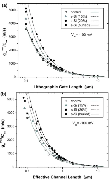
The maximum transconductance, gmax
m per unit width di-vided by the oxide capacitance, Cox versus lithographic and effective channel lengths are plotted in Fig. 5(a) and 5(b) respectively. Thegmax
m /Cox is a measure of the hole velocity and therefore is a good measure of material performance which should be relatively device independent. It is also independent of oxide thickness allowing the values to be easily compared to other devices with substantially different oxide thicknesses. Again the performance of the buried channel device is above that of the control Si sample for the lithographic gate lengths but below the strained-Si surface channel devices. When the effective channel length is plotted, the buried channel device is superior to all the other devices for all gate lengths (Fig. 5(b)). Enhancements over the Si control of 23% for the strained-Si on Si0.85Ge0.15 virtual substrates, 45% for the strained-Si on
Si0.8Ge0.2 virtual substrates and 62% for the buried channel
devices were measured for an effective channel length of 0.25 µm for a low source-drain bias of -0.1 V.
Fig. 6 shows the drain induced barrier lowering (DIBL) as a function of lithographic gate length. No significant increase in the roll-off is observed for the strained-Si devices, indicating that electrostatic integrity is conserved notwithstanding the
[image:4.612.347.528.49.344.2](b)
Fig. 5. (a) The velocity of the holes (that isgmax
m /Cox) versus the drawn
or lithographic gate length for the four wafers for device widths of 5µm. (b) The velocity of the holes (that isgmax
m /Cox) versus the effective channel
length.
strain, in spite of the high thermal budgets employed in the fabrication of the devices. The buried channel devices have almost comparable performance to the control Si device down to 0.2µm drawn gate length.
A. Effective Mobility
Effective mobilities µef f as functions of vertical effective electric fieldsEEf f were calculated for long channel devices (L= 100µm) according to the expressions
µef f = L
Wgd(Vg)Qinv (1)
and
Eef f = 1
Si(Qb+ηQinv) (2)
whereη = 1/3 for holes andQinv and Qb are the inversion layer (i.e. channel) and the bulk (depletion) charge densities, respectively. The drain conductancegd(Vg)was obtained from
−Id(Vg)/Vdsmeasured at low drain bias (Vds= 10mV). The charge densities are computed from split C-V measurements [41][42]:
Qinv=
Z ∞
Vg
CgcdVg (3)
[image:4.612.86.266.54.198.2]µ
Fig. 6. The drain induced barrier lowering (DIBL) as a function of effective channel length for 5µm wide devices.
Qb=
Z Vf b
Vg
CgbdVg (4)
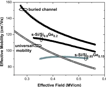
where Cgc is the gate-to-channel and Cgb the gate-to-body capacitance (per unit area). The flat-band voltage Vf b which limits the integration in (4) is determined from the high-frequency MOS-C capacitance measurements [43], and the overlap capacitance was subtracted fromCgc before perform-ing the integration in (3). Theµef f−Eef f characteristics for the buried and strained-Si devices are plotted in Fig. 7 along with the universal mobility curve for a bulk Si p-MOS device. The control sample had effective mobility below the universal curve and has been omitted for clarity. The results for the strained-Si devices on both the Si0.85Ge0.15and the Si0.8Ge0.2
virtual substrates show modest enhancements compared to the universal curve and are comparable to many results in the literature [13][15]. Both of these mobilities are significantly below the values calculated by the theory of Oberhuber et al. [44] for strained-Si p-MOS devices at these Ge contents. The buried channel device does demonstrate significantly higher mobility of a 40% enhancement over the universal curve at an effective electric field of 0.55 MV/cm. While the theory of Oberhuber et al. [44] is only for strained-Si surface channel devices, the value of 40% enhancement for the buried channel is much closer to the value predicted by the theory for surface channel devices.
V. CONCLUSION
Enhanced performance over bulk Si and strained-Si p-MOS devices fabricated on Si0.85Ge0.15 and Si0.8Ge0.2
vir-tual substrates has been demonstrated from a compressively strained, buried quantum well Si0.7Ge0.3channel p-MOSFET.
For |Vg−Vt| = −Vds = 1.5 V, Ids the strained-Si surface channel device on a Si0.85Ge0.15 virtual substrate exceeds
that of the control by 45%, for the strained-Si device on the Si0.8Ge0.2 virtual substrate the enhancement is 57% and
the buried channel has a 92% enhancement. The extracted effective mobility from long-channel transistors for the buried channel device is over 40% greater than the universal mobility curve for bulk Si p-MOS devices at 0.55 MV/cm vertical effective electric fields. Enhancement in the hole velocity were
s-Si/Si0.8Ge0.2 buried channel
s-Si/Si0.85Ge0.15 universal
mobility
Fig. 7. The effective mobility as a function of the vertical electric field for the strained-Si and buried channel devices with the universal mobility of bulk Si control devices plotted for comparison.
also demonstrated over the Si control of 23% for the strained-Si on strained-Si0.85Ge0.15 virtual substrates, 45% for the strained-Si
on Si0.8Ge0.2virtual substrates and 62% for the buried channel
devices were measured for an effective channel length of 0.25 µm for a low source-drain bias of -0.1 V. The enhancement over the strained-Si p-MOS devices is only evident when devices with the same effective channel length are compared and this is reversed when constant lithographic or as-drawn gate lengths are compared. The effective channel length was around 0.2µm longer than the as-drawn or lithographic gate length for all gate lengths below 1µm which may preclude the use of such buried technology devices as significantly shorter gate-length devices are required to be fabricated to obtain performance enhancements over strained-Si technology.
REFERENCES
[1] B. S. Meyerson, ”Silicon:germanium-based mixed-signal technology for optimization of wired and wireless telecommunications”, IBM J. Res. Dev., vol. 44, no. 3, pp. 391-407, 2000.
[2] S. C. Jain, S. Decoutere, M. Willander and H. E. Maes, ”SiGe HBTs for applications in BiCMOS technology: I. Stability, reliability and material parameters,” Semicond. Sci. Technol., vol. 16, pp. R51-R65, 2001. [3] 2003 International Technology Roadmap for Semiconductors. [Online].
Available: http://public.itrs.net.
[4] M. V. Fischetti, ”Long-range Coulomb interactions in small Si devices. Part II. Effective electron mobility in thin-oxide structures,” J. Appl. Phys., vol. 89, no. 2, pp. 1232-1250, 2001.
[5] M. Dragosavac, D. J. Paul, M. Pepper, A. B. Fowler and D. A. Buchanan ”Electron effective mass in ultra-thin gate-oxide silicon MOSFET inver-sion layers” Phys. Rev. Lett. (Submitted for publication).
[6] J. Welser, J. L. Hoyt, S. Takagi and J. F. Gibbons, ”Strain dependence of the performance enhancement in strained-Si n-MOSFETs,” in IEDM Tech. Dig., 1994, pp. 373-376.
[7] A. G. O’Neill and D. A. Antoniadis, ”Deep submicron CMOS based on silicon germanium technology,” IEEE Trans. Electron Devices, vol. 43, no. 6, pp. 911-918, 1996.
[8] D. J. Paul, ”Silicon-germanium strained layer materials in microelectron-ics,” Adv. Mater., vol. 11, no. 3, pp. 191-204, 1999.
[9] M. M. Rieger and P. Vogl, ”Electronic-band parameters in strained Si1
−xGex alloys on Si1
−yGey substrates” Phys. Rev. B, vol. 48, no.
19, pp. 14276-14287, 1993.
[10] M. V. Fischetti and S. E. Laux, ”Band structure, deformation potentials and carrier mobility in strained Si, Ge, and SiGe alloys,” J. Appl. Phys., vol. 80, no. 4, pp. 2234-2252, 1996.
[11] K. Rim, J. L. Hoyt and J. F. Gibbons, ”Fabrication and analysis of deep submicron strained-Si n-MOSFETs,” IEEE Trans. Electron Devices, vol. 47, no. 7, pp. 1406-1415, 2000.
[image:5.612.349.526.52.198.2]performance of SiGe/Si MOSFETs,” Solid-State Electron., vol. 46, pp. 1925-1932, 2002.
[19] T. Mizuno, N. Sugiyama, A. Kurobe and S. Takagi, ”Advanced SOI p-MOSFETs with strained-Si channel on SiGe-on-insulator substrate fabricated by SIMOX technology,” IEEE Trans. Electron Devices, vol. 48, no. 8, pp. 1612-1618, 2001.
[20] C. W. Leitz et al., ”Hole mobility enhancements in strained Si/Si1−yGey
p-type metal-oxide-semiconductor field-effect transistors grown on re-laxed Si1−xGex (x<y) virtual substrates,” Appl. Phys. Lett., vol. 79,
no. 25, pp. 4246-4248, 2001.
[21] G. H ¨ock, E. Kohn, C. Rosenblad, H. von K¨anel, H.-J. Herzog and U. K ¨onig, ”High hole mobility in Si0.17Ge0.83 channel
metal-oxide-semiconductor field-effect transistors grown by plasma-enhanced chemi-cal vapor deposition,” Appl. Phys. Lett., vol. 76, no. 26, pp. 3920-3922, 2000.
[22] H. von K¨anel, M. Kummer, G. Isella, E. Mller and T. Hackbarth, ”Very high hole mobilities in modulation-doped Ge quantum wells grown by low-plasma enhanced chemical vapor deposition,” Appl. Phys. Lett., Vol. 80, no. 16, pp. 2922-2924, 2002.
[23] M.P. Temple, et al., ”Enhanced p-MOSFET performance using strained-Si on strained-SiGe virtual substrates grown by low energy plasma enhanced chemical vapor deposition” IEEE Trans. Elec. Dev.(Submitted for publi-cation).
[24] S.H. Olsen et al., ”Impact of virtual substrate growth on high perfor-mance strained Si/SiGe double quantum well metal-oxide-semiconductor field effect transistors,” J. Appl. Phys., vol. 94, no. 10, pp. 6855-6863, 2003.
[25] J. L. Hoyt, H. M. Nayfeh, S. Eguchi, I. Aberg, G. Xia, T. Drake, E. A. Fitzgerald and D. A. Antoniadis, ”Strained silicon MOSFET technology” in Proc. IEDM 2002, pp. 23-26.
[26] ”Athena 2D process simulation software,” Silvaco International: Santa Clara, CA.
[27] J. W. Matthews and A. E. Blakeslee, ”Defects in epitaxial multilayers,” J. Cryst. Growth, vol. 27, pp. 118-125, 1974.
[28] A.C. Churchill et al., ”Two-dimensional electron gas mobility as a function of virtual substrate quality in strained Si/SiGe heterojunctions,” J. Vac. Sci. Technol. B, vol. 16, no. 3, pp. 1634-1638, 1998.
[29] D. J. Paul, A. Ahmed, A.C. Churchill, D. J. Robbins and W. Y. Leong, ”Low-dimensional inverted Si/SiGe modulation-doped electron gases using selective ex-situ ion implantation,” Mat. Sci. Eng. B, vol. 89, no. 1, pp. 111-115, 2002.
[30] H. Klauk, T. N. Jackson, S. F. Nelson and J. O. Chu, ”Thermal stability of strained and unstrained-Si” Appl. Phys. Lett., vol. 68, no. , pp. 1975-1977, 1996.
[31] J. Eug´ene, F. K. LeGoues, V. P. Kesan, S. S. Iyer and F. M. dHeurle, ”Diffusion versus oxidation rates in silicon-germanium alloys,” Appl. Phys. Lett., vol. 59, no. 1, pp. 78-80, 1991.
[32] F. K. LeGoues, R. Rosenberg, T. Nguyen, F. Himpsel and B. S. Meyer-son, ”Oxidation studies of SiGe,” J. Appl. Phys., vol. 65, no. 4, pp1724-1728, 1989.
[33] A. M. Waite, Y. T. Tang and A. G. R. Evans, unpublished [34] A. J. Pidduck et al., ”On the growth of high quality relaxed Si1
−xGex
layers on Si by vapour phase epitaxy,” in Inst. Phys. Conf. Ser., no. 157, 1997, pp. 135-144.
[35] S. H. Olsen et al., ”Strained Si/SiGe n-channel MOSFETs: Impact of surface cross-hatching on device performance,” Semicond. Sci. Technol., vol. 17, pp. 655-661, 2002.
[36] K. A. Jenkins and K. Rim, ”Measurement of the effect of self-heating in strained-silicon MOSFETs,” IEEE Electron Device Lett., vol. 23, no. 6, pp. 360-362, 2002.
mobility in thin dielectric MOS transistors,” Solid-State Electron., vol. 25, pp. 833-841, 1982.
[43] D. K. Schroder, Semiconductor Material and Device Characterization, 2nd Ed. New York, Wiley, 1998.
[44] R. Oberhuber, G. Zandler and P. Vogl, ”Subband structure and mobility of two-dimensional holes in strained Si/SiGe MOSFET’s” Phys. Rev. B, vol. 58 no. 15, pp. 9941-9948, 1998.
Matthew P. Temple received the B.Eng. degree
in 1996 and the Ph.D. degree in 2001, both in Electronic and Electrical Engineering, from the Uni-versity of Birmingham, U.K., where his research interests were Er-doped Si thin film devices and the simulation of hot carrier tunneling in MOSFETs. In 2001 he joined the Semiconductor Physics Group at the Cavendish Laboratory, University of Cambridge, where he is currently investigating strained-Si/SiGe MOSFETs. Dr. Temple is a member of the Institute of Physics.
Douglas J. Paul (M00) was born in Greenock, U.K.,
Yue T. Tang was born in Sungai Siput, Perak,
Malaysia, in 1973. He received the B.Eng. degree in electronics engineering from the University of Nottingham, Nottingham, U.K., in 1995 and the M.Sc. degree in microelectronics system design and Ph.D. degree from the University of Southampton, Southampton, U.K., in 1997 and 2000, respectively. Since 2000, he has been a Post-doctoral researcher in the Microelectronics group at the University of Southampton. From 2000 to 2001, he worked on modeling and design of heterojunction bipolar tran-sistor on silicided SOI. Since 2001, his research interest involves design, fabrication, modeling and development of heterojunction MOS.
Andrew M. Waite was born in Portsmouth. U.K.,
on February 1, 1971. He received the B.Eng. and Ph.D. degrees from the University of Southampton, Southhampton, U.K. in 1993 and 1999, respectively. His Ph.D. work concentrated on the creation and hot carrier degradation of raised source/drain MOS-FETs. He was a fellow of the European Commission SUSTAIN program between 1995 and 1996, where he worked at IMEC, Leuven, Belgium. He now works as a Research Fellow at the University of Southampton, where his research interests include the integration of strained silicon into CMOS processes, pseudomorphic strained SiGe MOSFETs, and raised source/drain MOSFETs.
Claudia Cerrina was born in Turin, Italy, in 1970.
She graduated in Chemistry from the Universit degli studi di Catania, Catania, Italy, in 1996, becoming a chartered chemist in 1997. In 2003, she received the PhD degree in Electrical and Electronic Engineering from the University of Surrey, Guildford, UK, for her research into dopant activation and carrier transport in ion beam synthesized SiGe. She joined the Micro-electronics Group at the University of Southampton, Southampton, UK, in 2002, where she is working on fabrication and development of heterojunction MOS devices.
Alan G. R. Evans received the B.Sc. degree in
physics from Liverpool University, Liverpool, U.K., in 1966, and the D.Phil. degree from Oxford Univer-sity, Oxford, U.K. in 1969. He has been a University academic since 1969 having worked at the Uni-versities of Sheffield, Strathclyde, and Southamp-ton in the U.K. He has worked on a variety of semiconductors, including InSb, InP, GaAs, SiGe, Si and poly-Si, studying electrical properties, device characteristics and device fabrication technologies. His recent work has been focused on MEMS devices and the use of SiGe in MOS transistors. He is a Professor with the Department of Electronics at Southampton University, Southampton, U.K., and the Joint Head of the Microelectronics Group there. His research interests have been in the area of semiconductor materials, devices and technologies.
PLACE PHOTO HERE
Xiaobing Li biography unavailable
Jing Zhang received the B.Sc. degree in Physics
from Peking University, China in 1978, the B.Sc. degree in Physics from Imperial College, London in 1983 and PhD degree from Imperial College, Lon-don in 1986. After working at the Philips Research Laboratories, Redhill, and being a visiting scholar at Wolfson College, university of Oxford, he returned to the Experimental Solid State Physics Group at Imperial College where he is at present a Senior Lecturer. His research concentrates on the physics of materials with a focus on the epitaxial growth of semiconductor thin films using molecular beam epitaxy (MBE) and gas source MBE.
Anthony G. ONeill received the B.Sc. degree in