This is a repository copy of
Electric field domains in p-Si/SiGe quantum cascade
structures
.
White Rose Research Online URL for this paper:
http://eprints.whiterose.ac.uk/1110/
Article:
Ikonic, Z., Harrison, P. and Kelsall, R.W. (2006) Electric field domains in p-Si/SiGe
quantum cascade structures. IEEE Transactions on Electron Devices, 53 (2). pp. 189-195.
ISSN 0018-9383
https://doi.org/10.1109/TED.2005.862498
[email protected] https://eprints.whiterose.ac.uk/ Reuse
See Attached
Takedown
If you consider content in White Rose Research Online to be in breach of UK law, please notify us by
Electric Field Domains in p-Si/SiGe
Quantum Cascade Structures
Zoran Ikonic´, Paul Harrison
, Senior Member, IEEE
, and Robert W. Kelsall
Abstract—The formation of domains in quantum cascade struc-tures is one of the mechanisms strongly affecting the operation of quantum cascade lasers, quantum-well infrared detectors, and other devices. In this paper, we consider the problem of domain formation in p-doped Si/SiGe quantum cascades, using a carrier scattering transport framework. In effect, the hole flow along the cascade is described via scattering between quantized states be-longing to neighboring periods, caused by phonons, alloy disorder, and carrier–carrier interactions. The generation of either periodic or of nonperiodic domains is studied in uniformly doped cascades, as well as the influence of modulation doping of cascades on the domain formation.
Index Terms—Domain formation, quantum cascade structures, SiGe.
I. INTRODUCTION
B
IASED semiconductor quantum-well cascade structures, as are used nowadays in intersubband infrared photode-tectors [1], [2], lasers [3], and Bloch oscillator type devices [4], [5] are well known to be susceptible to the formation of elec-tric field domains. The homogeneous elecelec-tric field in a struc-ture is broken, due to charge redistribution over individual wells and the appearance of the associated space-charge contribution to the potential. The effect is related to the existence of nega-tive differential resistivity (NDR) of the heterostructure, and is detrimental for the normal operation of devices. The problem of domain formation has been addressed in a number of papers [2], [6]–[17], and methods of avoiding it have also been consid-ered recently [18]. The NDR is usually ascribed to resonant tun-neling between quantized states in neighboring wells. However, current thought puts scattering, rather than resonant tunneling, as the dominant mechanism of carrier transport in quantum cas-cade lasers [19]. This can nethertheless bring about NDR, be-cause various scattering mechanisms depend strongly on rela-tive alignment of relevant states (depending on the scattering mechanism), and a suitable bias can considerably enhance the total scattering rate, and hence the current. Such current peaks are much broader than those predicted by resonant tunneling. In this work we consider the formation of stationary periodic do-mains in p-type Si/SiGe quantum cascade structures.Manuscript received April 11, 2005; revised August 26, 2005. This work was supported in part by Defense Advanced Research Projects Agency/U.S. Air Force under Contract F19628-99-C-0074, and EPSRC, U.K., under Grant GR/S27528/01. The review of this paper was arranged by Editor S. Datta.
The authors are with the Institute of Microwaves and Photonics, School of Electronic and Electrical Engineering, University of Leeds, Leeds LS2 9JT, U.K.
Digital Object Identifier 10.1109/TED.2005.862498
II. THEORETICALCONSIDERATIONS
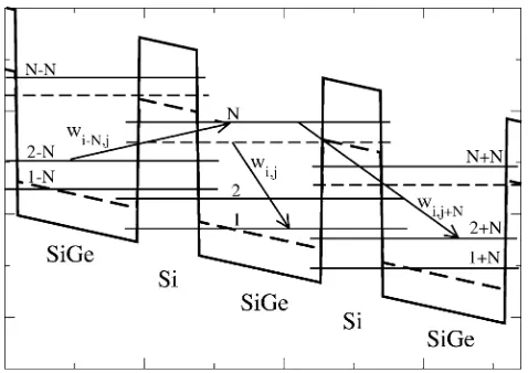
Hole transport is described via “upstream” and “downstream” scattering between quantized subbands in neighboring wells, which are calculated using the 6 6 method including the full anisotropy of the heavy hole and light hole subbands. The scattering mechanisms taken into account are deformation potential (acoustic and optical phonons), alloy disorder, and car-rier-carrier scattering. Various details of the hole transport cal-culation in uniformly biased cascade structures have been de-scribed previously [20], [21], and here we give a brief outline. All the subbands found in a cascade are grouped into sets which “belong,” i.e., are formally assigned to its individual periods. This is based on the wavefunction localization properties: if a larger fraction of a wavefunction is in a particular period than in any other, then the state is assigned to that particular period. This certainly does not imply that a state is fully localized in the period it is assigned to: The wavefunctions are frequently spread to some extent over a few neighboring periods, and this overlap with neighboring states is of crucial importance for the existence of scattering transport. The formal assignment is im-portant in order to avoid overcounting or leaving out some of the states that exist in a long cascade. More technical details on how this assignment is performed for hole states are given in [20]. The states in a uniformly biased cascade have the translation invariance property, i.e., by a spatial shift of the wavefunction by one period and an energy shift by the potential drop per pe-riod, one gets another real state of the cascade. This property en-ables one to (re)construct all the states in a cascade, starting with those assigned to one period and performing the above replica-tion procedure. By the same token, all periods of a uniformly biased cascade have identical carrier distributions, so it suffices to consider explicitly just one period and its interaction with the (nearest) neighbors, and therefore to handle a small number of states, rather than all the states of a long cascade simultane-ously. In order to find the current and carrier distribution over states in a uniformly biased cascade, one solves the system of rate equations describing the in- and out-scattering of holes from the states involved, Fig. 1. These in turn require the scattering rates between all states, either assigned to the same period or to neighboring periods. While only the latter type of scattering di-rectly contributes to the current, the intraperiod scattering takes part in establishing the hole distribution over the available states, and thus also affects the current indirectly. The dependence on scattering rates on both the lattice and carrier temperatures, as well as on subband populations, are included. The carrier tem-peratures in each subband are calculated using the energy bal-ance approach [21], i.e., by solving simultaneously the particle number and energy balance rate equations. The only assumption
190 IEEE TRANSACTIONS ON ELECTRON DEVICES, VOL. 53, NO. 2, FEBRUARY 2006
Fig. 1. Scattering transport model of the quantum cascade structure.
made in this method is that the hole distributions within indi-vidual subbands are Fermi–Dirac like, with their indiindi-vidual tem-peratures and Fermi levels; our Monte Carlo simulations [20] indicate that this is a reasonable approximation for calculating the current–voltage dependence.
In order to explore domain formation the system of rate equa-tions, as given in [21], has been modified here to account for inhomogeneous electric fields in the cascade. The scattering co-efficients between different pairs of states each depend differ-ently on the bias field [7]. Here, we make the approximation of discretizing the Poisson equation, using only the values at the central points of the wells. The electric field is then piece-wise-linear. The scattering coefficients between two states longing to neighboring wells depend on the electric field be-tween these wells. On the other hand, the coefficients bebe-tween states in the same well depend on the field inside it, but since this is not defined within the discretized-Poisson model we use the average of the fields to the left and to the right (it should be noted, though, that this dependence is quite weak, in contrast to the case of interwell scattering coefficients). Taking the set of states per period, so that labels states within a
particular ( th) period, and labels
states in its right or left neighbors, the rate equations read
(1)
where the subscripts , and run over all states of the pe-riod, while denotes the particular well ( and denote the
electric fields to the right or to the left), is the 2-D density of holes in quantized state of the th well, is the transi-tion rate from state into state due to all single-hole scattering rates, and are the transition rates due to carrier-carrier scattering. Note that only two of the latter type of processes are given explicitly in (1), others may be written in the form analogous to the single-hole scattering terms. As dis-cussed previously [21], due to the translational invariance in a homogeneous cascade it is sufficient to calculate the scattering coefficients within a well and toward its right-hand neighbor, and substitute, e.g., by in (1), but the field at which this is taken (denoted as “ ”) remains unchanged.
The discretized Poisson equation reads [7]–[13]
(2)
where is the two-dimensional (2-D) acceptor doping density in the th well, the dielectric permittivity, and the struc-tural (growth) period, which we hereafter call the unit cell. In writing (2) the distributed nature of the space charge, which arises from extension of the wavefunctions over several het-erostructure layers, is ignored. This widely used approxima-tion holds well for holes, which generally have more strongly localized wavefunctions than electrons, and is consistent with the way in which the wavefunctions are used in the calculation. A fully self-consistent solution with the delocalized wavefunc-tions and the interwell potential would be prohibitive here, be-cause for holes the wavefunction localization is strongly depen-dent on in-plane wave vector [20].
distributions in the contact well were investigated: 1) carrier distributions set equal to those in the immediately adjacent wells, and 2) carriers assumed to occupy only the ground subband of the contact wells. In both cases, the bias-dependent scattering rates used inside the cascade were also employed for calculating the scattering into or out of the contacts.
Numerical simulations of domain formation in a cascade structure conducted in [7] involved finding the steady-state solution to the system of time-dependent rate equations upon increasing the bias in small increments, and the initial state of the system was taken as the steady state at the previous bias point. The picture of domain formation and evolution was consistent with earlier views gained by physical insight, e.g., [2]. These show that a cascade has one low-field and one high-field region, and the increasing bias expands the high-field portion at the expense of the low-field one, as one by one each well switches from the low-field into the high-field state. More recently there have been detailed studies [12]–[16], reporting that a homogeneous carrier and field distribution in an n-type multiple quantum-well photodetector evolves into a period-doubled configuration, so as to form space-charge (and field) domains that are periodic and include two structural periods of the cascade. These results, which appear at odds with the low/high field domain picture, were also obtained by evolving the system in time, but under somewhat different conditions than in [7]: the carrier density was increased (by illumination) abruptly in the region where domain formation became possible. Periodic domains may generally include any number of unit cells, although only the two-cell periods have actually been found by numerical simulations [12]–[16].
The approach we use in this work to investigate the domain formation relies on solving the system of nonlinear equations, (1) and (2), in the steady state. This is computationally more demanding than tracking the time evolution of the system, but enables one to find all the solutions and avoid getting trapped in the first stationary point that the evolving system encounters. The price to pay is that the size of the system which can be handled is limited: for more than 12 or so periods it becomes difficult to find solutions that are remote from the starting point, which effectively precludes the “finding all solutions” feature. Certainly, both periodic and nonperiodic domains can be inves-tigated by this approach.
We consider the periodic case first, and let denote the number of unit cells per period. The periodicity implies that and in (1), and similar translations apply for the scattering coefficients. In the steady-state , then, out of the total of algebraic (1) one is linearly depen-dent on the others, and is replaced by the particle conservation
law: . There are also equations of type
(2), which completes the full system. If the carrier temperatures, and hence the scattering rates, are known, these may be solved for unknowns. Since the system is nonlinear, it will have more than a single solution. Depending on the parameters (values of the scattering coefficients, bias and doping) all except one of them may be unphysical (i.e., give negative values for one or more densities), while the only physically acceptable solu-tion is the homogeneous one, with each well having an identical distribution of holes over its quantized states, and with all the
space-charge-induced contributions to the potentials equal to zero. Alternatively, more than one physical solution may some-times be found, and this denotes domain formation. It is inter-esting to note that the charge neutrality (within one period) im-plicitly appears in the model via the particle conservation law given above. It is not possible to equate the total density of free carriers to anything else but the total doping , because the excess charge would then induce global bowing of the poten-tial; the domain periods would cease to be identical; hence the periodic model would fail.
The situation is different for the nonperiodic case. With a set of fixed boundary conditions all equations in the system (1) are independent. Moreover, the system (1)–(2) is complete, so in fact there is no place in it for a constraint which would be equiv-alent to the charge neutrality: whether or not neutrality occurs can only arise from the calculation. In a real device, any de-parture from charge neutrality within the heterostructure itself would be balanced by the formation of a space charge region within the semiconductor contact layer, which is not included in our model.
In actual calculations the scattering coefficients are tabulated at a number of electric field and hole density values, and these are then used, via interpolation, to solve the system (1)-(2). This is because the evaluation of scattering coefficients is com-putationally very demanding, and root-finding routines require many function calls, which makes it impossible to execute the full self-consistent energy balance calculation as many times as is needed by the root-finding procedure. Technically, dif-ferent solutions are found by running the root-finder many times – with a randomly generated starting point in each run. For each solution found, we note that with the solution(s) found, the current density is evaluated by accounting for all car-riers which pass through some reference plane; e.g., the inter-face between a particular ( th) period and the adjacent, th period [21].
An approximate “macroscopic” model of domain formation may be constructed by considering only the field dependence of the current density , for each period. The latter should be calculated for different values of carrier density, and it is implic-itly assumed that the carrier distribution over quantized states remains the same as in the homogeneous cascade; it is only the total carrier density in a well that may vary. This approach greatly reduces the number of equations. In the period-doubling case, for instance, there are just two equations (one of which is linear), regardless of the actual number of states in a well
(3)
where is the excess hole charge density in a particular well, and is its forward field. A comparison between this approx-imate model and our full, microscopic scattering model is given in the following section.
III. NUMERICALRESULTS ANDDISCUSSION
192 IEEE TRANSACTIONS ON ELECTRON DEVICES, VOL. 53, NO. 2, FEBRUARY 2006
Fig. 2. Current densityJversus bias fieldFcalculated for the homogeneous cascade described in the text, for different values of doping density per period.
and 8 monolayer (2.15 nm) wide Si barriers, grown on a Ge Si virtual substrate. It has just two low-lying subbands per period, the ground HH1 and the first excited, LH1 subband; the next, HH2 subband may be ignored because it is much higher in energy and almost empty. The LH1-HH1 energy spacing of 28 meV is primarily determined by the strain in the quantum-well layers. At a field of 42 kV/cm the HH1 subband from the preceding (higher) well and the LH1 subband of the next (lower) well at are aligned. However, for finite the alignment appears at different fields, because of the different dispersions of the HH and LH subbands, so the phe-nomenon of resonance is not so strong as in the case of n-type heterostructures. As the bias field varies, the spacing between the LH1 and HH1 subbands of the same well changes only slightly, and most of the potential drop per period manifests itself in the displacement of the sets of subbands belonging to adjacent periods.
The calculated current-voltage characteristics for this struc-ture, assuming a homogeneous field, is shown in Fig. 2 for dif-ferent values of doping (i.e., hole) density per period. The cur-rent depends nonlinearly on the density (and this dependence varies with the bias), because it is partly due to hole-hole scat-tering which does not scale linearly with the carrier density. The NDR occurs between 60 and 70 kV/cm, away from where one would expect it, based on the simple considerations of align-ment at and resonant tunneling, and is more prominent at higher carrier densities.
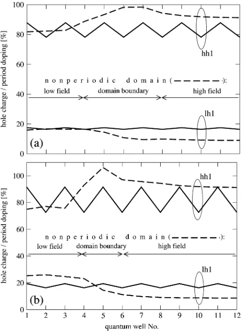
Nonperiodic domains (one high and one low field portion of the cascade) were found at the doping level of approximately cm , with slight variations depending on the type of contact boundary conditions used. In Fig. 3 we plot the population of the two subbands around the domain boundary, which separates the low- and high-field regions. It is interesting to note that this boundary is not very sharp, but actually ex-tends over a region covering a few structural periods. This tran-sition region becomes narrower as the doping increases from its threshold value, as can be seen by comparing Fig. 3(a) and (b). The population of the upper subband, from which the holes scatter more easily into the subsequent period, is consider-ably smaller in the high-field region. The opposite applies to the
Fig. 3. Charge density in the hh1 and lh1 subbands of quantum-wells around the domain boundary in the nonperiodic case (dashed), and in the period-doubled cascade (solid line), with the doping density of
(a)P = 2:5 2 10 cm , and (b)3:5 2 10 cm per period.
ground subband, although the relative modulation depth is smaller. The configurations in which the domains formed did not have strict charge neutrality, but did not deviate much from it, either: the charge accumulation at the domain boundary was partly compensated by a slight depletion elsewhere.
We then searched for periodic domains, as described above, allowing for a domain periodicity of two or more (up to eight). For a homogeneously doped cascade, only domains with a pe-riod of two unit cells were found: imposing a pepe-riodicity of, for example six, produced only three identical two-cell domains, and the homogeneous solution; on the other hand, imposing a periodicity that includes an odd number of unit cells delivers only the homogeneous solution. The two-cell domains occurred at approximately the same density as the contact-related do-mains, at cm , as shown in Fig. 4. This is not surprising, since either type of domain may be viewed as orig-inating from the modulational instability of the homogeneous solution. It is interesting to notice in Fig. 3, where the popula-tion of the two subbands in the periodic case is also shown, that the variation of subband population for the two types of domain is quite different: For periodic domains, it is the ground sub-band population which is more strongly modulated than that of the upper subband.
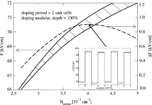
[image:5.594.43.288.64.239.2]Fig. 4. Range of parameters of a homogeneous cascade where domain formation of the period-doubling type occurs (crosshatched area). The size of the electric field redistributed over the two unit cells within the domain period is also shown (dashed line). The prediction of the simple model (3) is shown by the dotted line.
of finite extent; can periodic domains arise if periodicity is not explicitly imposed; and can both types coexist in a sufficiently long cascade? It is not possible to give definite answers, because of limitations upon the length of the cascade we can realisti-cally consider by the present method. In the simulations we per-formed without the assumption of periodicity, we did find pe-riodic domains if the upper subband in the contact wells was populated. On the other hand, if the contacts had only the ground subband populated we never find a periodic do-main structure inside the cascades of limited length considered here. In this respect the existence of periodic domains in a finite length structure appears to be more sensitive to the properties of contacts than is the case for the nonperiodic domains.
There is a simple approximate criterion for the critical doping density (per period) necessary for the formation of stationary depletion type domains [6]
(4)
where and are the field and current
den-sity corresponding to the peak and valley of the NDR part of the dependence. Although is not linearly dependent on , as (4) assumes, the ratio is reasonably constant, and one may estimate that domain formation would require cm . There is a similar criterion for accu-mulation type domains ( is replaced by in the numer-ator of (4)), and this gives a similar value for the critical density, because is not too different from in the cascade con-sidered (see Fig. 2).
[image:6.594.39.290.65.243.2]The agreement of the above criterion with the critical car-rier density that we found necessary for domain formation is very good (in contrast to the simplified model (3) which makes a considerable error in its prediction (see Fig. 4). Indeed, a better agreement could hardly be expected, because the model we use does not assume the equilibrium form of the carrier distribution over subbands in a period—the actual distribution is in fact quite remote from equilibrium, with quite different values of carrier temperatures [21]. The fact that only the 2-cell domains were
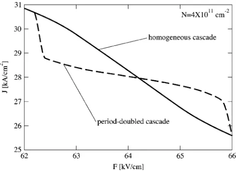
Fig. 5. Current density versus field dependence in the homogeneous configuration and in the case of two-cell periodic domains.
found as stationary solutions agrees with the results obtained previously [12]–[16] by tracking the time evolution of an ini-tially homogeneous electron distribution in multiple quantum-well based photodetectors, with a quite different model from the one used here. It appears thatin realistic cascadesthe two-cell domain structure is not just the solution which is most easily found by the simulation, but is the only possible stationary pe-riodicconfiguration (except the homogeneous one) that may exist under appropriate conditions. This is a consequence of the screening of the local perturbation in space charge, provided by the dielectric response of the semiconductor layers. Indeed, if the permittivity in (2) is artificially reduced to (to be precise, below 2.3 in the example considered) we find that (1) and (2) de-liver more complex domain structures than just the uniform and period-doubled cases. The reduced permittivity, and hence re-duced screening, means that the influence of the space charge perturbation extends over greater distances. Under such condi-tions we do find domain structures comprising three unit cells, with the structure or , or four unit cells with the
structure or , etc.
[where denotes cells with low field, with high field, and n de-notes cells with approximately unchanged, external bias field]. Finally, it is worth noting that the two-cell domains may show long-range modulation instability, which could lead to oscilla-tory or chaotic behavior [13]–[16], but these aspects of domain behavior will not be considered here.
194 IEEE TRANSACTIONS ON ELECTRON DEVICES, VOL. 53, NO. 2, FEBRUARY 2006
Fig. 6. Range of parameters of the modulation doped cascade (doping periodicity equal to 2, modulation depth 20%) for which periodic domains occur.
Fig. 7. Same as in Fig. 6, but for a modulation depth of 100%, for which period doubling occurs (only the upper branchis shown). The average perturbation of the electric field in the period 4 domains, with respect to the “homogenous,” period 2 case, is also shown by the dashed line. The inset shows the well-to-well electric fields in the (dashed) period 2 and (solid) period 4 cases, at doping where their relative deviation is the largest.
modulation doping with a periodicity of two wells, we impose a domain periodicity of four wells. We find two branches of parameters for which domain formation may occur, as shown in Fig. 6 for the case of a doping modulation depth of 20%, meaning that alternate wells are doped to 80% and 120% of the average value. In the rest of the parameter space only the “homo-geneous” solution is found, but it should be noted that the field and charge density in such a solution also alternate in every other quantum-well, due to the periodic variation of doping density.
Whilst increasing the modulation depth reduces slightly the range of parameters for which domain formation occurs (Fig. 7), such domains also become milder, with a much smaller differ-ence between the electric fields in the initial and period-dou-bled field configurations than is the case with homogeneous doping (Fig. 2). The same conclusion applies when increasing the period of modulation doping. In this respect, the modula-tion-doped structures may be considered to be less sensitive to
domain formation, at the expense of having a space-charge elec-tric field already built-in, see the inset in Fig. 7. If the cascade is designed to have such a large difference between the high and low field portions acceptable for its operation (i.e., every other well is “sacrificial”), then it hardly makes any difference whether domain formation has occured or not.
IV. CONCLUSION
The problem of domain formation in p-doped Si/SiGe quantum cascades was considered within the carrier scattering transport framework. Hole transport along the cascade is de-scribed via scattering between quantized states belonging to neighboring periods, caused by phonons, alloy disorder, and carrier-carrier interactions. The influence of modulation doping of cascades on the formation and properties of domains was also studied. The model predicts the formation of both periodic and nonperiodic domains, although the latter only occured with a periodicity of two quantum-wells, and then only under par-ticular contact boundary conditions. We found that increasing the modulation depth does not prevent the domain formation, but makes it progressively more irrelevant whether domain formation has occured or not. This is an important point in the design of p-Si/SiGe quantum cascade laser structures, in which the number of wells per period is preferably low, and doping is required to provide a sufficient carrier density for emission.
REFERENCES
[1] J. L. Pan and C. G. Fonstad, “Theory, fabrication and characterization of quantum-well infrared photodetectors,”Mater. Sci. Eng. R-Rep., vol. 28, pp. 65–147, 2000.
[2] B. F. Levine, “Quantum-well infrared photodetectors,”J. Appl. Phys., vol. 74, pp. R1–R81, 1993.
[3] C. Gmachl, F. Capasso, D. L. Sivco, and A. Y. Cho, “Recent progress in quantum cascade lasers and applications,”Rep. Prog. Phys., vol. 64, pp. 1533–1601, 2001.
[4] P. G. Savvidis, B. Kolasa, G. Lee, and S. J. Allen, “Resonant crossover of terahertz loss to the gain of a Bloch oscillating InAs/AlSb superlattice,”
Phys. Rev. Lett., vol. 92, no. 1–4, p. 196 802, 2004.
[5] H. Kroemer. Large-Amplitude oscillation dynamics and domain sup-pression in a superlattice bloch oscillator. [Online]. Available: [Online] Available: http://www.arXiv.org/cond-mat/0 009 311
[6] A. Wacker, “Vertical transport and domain formation,” inTheory of Transport Properties of Semiconductor Nanostructures, E. Schöll, Ed. London, U.K.: Chapman and Hall, 1998.
[7] F. Prengel, A. Wacker, and E. Schöll, “Simple model for multistability and domain formation in semiconductor superlattices,”Phys. Rev. B, Condens. Matter, vol. 50, pp. 1705–1712, 1994.
[8] A. Wacker, “Semiconductor superlattices: A model system for nonlinear transport,”Phys. Rep., vol. 357, pp. 1–111, 2002.
[9] L. L. Bonilla and H. T. Grahn, “Non-linear dynamics of semiconductor superlattices,”Rep. Prog. Phys., vol. 68, pp. 577–684, 2005.
[10] A. Amann, A. Wacker, L. L. Bonilla, and E. Schöll, “Dynamic scenarios of multistable switching in semiconductor superlattices,”Phys. Rev. E, Stat. Phys. Plasmas Fluids Relat. Interdiscip. Top., vol. 63, no. 1–8, p. 066 207, 2001.
[11] R. Aguado, G. Platero, M. Moscoso, and L. L. Bonilla, “Micro-scopic model for sequential tunneling in semiconductor mul-tiple quantum-wells,” Phys. Rev. B, Condens. Matter, vol. 55, pp. 16 053–16 056, 1997.
[12] M. Ryzhii, V. Ryzhii, R. Suris, and C. Hamaguchi, “Periodic electric field domains in optically excited multiple-quantum-well structures,”
Phys. Rev. B, Condens. Matter, vol. 61, pp. 2742–2748, 2000. [13] V. Ryzhii, I. Khmyrova, M. Ryzhii, R. Suris, and C. Hamaguchi,
[image:7.594.41.289.303.475.2][14] V. Ryzhii and M. Ryzhii, “Nonlinear dynamics of recharging processes in multiple quantum-well structures excited by infrared radiation,”Phys. Rev. B, Condens. Matter, vol. 62, pp. 10 292–10296, 2000.
[15] M. Ryzhii and V. Ryzhii, “Monte Carlo modeling of transient recharging processes in quantum-well infrared photodetectors,”IEEE Trans. Elec-tron Devices, vol. 47, no. 11, pp. 1935–1942, Nov. 2000.
[16] M. Ryzhii, V. Ryzhii, R. Suris, and C. Hamaguchi, “Self-organization in multiple quantum-well infrared photodetectors,” Semicond. Sci. Technol., vol. 16, pp. 202–208, 2001.
[17] L. G. Mourokh, N. J. M. Horing, and A. Y. Smirnov, “Domain forma-tion in a one-dimensional superlattice,”Appl. Phys. Lett., vol. 78, pp. 1412–1414, 2001.
[18] E. S. Daniel, B. K. Gilbert, J. S. Scott, and S. J. Allen, “Simulations of electric field domain suppression in a superlattice oscillator device using a distributed circuit model,”IEEE Trans. Electron Devices, vol. 50, no. 12, pp. 2434–2443, Dec. 2003.
[19] R. C. Iotti and F. Rossi, “Nature of charge transport in quantum-cascade lasers,”Phys. Rev. Lett., vol. 87, no. 1–4, p. 146 603, 2001.
[20] Z. Ikonic´, R. W. Kelsall, and P. Harrison, “Monte Carlo simulations of hole dynamics in SiGe/Si THz quantum cascade structures,”Phys. Rev. B, Condens. Matter, vol. 69, no. 1–9, p. 235 308, 2004.
[21] Z. Ikonic´, P. Harrison, and R. W. Kelsall, “Self-consistent energy balance simulations of hole dynamics in SiGe/Si THz quantum cascade struc-tures,”J. Appl. Phys., vol. 96, pp. 6803–6811, 2004.
Zoran Ikonic was born in 1956 in Belgrade, Yugoslavia. He received the B.Sc., M.Sc., and Ph.D. degrees in electrical engineering from the University of Belgrade, Yugoslavia, in 1980, 1984, and 1987, respectively.
Since 1981, he has been with the Faculty of Electrical Engineering, University of Belgrade. Since 1998, he has been a Full Professor. In 1999, he joined the Institute of Microwaves and Photonics, University of Leeds, Leeds, U.K. His research interests include the electronic structure, optical and transport properties of semiconductor nanostructures, and devices based upon them.
Paul Harrison(SM’99) received the B.Sc. degree from the University of Hull, Hull, U.K. and the Ph.D. degree from the University of Newcastle-upon-Tyne, Newcastle-upon-Tyne, U.K., in 1988 and 1991, respectively.
He was a Postdoctoral Research Assistant at the University of Hull until 1995, when he obtained a Fellowship at the University of Leeds, Leeds, U.K. Since joining the Institute of Microwaves and Pho-tonics, University of Leeds, he has been working on ways to adapt his theoretical and computational ex-perience in semiconductor heterostructures to terahertz sources and detectors. He is Head of the School of Electronic and Electrical Engineering, and currently holds a Chair in quantum electronics. He is author of the bookQuantum Wells, Wires and Dots, 2nd Edition (Wiley, 2005).
Robert W. Kelsallwas born in Rotherham, England, in 1964. He received the B.Sc. (Hons.) and Ph.D. degrees from the University of Durham, Durham, U.K., in 1985 and 1989, respectively. His doctoral research involved studies of electronic transport in GaAs quantum-wells.
From 1989 to 1993, he was a Research Assistant at the universities of Durham and Newcastle-upon-Tyne, developing Monte Carlo simulations of silicon and III-V FETs. He joined the University of Leeds, Leeds, U.K., in 1993 where he is currently Senior Lecturer in the Institute of Microwaves and Photonics. His research interests are in advanced technology microwave, optoelectronic, and molecular-electronic devices. He has published over 200 papers in international journals and at na-tional/international conferences, and is Lead Editor of the bookNanoscale Sci-ence and Technology(Wiley, 2005).