This is a repository copy of Subthreshold diode characteristics of InAs/GaAs quantum dot lasers.
White Rose Research Online URL for this paper: http://eprints.whiterose.ac.uk/97410/
Version: Accepted Version
Article:
Spencer, P., Clarke, E., Murray, R. et al. (3 more authors) (2011) Subthreshold diode characteristics of InAs/GaAs quantum dot lasers. Physical review B: Condensed matter and materials physics, 83 (20). 205407. ISSN 1098-0121
https://doi.org/10.1103/PhysRevB.83.205407
[email protected] Reuse
Unless indicated otherwise, fulltext items are protected by copyright with all rights reserved. The copyright exception in section 29 of the Copyright, Designs and Patents Act 1988 allows the making of a single copy solely for the purpose of non-commercial research or private study within the limits of fair dealing. The publisher or other rights-holder may allow further reproduction and re-use of this version - refer to the White Rose Research Online record for this item. Where records identify the publisher as the copyright holder, users can verify any specific terms of use on the publisher’s website.
Takedown
If you consider content in White Rose Research Online to be in breach of UK law, please notify us by
Sub-threshold diode characteristics of InAs/GaAs quantum
dot lasers
P. Spencer, E. Clarke, R. Murray
Physics Department, Imperial College London, Blackett Laboratory, Prince Consort
Road, London SW7 2AZ, U. K.
K. M. Groom, R. R. Alexander, R. A. Hogg
EPSRC National Centre for III-V Technologies, University of Sheffield, Centre for
Nanoscience & Technology, North Campus, Broad Lane, Sheffield S3 7HQ, U. K.
Abstract
The temperature dependence of the carrier dynamics in ensembles of InAs/GaAs
quantum dots (QDs) are of interest, both from a fundamental point of view but also
because of the consequences for the performance of QD-based optoelectronic devices.
While this topic has been studied before using optical techniques, here we approach
the topic by analyzing the current-voltage (IV) characteristic of QD diodes. Using a
current-modulation technique, the transition from “trap-like” to “thermalized” behavior as the temperature is raised from 80 K to room-temperature is observed.
Furthermore, the results suggest that the IV curve is sensitive to the separate escape of
electrons and holes and the intersubband spacing of the electron states and that of the
I. INTRODUCTION
InAs/GaAs quantum dots (QD) have received much attention for their potential use in
next-generation telecoms light sources [1]. QD-based lasers were predicted to have
low, temperature-insensitive threshold currents [2, 3] but this requires large energy
separations between the discrete QD states to suppress thermal effects. At low
temperatures QD devices do indeed exhibit close to ideal characteristics, but by room
temperature their performance is consistent with thermal spreading across available
energy states with critical temperature values not significantly better than quantum
well lasers [4-6]. In this paper we show that using electrical measurements of the
diode behavior of QD lasers operating well below the lasing threshold, we can obtain
valuable additional information on the transfer of carriers across the diode across a
wide temperature range. Our results are consistent with a gradual onset of carrier
thermalization in the QD ensemble with increasing temperature, as expected, but also
show that there is independent escape of holes and electrons in the mid-temperature
range.
II. SAMPLE DETAILS
The devices studied here were processed from a QD laser structure containing three
QD bilayers [7], in a standard laser diode design grown by molecular beam epitaxy on
an (100) GaAs substrate. The QD bilayers comprise two closely-stacked QD layers,
separated by 10 nm GaAs: a seed layer that determines the overall QD density and an
upper layer, for which the growth conditions can then be chosen to provide a
significant extension in the emission wavelength. The two QD layers are sufficiently
close together to allow efficient carrier transfer from the seed layer to the upper layer,
determined by the upper layer QDs [7, 8]. The active region is an undoped 500 nm
thick layer of GaAs containing three QD bilayers separated by 50 nm bounded by n
and p-doped 1500 nm thick Al0.33Ga0.67As cladding layers. Each bilayer was grown on
a GaAs surface that had been annealed at 580 °C for ten minutes; 2.4 monolayers
(ML) of InAs was deposited at a growth rate of 0.014 MLs-1 and a temperature of
480 °C to form the seed layer, resulting in an areal QD density of 2.7 x 1010 cm-2,
measured by atomic force microscopy on an uncapped sample. The QDs were then
buried by a 10 nm GaAs cap, grown at the same temperature, followed by another
anneal step at 580 °C for ten minutes. The upper QD layer was then grown by
depositing 3.3 ML of InAs at the same growth rate but a reduced temperature of
467 °C. The upper-layer was buried by 15 nm of GaAs at the same temperature before
increasing the temperature to 580 °C for subsequent growth. The upper cladding layer
was followed by 50 nm of GaAs Be-doped to 6 x 1017 cm-3 with a 350 nm thick GaAs
contact layer doped to 1 x 1019 cm-3. Devices were processed into ridge waveguides,
etching to within 100 nm of the active region. After etching, an AuZnAu Ohmic
contact was evaporated then annealed at 360 °C to form the anode. A 500nm SiN
insulating layer was used to isolate the sidewalls and TiAu contact pads adjacent to
the ridge were evaporated, and then electroplated with several µm of Au. The cathode
was formed by depositing an InGeAu Ohmic back contact after the substrate had been
thinned to ~100 µm. The contacts were annealed at 360 °C to achieve low-resistance
Ohmic contacts. The samples were then cleaved into 5 mm-long lasers: Samples A
and B were 15 µm wide devices while sample C was 5 µm wide. The
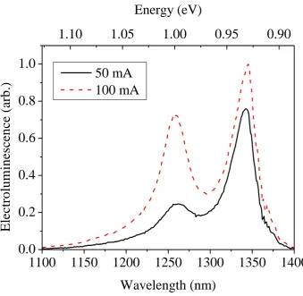
electroluminescence (EL) spectrum is shown in figure 1. It shows clearly resolved
room-temperature ground-state (GS) emission at EGS = 924.2 ± 0.1 meV and first
E = 60.3 ± 0.3 meV. For the IV measurements temperature control was provided by
mounting the samples in a closed cycle helium cryostat.
III. MEASUREMENTS
A. Switch-on voltage
The current I through a non-degenerate diode should scale exponentially as an applied
voltage is increased relative to the barrier potential. Here we investigate the diode
behavior well below threshold and monitor the “switch-on voltage” Von obtained at a
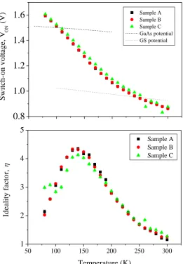
bias current of Ion = 2 mA for a range of temperatures. The results are shown in figure
3(a). The effect of series resistance was neglected since it is less than 2 Ω for these samples, resulting in an error of <4 mV, or less than 0.5 % of Von. The data show that
Von is close to the potential of the GaAs energy-gap of ~1.5 V (EGaAs/q) at low
temperatures, while above 150 K it falls towards EGS/q as it approaches room
temperature. We attribute the low-temperature value to non-thermalization of the dots
which in this instance act as mid-gap traps; captured carriers cannot escape but can
recombine resulting in some spontaneous light emission and the effective barrier is
that due to the GaAs matrix. The situation is reversed at room temperature where
carriers are constantly captured by the QDs but are also able to escape and thermalize
with the GaAs matrix, establishing quasi-Fermi levels that lie close to the dot GS. We
shall now show that the diode characteristic of the QD lasers can give further insight
into these details by offering a way to distinguish “trap-like” from “ideal” band
-to-band recombination.
The IV characteristics of a diode are usually described by the ideal diode
approximation as a function of I and the junction voltage Vj, where is the ideality
factor and IS is the saturation current, as shown in equation 1 [9]:
exp 1
B j S T k qV I I (1)
This equation can be derived analytically for some simplified cases but, in general, a
proper solution requires numerical calculation. However, it does provide a useful
empirical tool for analyzing experimental IV curves. The IV curve of a diode operated
in DC under forward-bias can be written as the series sum of Vj for an ideal diode and
the series resistance R as shown in equation 2, where V is the voltage measured at the
diode contacts. IR I I q T k IR V
V
ln 1
S B
j
(2)
Measuring in the presence of a series resistance R is known to be difficult, so we
have employed a current modulation measurement to extract [10, 11]. We chose to
measure d2V/dI2 because an Ohmic series resistance has no second derivative with
respect to current. To achieve this, the bias current was modulated with a
superposition of two sine waves at ~15 kHz and ~16 kHz. A lock-in amplifier then
measured the second-derivative of the IV curve by detecting the voltage response of
the diode at the difference frequency of 1 kHz. This frequency-mixing technique is
crucial in order to avoid harmonic distortion in the drive circuits, which would cause
the lock-in to measure a combination of the first and second derivatives. This is
particularly important since the second derivative falls off as 1/I 2, quickly becoming
small as the bias is increased, while the first derivative only falls off as 1/I. To ease
pre-factor –I 2, which allows small changes in the junction voltage to be identified. Applying this treatment to (2) gives (3), which, in the limit of IS << I, reduces to a
constant voltage signal.
q T k I I I q T k dI V d
I B II B
lim S
2 S 2 2 2 2 ) ( (3)
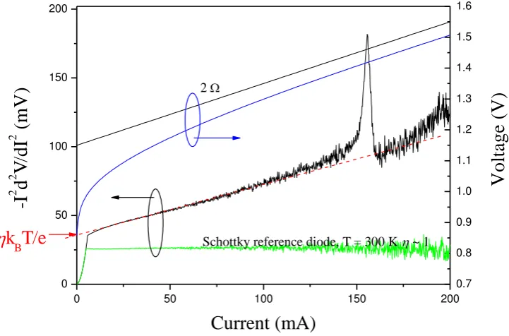
Figure 2 shows a –I2d2V/dI2 measurement obtained at room temperature from a reference Schottky diode and one of the QD laser diodes (sample A). Ignoring the
data obtained at very low currents, the Schottky diode exhibits a constant value of
mV q T kB 25
, consistent with an ideality factor ~1 as expected. The QD laser
diode shows more complicated behavior with a constantly rising background (which
we observe for all QD devices including those grown by other groups) and a peak
around 150 mA which coincides with the lasing threshold [12]. Here we extrapolate
the data to give an intercept voltage equal to kBT/q from which we can extract a
value for which is then used to indicate the detailed nature of the diode. Figure 3(b)
shows the temperature dependence of from 80 K to 300 K. At low temperatures
~2, consistent with “trap-like” recombination via the QDs, whilst at
high-temperatures tends to unity, consistent with thermalized band-to-band
recombination in the QDs. At intermediate temperatures, rises to a peak value of ~4
around 150 K. Such high values of have no obvious text-book interpretation but the
peak does imply that there is no monotonic transition from trap-like to thermalized
QDs and must involve an intermediate regime [13]. Remembering that QD lasers are
bipolar devices involving both electrons and holes carrier escape can occur in either
pair-wise fashion (geminate) or separately for each species (non-geminate). The
carrier-species, as has already been inferred from optical data [14]. To resolve this it
is necessary to analyze IS.
C. Saturation current
In an ideal diode, IS can be said to represent the diffusion current that would flow
across the diode junction at thermal equilibrium if it were not opposed by the built-in
electric field; it is often described as the theoretical reverse-bias leakage current (in
the absence of defects and shunt resistances) since, to a first approximation, the
diffusion current does not change under electric field. In the heterostructure
considered here, the high-bandgap AlGaAs barriers mean that there is negligible
diffusion across the junction compared to the thermally-generated carriers that escape
the intrinsic layer (in the form of electrons into the n-type side and holes into the
p-type side), therefore in this case we assume IS is entirely described by the thermal
generation and recombination of carriers in the active region. Specifically, we
consider it here as the net generation of carriers that can escape the active region
without recombining. Empirically, a small IS means a higher Von because the thermal
generation of carriers is smaller when the energy-gap is higher and conversely a high
IS means a small Von. IS can be estimated from the data by re-arranging equation (2) to
obtain (4), substituting the measured Von and , while again neglecting R.
1 exp
B on on S
T k qV
I I
(4)
IS, as deduced from Von and , is plotted in figure 4. The data suggests that below
150 K carrier escape is negligible and the QDs act as efficient traps for any electrons
and holes in the active region, so carrier recombination dominates over generation,
resulting in a small IS. In this regime, carriers captured from the GaAs matrix by the
recombination from a thermalized carrier population in the GaAs matrix. As the
temperature is raised through the transition region of high , IS rises sharply to a peak
at ~190 K and then falls as the temperature is further raised. We attribute this to the
non-geminate escape of holes and electrons. The lower confinement of the holes
allows them to escape at lower temperatures than the electrons, leading to the rise in
IS with temperature seen in figure 4, as more of the thermally-generated carriers
become able to escape the active region. These holes do not recombine in the active
region because of the low availability of electrons, which are still efficiently trapped
by the QDs. As the temperature is raised further and the electrons are able to escape,
the active region is populated with both electrons and holes, as a result the
thermally-generated carriers are able to recombine before leaving the junction region, causing IS
to drop with further increases in temperature.
IV. EFFECTIVE BARRIER HEIGHT
At this point, the expectation that the holes escape at lower temperatures than the
electrons is purely based on their lower confinement energy compared to that of the
electrons [15, 16]. We will now proceed with a more detailed analysis of IS and in
an attempt to gain more quantitative insight, by using these parameters to infer the
“effective” barrier height of the diode junction. An effective barrier height would
describe the rate-determining potential barrier within the diode, as opposed to the
overall potential barrier Von (similar to differential resistance as opposed to pure
Ohmic resistance). To estimate this quantity from the data in figure 4, we note that
qVon/ is always significantly larger than kBT allowing equation (4) to be
approximated as (5):
T k qV I
I
B on on
Equation (6) can then be substituted into the ideal diode equation (1) to give (6). This
suggests that the switch-on voltage divided by the ideality factor specifies the size of
the rate-determining potential barrier.
T k
qV qV
I I
B on j
onexp
(6)
Therefore, a diode requires a voltage of the order of Von to conduct but the variation of
current, for a change in applied voltage, is determined by the smaller term qVon/ . In
an ideal Schottky diode (=1) recombination occurs with no internal structure to the
process (i.e. pure band-to-band), so a higher gives details of any internal structure to
the recombination pathways of the non-degenerate diode. For instance, the limiting
case of Shockley-Read-Hall (SRH) recombination involves a mid-gap state which
must alternatively capture electrons and holes to achieve interband recombination. In
this case, the presence of the mid-gap trap state halves the rate-determining potential
barrier compared to the ideal case and this gives = 2. SRH theory thus gives ideality
factors between 1 and 2 depending on the balance of rates between ideal and
trap-mediated recombination. Diodes with > 2 have frequently been reported, especially for wide bandgap materials such as GaN and ZnO, and has been attributed to coupled
defect levels [17], variation in Schottky barrier height [18, 19], the combination of
ideality factors of a series of diode junctions within a structure [20, 21] or localized
(Frenkel-Poole) conduction in amorphous layers or at interfaces [22].
The results of this analysis are plotted on an Arrhenius scale in the inset to figure 4
and the trend in qVon/ can be fitted with the sum of two Arrhenius-like dependencies
T k E B T k E A qV B 1 B 0
on exp exp
(7)
Below 160 K, qVon/ reduces with activation energy E0 = 15.2 ± 0.1 meV, while at
temperatures above 160 K it rises with activation energy E1 = 58.3 ± 0.8 meV (the
actual slope of the trend being E1 - E0 = 43.1 meV in this region). The energy-splitting
of the GS and X1 emission is believed to be shared between the electrons and holes
with a band offset ratio of ~2.5:1 [16, 23-24], respectively, giving an expected
electron-state spacing of EE ~ 43 meV and a hole-state spacing of EH ~17 meV;
from previous optical studies this spacing is consistent amongst the first few
confined-states of the QDs [15, 16]. We attribute E0 and E1 to the activation energies required
for scattering between the hole states (E0) and both the electron and hole states (E1) in
the QDs. The use of Arrhenius relations in fitting the data is justified by assuming the
behavior of the diode junction is determined by the rate of intradot carrier scattering
between the confined-states. We believe this presents strong evidence that the high
ideality factor in the “intermediate regime” is due to the separate escape of holes at a
lower temperature than the electrons.
V. CONCLUSION
By comparison of the temperature dependence of the switch-on voltage, ideality
factor and saturation current behavior of InAs/GaAs QD bilayer laser diodes with
ideal diode behavior, it was found that the quasi-Fermi levels of the diodes are
associated with the GaAs/WL continuum states at low temperatures, but drop into the
QD confined-states as carrier escape becomes possible at higher temperatures and
carrier thermalization occurs. A peak in the ideality factor around 150 K suggests that
the transition from “trap-like” recombination at low temperatures to thermalized
that the ideality factor of the QD diode can be interpreted in terms of internal structure
to the recombination pathways and thus the rate-determining barrier within the QD
junction can be analyzed. We have proposed a physical model to explain the barrier
energy in terms of the rate-determining processes being: (a) one-way carrier capture
into the QDs at low temperature, (b) partial thermalization of the holes only near
160 K and (c) interband recombination across a thermalized QD GS at
References
1. D. J. Mowbray and M. S. Skolnick, J. Phys. D: Appl. Phys. 38, 2059 (2005)
2. M. Asada, Y. Miyamoto, Y. Suematsu, IEEE J. Quantum Electron. 22, 1915
(1986)
3. Y. Arakawa, H. Sakaki, Appl. Phys. Lett. 40, 939 (1982)
4. H. D. Summers, J. D. Thomson, P. M. Smowton, P. Blood, M. Hopkinson,
Semicond. Sci. Technol. 16, 140 (2001)
5. I. O’Driscoll, P. M. Smowton, P. Blood, IEEE J. Quantum Electron. 45, 380 (2009)
6. I. O’Driscoll, P. Blood, P. M. Smowton IEEE J. Quantum Electron. 46, 525
(2010)
7. E. C. Le Ru, P. Howe, T. S. Jones, R. Murray, Phys. Rev. B 67, 165303 (2003)
8. E. Clarke, P. Howe, M. Taylor, P. Spencer, E. Harbord, R. Murray, S.
Kadkhodazadeh, D. W. McComb, B. J. Stevens, R. A. Hogg, J. Appl. Phys. 107,
113502 (2010)
9. S. Sze, K. K. Ng, “Physics of Semiconductor Devices”, Wiley-Blackwell (2006) 10.T. L. Paoli, IEEE Trans. Electron. Devices 23, 1333 (1976)
11.T. L. Paoli, J. F. Svacek, Rev. Sci. Instrum. 47, 1016 (1976)
12.P. Spencer, E. Clarke, P. Howe, R. Murray, Electron. Lett. 43, 574 (2007)
13.S. Sanguinetti, M. Henini, M. Grassi Alessi, M. Capizzi, P. Frigeri, S. Franchi,
Phys. Rev. B 60, 8276 (1999)
14.E. C. Le Ru, J. Fack, R. Murray, Phys. Rev. B 67, 245318 (2003)
15.R. J. Warburton, C. S. Dürr, K. Karrai, J. P. Kotthaus, G. Medeiros-Ribeiro, P. M.
Petroff, Phys. Rev. Lett. 79, 5282 (1997)
16.B. N. Murdin, A. R. Hollingworth, J. A. Barker, D. G. Clarke, P. C. Findlay, C. R.
Pidgeon, J.-P. R. Wells, I. V. Bradley, S. Malik, R. Murray, Phys. Rev. B 62,
R7755 (2000)
17.A. Schenk, U. Krumbein, J. Appl. Phys. 78, 3185 (1995)
18.E. H. Rhoderick, R. H. Williams Metal-Semiconductor Contacts (Oxford
University Press, Oxford, 1988)
19.S. Chand, J. Kumar, J. Appl. Phys. 82, 5005 (1997)
21.C.-X. Wang, G.-W. Yang, H.-W. Liu, Y.-H. Han, J.-F. Luo, C.-X. Gao, G.-T.
Zou, Appl. Phys. Lett. 84, 2427 (2004)
22.M. Brötzmann, U. Vetter, H. Hofsäss, J. Appl. Phys. 106, 063704 (2009)
23.R. J. Warburton, B. T. Miller, C. S. Dürr, C. Bödefeld, K. Karrai, J. P. Kotthaus,
G. Medeiros-Ribeiro, P. M. Petroff, and S. Huant, Phys. Rev. B 58, 16221 (1998).
24.M. Fricke, A. Lorke, J. P. Kotthaus, G. Medeiros-Ribeiro, and P. M. Petroff,
Table I
E0 (meV) E1 (meV)
Sample A 19.4 ± 0.3 48.7 ± 0.8
Sample B 16.8 ± 0.2 60.1 ± 0.9
Sample C 9.3 ± 0.2 66 ± 2
Figure Captions
Table 1: Activation energies E0 and E1 for samples A, B and C; we attribute E0 and
E1-E0 to the energy spacing between the confined hole and electron states,
respectively, within the QDs.
Figure 1: Electroluminescence spectrum of the QD bilayer laser below threshold at
room-temperature. The GS emission peak is at 1341 nm and the X1 emission peak is
at 1259 nm; the GS and X1 emission is separated by 60.3 ± 0.3 meV.
Figure 2: An example IV curve and –I2d2V/dI2 spectrum of the QD laser diode. While
the latter is different from the expected form of an ideal diode (e.g. the Schottky diode
shown as a dotted line) diode, there is still a clear intercept voltage from which the
ideality can be deduced.
Figure 3: (a) The temperature dependence of the switch-on voltage. At low
temperatures it is close to the GaAs bandgap potential, while near room-temperature it
is associated with the QD GS energy. (b) The temperature dependence of the ideality
factor, extracted from the current modulation measurement. The ideality factor is high
at low-temperature, peaking near 150 K before dropping towards unity at high
temperatures.
Figure 4: IS calculated from VON and . It is suppressed below 150 K because of the
efficient capture of carriers into the non-thermal QD states, while at higher
temperatures it is thermalized. (Inset) Arrhenius plot of the estimated rate-determining
Figure 1
1.10
1.05
1.00
0.95
0.90
1100
1150
1200
1250
1300
1350
1400
0.0
0.2
0.4
0.6
0.8
1.0
E
le
ctr
o
lu
m
in
es
ce
n
ce
(
ar
b
.)
Wavelength (nm)
50 mA
100 mA
Figure 2
0 50 100 150 200
0 50 100 150 200
0.7 0.8 0.9 1.0 1.1 1.2 1.3 1.4 1.5 1.6
-I
2
d
2V
/dI
2
(
m
V
)
Current (mA)
2 V
o
lt
ag
e
(V
)
k
Figure 3
0.8
1.0
1.2
1.4
1.6
Sample ASample B Sample C GaAs potential GS potential
S
w
it
ch
-o
n
v
o
lt
ag
e,
V
ON
(
V
)
50 100 150 200 250 300
1 2 3 4 5
Sample A Sample B Sample C
Id
ea
li
ty
f
ac
to
r,
Figure 4
50 100 150 200 250 300
10-39 10-33 10-27 10-21 10-15 10-9
2 4 6 8 10 12 14
250 300 400 500 600 700 800 900 1000
Sample A Sample B Sample C
E
sti
m
ate
d
I
S(
A
)
Temperature (K)
qV
ON
/
(
m
e
V
)