This is a repository copy of Modelling RF interference effects in integrated circuits.
White Rose Research Online URL for this paper:
http://eprints.whiterose.ac.uk/99090/
Version: Published Version
Proceedings Paper:
Whyman, N. L. and Dawson, J. F. orcid.org/0000-0003-4537-9977 (2001) Modelling RF
interference effects in integrated circuits. In: Electromagnetic Compatibility, 2001. EMC.
2001 IEEE International Symposium on. IEEE , 1203-1208 vol.2.
https://doi.org/10.1109/ISEMC.2001.950603
[email protected]
https://eprints.whiterose.ac.uk/
Reuse
["licenses_typename_other" not defined]
Takedown
If you consider content in White Rose Research Online to be in breach of UK law, please notify us by
Modelling
RF interference effects in Integrated Circuits.
N.
L. Whyman
DERA (Farnborough)
Hampshire, GU14
OLX(UK)
Abstract: The disturbance effects in complex electronic systems, subjected to a High Power Microwave (HPM), Continuous Wave (CW) or Pulse irradiation, show a conversion of the injected High Frequency (HF) out-of-band signal to a Low Frequency (LF) inband signal. In this paper a behavioural model is presented that combines HF and LF subcircuits to predict the effect of Radio Frequency Interference (RFI) on linear integrated circuits. The model is constructed from detailed measurements and manufacturers’ data, and can be used to determine the upset mechanism in analogue systems subjected to RFI.
Summary
The electromagnetic (EM) environment in which electronic systems have to operate is becoming increasingly hostile while dependence on electronics is widespread and increasing. The need for assurance that upsets due to the EM environment will not occur is fundamental to acceptance of systems as fit for purpose. Design features to impart EM hardness are beginning to be implemented ab initio’, but hardness verification of major systems still depends on testing prototype hardware late in the development process. This is expensive, and the cost of rectification of any shortfall found can be enormous.
Modem equipment design and evaluation processes are increasingly being carried out using computers. CAD/CAE systems are now being used extensively in industry for design and manufacture in a number of disciplines - aerodynamics, structures, mechanical, and of course, electronic design. The elements exist in principle to treat EM hardness in the same way. This opens the prospect of the hardness (or vulnerability) of a virtual design (CAD files) being amenable to virtual evaluation using modelling and a knowledge base. Virtual clearance of the system via the endorsement of the design and evaluation processes, to the satisfaction of a clearance authority, is the ultimate goal. While these may be long term objectives, addressing them now will produce substantial benefits in the short term including problem identification, decomposition of large-scale testing and a better general understanding of the RFI effects on systems.
The elements to allow software evaluation of EM hardness are coupling modelling and circuit emulation. Both of these have a substantial history, but neither has been developed to the stage where it can be used for practical hardness evaluation. A third element - a knowledge base (e.g. reactions of non-microwave semiconductors to microwave frequency inputs and of the practicalities of implementing coupling models) is required if such a process is to become reality. An integrated process has yet to be demonstrated.
Much work has been done to characterise the effects of electromagnetic interference on operational amplifiers and other
Far preferable to “bolt-on fixes” later on
J. F. Dawson
Dept.
of
Electronics, Universityof
YorkYork, YO10
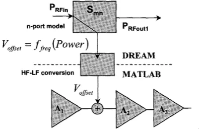
SDD(UK)circuits [l ] [2]. Little attention has been given to addressing the problem of a system with more than one element (i.e. op-amp). This paper presents a means of modelling such systems. The model consists of a linear model to represent the interference propagation (HF subsystem) and a non-linear tkequency dependent function to generate offset voltages that are injected into the LF part of the model, which can use standard device (macro) models, as illustrated in Figure 1 [3].
[image:2.612.329.529.272.402.2]n-port
Figure 1 Two-layer model showing coupling between HF and LF layers
To implement this model, according to Figure 1, two different data analysis tools were used; DREAM and Mathworks MATLAB. DREAM is a database with an interface to MATLAB used by EMH&P group DERA to store and process laboratory data. DREAM was used to define the HF n-port model and MATLAB derives the HF-LF conversion to enable the calculation of the voltage offset to RF power levels. This works under the main circuit analysis tool such as PSpice. Other methods of data analysis can be used with the model, which may be to be implemented using any of a wide range of software tools method.
The HF subsystem is characterised by linear s-parameter measurements using an IC test jig and a Network Analyser (NA)
[4].
This subsystem can be modelled directly in the frequency domain by a circuit simulator program such as PSpice. Coupling of interference between different pin configurations was modelled and the results compared with measured data. To verify the behavioural model for the comparison of measurements and simulation, an amplifier was set-up as a voltage follower buffer, modelled and compared to the measurements, from lOOMHz to 6GHz. In this circuit the RF+
dc biasing is fed back into pin 2 of the device in a conventional buffer configuration as illustrated in Figure 2.there are discrepancies between the calculated and the measured data. Some discrepancies at the higher frequencies in all the validation set- ups do show limitations of the model andor measurements, which must be further, analysed.
[image:3.613.101.292.134.250.2] [image:3.613.320.536.209.348.2] [image:3.613.85.302.300.433.2]Level indicated on graph
Figure L ldeasurement and simulation of an amplifier co...igured as a voltage follower gain 1 showing the Bias T fitted to isolate test fixture from Network Analyser
Drive level
n, A
Low
.I
t
-10dBm
. . . .
.
.. ~.. . . . .
-1 0
m -15
m
E
-206 -25
-30
-35
-measurement -40 -simulation
Frequency Hz
Med.
I
O a m IMid [ l a m
I
Table 1 network analysers drive power levels
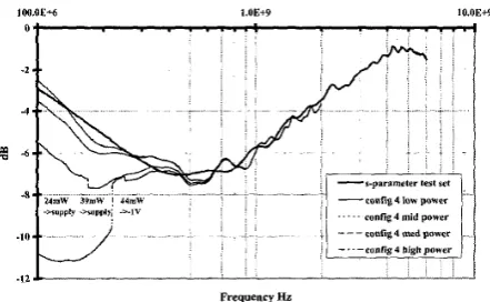
It is significant that the measurements carried out on pins 2, 3, 6 and 7 (Figure 4) show no large change in their scattering measurements. However in the case of pin 4 (negative power supply rail) significant changes in its scattering parameters can be seen as the input power is increased (Figure 5). The reason for this change is not known at present. However, the power level for which the change occurs is sufficiently high that this effect can be assumed not to be relevant under expected operating conditions.
-10
3
-15
-20
-25
[image:3.613.319.540.400.536.2]Frequency Hz
Figure 4 Effect of variation of input power on pin4 S21 -ve supply to pin7 +ve supply
1.OEt9 10.OE+9
’LA--
-
--s-pararneter test seteonfig 4 low power
config4 mid power ~ “ P P l Y -supply, % l V
eonfig4 med power
-1 2
)
’
Frequency Hz
Figure 5 Effect of variation of input power on pin4 S11 -ve supply showing upset at power levels
-
supply means f 12VThe results indicate that the
RF
transmission or propagation is generally due to the device and packaging parasitic. This illustrates an important result since the propagation of RFI through a device seems to be independent of the detail and function of the internal structure of the chip. The results suggest that it may be possible to use circuit analysis programs to predict the effects, in both linear and digital ICs, of RF voltages incident on the pins of the device, without detailed knowledge of the internal structure of the chip. In this paper a model will be illustrated and discussed that will use measurement data to define the transfer functions, between all the pins on the device. This enables the synthesis of a linear model to define thedevice propagation characteristics to frequency and time domain RFI waveforms. This is illustrated in Figure 6, and will be used to define the HF model used in this paper.
Devlce conflgutafion = 5 4 4
' O
m lo Lbondwire - inductance d m lo
me IC bondmre
Cpad - capacitance due tu me pad and d?e suosbate Din b 1
[image:4.615.328.542.80.237.2]Pin 7
Figure 6 model definition for the transfer function and input impedance between all the pins on the device
Experimental validation of the HF linear model
This part of the paper will define the methodology of the model to evaluate the input impedance and the cross coupling of RFI between the individual pins, according to the model described in Figure 6. To define the input impedance and the coupling or transfer function, measurements were carried out according to [5].
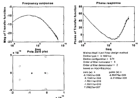
To design a model to define the device transfer function a method has been designed to use a least-mean-squares 'best fit' filter using the measurements. The method is based on a novel application of the Wiener-Hopf equation for signal estimators as described in [8], with the same method described by Levy [9] and used in the Matlab 'Signal processing toolbox' routine 'invfi-eqs' according to reference [lo]. The transfer function of the device can be described as a ratio of polynomials in s, which can be used to determine the time, or frequency response of the device by means of Laplace transforms. The transfer function is of the form
Zeros zsi Poles psi
-5.9735e" -3 .0239e9
-6. 1997esk4.2634e10i
-9.3649e9f3.1303e"i
-1.249e"
4.493 le"f1 .0208e1'i The values a,, and b, are coefficient multipliers.
The graphs and the pole zero plot indicate the frequency and phase response of the device and will define the transfer function for each pin according to the next set of figures.
F r e q u e n c y r e s p o n s e
i r e q
lo'o P o l e Zero p l o t
:pi
5 -6 -4 -2 0 2
x 1 O'O
-1501 I
1 on 1 OP 1 O ' O freq
Weiner-Hopfl Lew F~Iter design method Deuce type = $c 11061cp
D d e r Of lilter numerator = E Order of filler denominator = 1
bared on H(rI=B(o)IA(a) zem (4 =
-5.97352er010 -3 02359e+O09
-6 119E7er006 -6 11967e+006 -9 3548Ee+009 -9 36465e+009 -1 2494e+010 4493110+009 449311e!+009
Device con6g"ratlon = SI,
poles [Wl =
Figure 7 Wiener-Hopf algorithm applied to the device thick line measurement SI1 for pin 7 with the dotted line the curve fit
P h a s e r e s p o n s e F r e q u e n c y r e s p o n s e
Order
Order of of filler fllfsrdenomlnaloi numerator = i 9 1 bared on H(s)=B(r)lA(a)
4 830Eer009 -1 0243et009
zero (W) = polel (W)
-
4 6306er009
6 02823e+OO9
6 02823er009
-1 059EEer040
5 ' I
x 10'O
2 1 0 1 -1 059EEet010
5 5058+009
2 52373er009
[image:4.615.94.274.111.224.2] [image:4.615.324.548.275.433.2] [image:4.615.82.301.509.665.2]-1 ~ . 2 2 a 3 ~ + o i o
Figure 8 Wiener-Hopf algorithm applied to the device thick line measurement Sll for pin 4 with the dotted line the curve fit
P h a s e r e s p o n s e F r e q u e n c y r e s p o n s e
40
E 20
lorn
= : o .20 1 o8 1 os 1 O'O
f r e q Weiner Hopf I Le* Filter d e W n method Deuce type = IC 11061cp Deuce configuration = 574
order of mer numeralor - 5 Order of filter denominator = 2 bared on H(s)=B(S)IA(s) l 0 1 O P o l e
2 2
p l o tzero [W) = pole* (W) i
8 1 0 4 5 w a a 8 8 ~ 6 4 7 6 ~ r a w
8 ? a w e + o m ~ 2 i z 6 6 ~ + 0 0 8
159fflet010 15911le+Of0 725527e.007
2 1 0 1
x l 0 ' O
Figure 9 Wiener-Hopf algorithm applied to the device thick line measurement SZl between pin 7 and 4 with the dotted line the curve fit
For pin 7
-+
4 the transfer function in s isH(s) =
To implement a circuit model from the transfer function the poles and zeros of the function have to be obtained by factorisation of the quadratics in s-plane form by and displayed in Table 2 and Table 3
Pin 14 Zeros zsi Poles psi -8. 1045e8+4.6304e10i -8.8648e9
-8. 1045e8-4.6304ei0i -9.2127e8
-1.591 le10+1.9897e10i
-1.591 le10-1.9897e10i
7.2563e7
This model can be implemented into PSpice using the Laplace Transform (LAPLACE) part.
For large modem devices, the measurement of individual pins will be
difficult as the number of measurements on an n pin chip is n
+
n .For an 8-pin device we require 72 measurements, for a modern 128- pin device we require 16512 measurements. Another approach is required and a possible solution will be discussed in the next part of the paper.
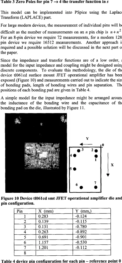
Since the impedance and transfer functions are of a low order, a model for the input impedance and coupling might be designed using discrete components. To evaluate this methodology, the die of the device t106 1 cd surface mount P E T operational amplifier has been exposed (Figure 10) and measurements carried out to indicate the size of bonding pads, length of bonding wires and pin separation. The positions of each bonding pad are given in Table 4.
A simple model for the input impedance might be arranged around the inductance of the bonding wire and the capacitance of the bonding pad on the die, illustrated by Figure 1 1.
Pin 14 Zeros zsi Poles psi
-8. 1045e8+4.6304e10i -8.8648e9
-8. 1045e8-4.6304ei0i -9.2127e8
-1.591 le10+1.9897e10i
-1.591 le10-1.9897e10i
7.2563e7
0
[image:5.612.74.295.76.175.2]I.
s - l l aFigure 10 Device tl06lcd smt JFET operational amplifier die and pin configuration.
0.3pF Rbondvire L7
The inductance of the bond wire may be estimated by considering it as half a circular loop:
Bondpad Capacity
(3)
I 4pF
where R is the radius of the loop formed by the bond-wire, a is its radius, and p is the permeability of the medium in which the loop is embedded. The radius of the bonding wire for this technology is 12.5pm and the length of the bond-wire 1 is 1.5-2.5mm giving a loop radius of 0.48-0.8mm. Taking p = b this gives an inductance in the range 1.1-2.lnH.
To calculate the input capacitance of the device, if we assume that the pad forms a simple parallel plate capacitor, and ignore fringing effects:
A C = & & -
" d (4)
where A is the area of the pad, d is the dielectric thickness, is the permittivity of free space and 5 is the relative permittivity of the dielectric.
The thickness d for this type of technology is 0 . 5 ~ and the E, has a value of 4 for SiOz. The pad size is approximately 0.24Omn-1, giving a capacitance of 4pF. This model does not take in to account the effect of the device lead ffame, which will need further investigation. A simple illustration of this model is illustrated in Figure 11.
Lbond wire Device parasitics
[image:5.612.69.302.174.676.2]Si
Figure 11 configuration device input characteristic impedance
We also include the series resistance of the bond-wire and a resistor to represent the loss in the silicon, and a parasitic capacitance from the pin to bad in the equivalent circuit shown in Figure 12.
Figure 12 PSpice implementation of the Sll value of the device using values equated from equation (1) and (2) to configure pin 7 (positive power rail)
Figure 13 illustrates the comparison of the calculated device parasitics used in the simulation and the measured device scattering parameter SI1 according to the measurement system in [3].
I " I I I
Table 4 device pin configuration for each pin
-
reference point 0located at bottom right of die.
[image:5.612.372.488.324.409.2] [image:5.612.72.291.390.540.2] [image:5.612.343.519.471.583.2]Figure 13 Comparison of the calculated device parasitics used in simulation and the measured device scattering parameter SI1 for pin 7 of the modelled device.
...
-12v
From this approach the input impedance might be modelled using die measurements. The main future research will be to define the pin-to- pin coupling algorithm to enable an analytical method for the transfer function derived from die measurements and semiconductor physics. Manufacturers IBIS models may also provide some insight into pin properties of unknown IC.
Non-linear parameter measurement
A test circuit has been developed to determine the validity of the non- linear model. The circuit, Figure 14, is an amplifier with a feedback factor,
j3,
which is used in a number of configurations. This was designed around the device test jig described in [3]. The amplifier configurations used are a Voltage follower, a Non-inverting Amplifier, and an Inverting Amplifier. The tests are carried out using a dc Voltage input(Vi)
of zero or 200mV which remains constant over the full test.The amplifier configurations are based on
&,
-
closed loop gain of the amplifier and a schematic where Rf and Ri are the resistors for feedbaik and input respectively1
Voltage follower Ad(VF) =
-
=P
Non-inverting Amplifier A,I(N~) = 1 = 1
+
-
R f R i Calculations based on&l(NI) = 5 Rj = 4.7w1 R f = 18.8kQ
&IN) = 22.3 Ri = 4.7162 R f = l O O w 1
...
0 6 6 0
Figure 14 Configuration of Amplifier circuit used.
50
The
RF
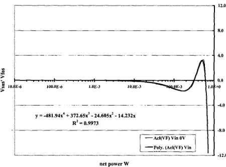
induced voltages to be used in the LF subsystem, can be derived from direct measurements carried out on the device and used to determine the offset as set of polynomial functions of frequency and incident power or voltage [3]. This is illustrated in Figure 15.0.0 llM.OE-6 1.OE-3 IO.OE-3 E 3 1.0 to
y = - 4 8 1 . 9 4 ~ ~ + 372.65.' - 24.605~' - 14.232~
R'
-
0.9973I I
-12 0
-
-- ___ ___ -___
__ __ -net power W
Figure 15 Comparing measured offset voltages and the polynomial approximation of offset voltage with net power for
RF injection into Pin 7 of device tl06lcp amplifier at 250MHz.
These can be derived by measuring the offset voltage due to the RF against the net RF power levels where Vf,, is a function of fkequency and power. The non-linear equation can be calculated using an nth order polynomial curve fitting routine. Therefor, pin 7 @ 25OMHz
for input Voltage of constant zero Volts, the equation will be:
VfOs = -481.94P,4,, +372.65P,, -24.605P,2,, -14.232Pnet (7)
The offset voltage is implemented by injecting an input voltage due to the RF Vios into the LF model at the input to the amplifier as shown in Figure 16.
,
Vios
Vfos -
I
I
I
I
Figure 16 simple configuration of an amplifier A with a feedback of pwhere Vios is input Voltage due to RF and Vfos
RF
induced offset voltage outputConsidering the effect of the input offset on the amplifier output:
Vfos = Avios - APVfos
(1 + AP)Vfos = AVios
(10) A
Vfcls =-
1 +AB vi's
Vios
Vfo, =
-
P
From Equation (11) we can make the assumption that we do not require to know the open loop gain A of the device to determine or model the input offset parameter.
If the amplifier equation is included to equation (1 1)
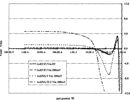
Figure 17 illustrates the correct assumptions made by equation (12) that the derived output voltage is based on Vi plus Vfos using the circuit described in Figure 14.
8.0
4.0
0.0
.+O
4.0
4 . 0
net power W
Figure 17 Measured offset voltages using different amplifier gain configuration based on equations (11) and (12).
Conclusions and discussions
The approach presented allows the possibility of predicting the propagation and effect of interference in electronic systems. By the use of a two-level model avoids the difficulty in simulation of the wide disparity in the frequency ranges of out-of-band interference and the operating signals in the circuit. A new method of modelling the Radio Frequency Interference effects on analogue circuits has been presented that incorporates the following features:
the model uses a synthesis of a Laplace transfer function or lumped model to represent a subcircuit that describes the input impedance and the radio frequency propagation through the device. This is illustrated by Figure 3 and shows close agreement between the calculated and measured data
a non-linear frequency dependent function to generate offset voltages that are injected into the LF part of the model. Simple polynomial functions Figure 15 (7) have been devised, fiom measurements, to give the correct response on the device from the frequency and power levels of the injected RF.
The method described here could be developed to model the propagation and effect of EM1 in systems, whether analogue or digital. Work has been carried out on IC immunity measurements to look at standardisation of RF power levels to upset criteria [ 1 13. The linear propagation model might be used just as a golno-go detector
comparing the power levels from PSpice simulation to this upset criterion for the device i.e. is the RF level on this pin above a susceptibility threshold for upset.
The linear subsystem could be simply interfaced to numerical electromagnetic models to determine its level of susceptibility due to interference from external electromagnetic fields. Numerical electromagnetic tools can be used to determine the induced voltage sources on and s-parameters of PCB tracks and interconnections. These can be combined with the device models to predict interference levels at any node in a system.
References
James J. Whalen, “Predicting RFI Effects in Semiconductor Devices at Frequencies above IOOMHz” IEEE Transactions on Electromagnetic Compatibility, Vol.EMC-21, No.4, pp. 281-
282, November 1979.
J.F. Dawson, W. Persyn, S. Hagiwara, and J. Wood, “The need for macro-models in the simulation of EMI effects in integrated circuits”, EMC’94 ROMA, Rome, 13-16‘h Sept 1994, pp. 638- 643.
N. L. Whyman, J. F. Dawson, “Two level, in-bandout-of-band modelling RF interference effects in integrated circuits and electronic systems”, IEE 1 lth International conference on EMC. (IEE Pub. 464), York, 12-13‘h July 1999, pp. 135-139.
N. L. Whyman, “Modelling RF interference effects in integrated circuits and electronic system”, M.Phil. to D.Phil. transfer report submitted to University of York 1999.
N. L. Whyman, J. F. Dawson and A. Centeno, “Verification of a behavioural model to define RF interference effects in integrated circuits”, York EMCOO.
N. L. Whyman, J. F. Dawson, “Two level, in-bandout-of-band modelling RF interference effects in integrated circuits”, EUROEM 2000, Euro Electromagnetics, Edinburgh, 30th May -
2nd June 2000
J. Bohl, T. Ehlen, F. Sonnemann, N. Whyman, “Methodology and Results of System Simulation from the Farfield to Circuit
Level at HPM Radiation”, EUROEM 2000, Euro
Electromagnetics, Edinburgh, 30” May - 2nd June 2000
B Widrow and S. D. Streams, “Adaptive signal processing”, Prentice-Hill, 1985, ISBN 0-13-004029-01, pp. 250-264.
E. C. Levy, “Complex curve fitting”, IRE Trans. on Automatic Control”, AC-4:37-44, 1959.
[IO] J. A. Cole, J. F. Dawson, S. J. Porter, “A digital filter technique for electromagnetic modelling of thin composite layers in TLM’,
[ 111 European Aircraft EMC Research Group.
Acknowledgements
The authors wish to thank the Technology Group 07 of the UK MOD Corporate Research Programme for their support during this research project.
0
British Crown Copyright 2001I
DERA
Published with the permission of the controller of Her
Britannic Majesty’s Stationery Office.
[image:7.612.73.301.219.394.2]