Article
Nano-Structured Gratings for Improved Light
Absorption Efficiency in Solar Cells
Farzaneh Fadakar Masouleh1,2,*, Narottam Das3and Seyed Mohammad Rozati1
1 Science Faculty, Department of Physics, University of Guilan, Rasht 41938-33697, Iran; [email protected] 2 School of Engineering and Computer Science, Victoria University of Wellington, P.O. Box 600,
Wellington 6140, New Zealand
3 School of Mechanical and Electrical Engineering, University of Southern Queensland, Toowoomba, QLD 4350, Australia; [email protected]
* Correspondence: [email protected]; Tel.: +98-131-322-0912
Academic Editor: Peter V. Schaeffer
Received: 22 July 2016; Accepted: 2 September 2016; Published: 19 September 2016
Abstract:Due to the rising power demand and substantial interest in acquiring green energy from sunlight, there has been rapid development in the science and technology of photovoltaics (PV) in the last few decades. Furthermore, the synergy of the fields of metrology and fabrication has paved the way to acquire improved light collecting ability for solar cells. Based on recent studies, the performance of solar cell can improve due to the application of subwavelength nano-structures which results in smaller reflection losses and better light manipulation and/or trapping at subwavelength scale. In this paper, we propose a numerical optimization technique to analyze the reflection losses on an optimized GaAs-based solar cell which is covered with nano-structured features from the same material. Using the finite difference time domain (FDTD) method, we have designed, modelled, and analyzed the performance of three different arrangements of periodic nano-structures with different pitches and heights. The simulated results confirmed that different geometries of nano-structures behave uniquely towards the impinging light.
Keywords: solar cell; photovoltaic cell; FDTD modelling; subwavelength nano-structures; reflection loss
1. Introduction
Given the economic and environmental incentives, and the resulting paradigm shift towards a more sustainable development, producing clean energy is becoming increasingly important, where PV systems development is one of the fastest growing industries. Solar cells or photovoltaic (PV) systems, categorized in solid state electrical devices, have been suggested to provide a clean alternative method for generating electricity from sunlight. They attracted a lot of attention due to viability, reliability, and accessibility especially in the remote areas even in satellite systems [1]. The Compound Annual Growth Rate (CAGR) of PV installations was reported to be 44% between 2000 and 2014 [2]. However, the performance of solar cells is still far from a satisfactory level. Ongoing research towards enhancing the generation of clean electrical energy is focused on improving the functionality of solar cells. Studies towards optimization of PV cells are mainly about construction of more efficient and flexible PV cells, allowing for easy installation and transportation.
Solar cells convert sunlight into DC voltage due to the PV effect [3]. Subsequently, the generated DC electricity is transformed into AC source via a converter and thus it can be introduced to various systems for applications. Furthermore, transformation of solar energy to chemical energy can be performed by a PV cell named photoelectrolysis cell (PEC) which uses photon energy to split water [4,5].
Absorption of the illuminated sunlight results in the creation of electron and hole (e-h) pairs which are later separated under influence of an internal electric field. Generally, PV cells are composed of layers of semiconductor materials, conventionally silicon in its different crystalline forms, i.e., mono- or multi- crystalline. While the crystallized silicon does not show promising electric conducting behavior, selectively contaminating the semiconductor with a controlled level, namely doping, helps to generate a good amount of electric current [6,7]. Usually, the top and bottom layers of the PV cell are doped with boron and phosphorus to enable negative and positive charge generation, respectively [8].
An individual square cell averaging about four inches on each side is only able to produce a small amount of power, and due to its small size, once it is exposed to harsh environmental conditions, it might fail to function properly. Thus, interconnected solar cells are usually grouped together and designed in series to form modules for commercial usage. Furthermore, bigger units called solar panels and solar arrays can be assembled in groups or used individually. The panels and arrays are usually protected with glass or plastic front covers against environmental threats to eliminate potential damages [9].
Second generation solar cells, which benefit from relatively newer manufacturing technologies, are a thin film solar cell group which is developed by depositing layers of thin films on a substrate [10]. The deposited material is not confined to silicon and this method is growing rapidly due to relatively easy mass production capability, flexibility to work under different situations, and fine performance under high temperatures.
Regardless of the advantages of thin film solar cells, it has been argued that the alternative technologies used for the development of second generation solar cell design do not achieve a better efficiency compared with the first generation. Therefore, the technology of third generation or next generation solar cells was introduced which includes thin film solar cells combined with organic [11,12], polymer [13], dye-sensitized [14–16], nano-structures, and nano-structured interfaces, i.e., nano-wire/particle or quantum dot solar cells [17–20].
There are several environmental parameters affecting solar cell performance, such as geographical latitude, seasons, weather, position, and the sunlight’ s angle of incident [21–23]. However, it is fundamental to study the characteristics of PV systems from a basic point of view. These include parameters which have direct relation with the material composition and physical design of the PV cell which ultimately enable the device to collect or welcome more sunlight.
The choice of material for nano-structures in solar cell design is broad, and PV industry is facing challenges to achieve the best efficiency [24–26]. Hence, it is useful to design solar cells with specific geometries to benefit from some interesting characteristics, e.g., using metallic and semiconductor nano-structures can cause extraordinary optical transmission for light localization [27–29]. Using metals to build structures introduces plasmonic properties; however, semiconductor nano-structures are also popular to improve light absorption performance [30–32]. While our understanding from semiconductor nano-structures is growing rapidly, the interest towards engineering them is rising due to the fact that semiconductors are less lossy than metals [33].
Among all mentioned types, a convenient method to obtain optimal light-matter control and manipulation at subwavelength (SW) scale is to use nano-structured features. Recently, nano-structures received attention due to the unique characteristics which lead to the development of various nanoscale instruments, such as biosensors, imaging devices, photodetector, and PV cells [34–38]. Therefore, the design of proper nano-structures for specific purposes became of great interest [39–41].
Due to extensive research on silicon technology, many photovoltaics and optoelectronic devices were based on silicon due to its well stablished processing and affordability [43,44]. However, silicon solar cells have a lower efficiency compared with other substitute materials. GaAs has interesting properties that can easily overcome silicon applications in industry, and it is turning into the reference system for thin film solar cells [45]. These properties include having a wide and direct band gap and being twice as effective as silicon in converting the incident solar radiation to electrical energy while being much thinner than the common bulk silicon bases. This quality results from faster movement of electrons through crystalline structures [46]. Moreover, GaAs surface is very resistant to moisture and ultraviolet (UV) radiation which makes it quite durable. Moreover, GaAs in its pure single crystal form has high optical absorption coefficient and mobility near the optimum range for solar energy conversion [47,48]. Alta Devices, Inc. reported that GaAs naturally moves more electrons to the conduction band and effectively converts the sun’s energy into electricity [49], and presented a new world record for solar cell conversion efficiency of GaAs thin film—about 28.2% [50]. Several interesting studies have been reported afterwards to improve GaAs-based solar cell devices performance [51–53].
Considering the extensive research done on the characterization of the GaAs-based solar cell, we are interested in studying a thin film based solar cell partially covered with optimized nano-features that acts as an anti-reflective coating and improves power absorption efficiently. Furthermore, they satisfy the zero-order (ZO) diffraction grating condition [54–56], for which apart from zero-order of diffraction, higher orders are excluded as they decay while propagation, i.e., evanescent. Therefore, ZO diffraction gratings are considered to behave like a slab of ordinary homogeneous material with an effective refractive index in which ideally the losses are minimum [57,58]. In order for the solar cell optimization, we intend to study different nano-structure geometries and investigate the T, A, and R parameters of the proposed designs.
The most important parameter to evaluate the performance of solar cells is the quantum efficiency. Quantum efficiency indicates the ratio of the carriers collected to the number of impinging photons on the solar cell. Therefore, it is required to reduce the reflection losses for solar cell design to increase the number of photons reaching the active area. Although the nano-structures have proven to be efficient for light absorption in the solar cells, it is important to examine how the relevant modification affects the overall performance of the device [42,59,60]. Our proposed GaAs-based design is composed of periodic nano-structures with a duty cycle (DC) of 100%. This indicates that within the nano-structured area, there is no active layer section which is directly exposed to the sunlight; hence, one nanostructure’s bottom-base width is equal to the pitch. However, for trapezoidal and triangular features, grooves are created between two full pitches as a result of inclined walls on the sides of nano-structures.
2. FDTD Simulation Method
excitation field is a Gaussian modulated continuous wave with the center wavelength of 830 nm. For a photon to be absorbed by semiconductor, its energy should be equal or higher than the material bandgap [64]. Hence, in PV studies, the highest efficiency occurs for the photons with the energy close to the bandgap [65].
Energies 2016, 9, 756 4 of 14
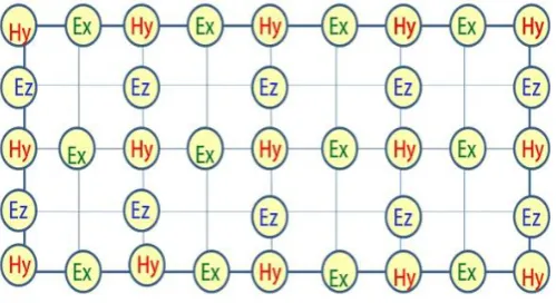
Figure 1. Electromagnetic field components on specific locations on FDTD grid system for TM polarized wave.
3. Design of GaAs-Based Solar Cell
In this section, we describe the solar cell design we have simulated using Optiwave software (OptiFDTD). This solar cell is composed of a semiconductor base with one-dimensional (1-D) nano-films/gratings on top. The incident light hits the nano-structures surface normally. Our study will focus on the geometrical properties of nano-structures made of GaAs, with the refractive index of 3.666 + i0.0612, on top of the same material, while the nano-structures’ height and pitch vary.
Furthermore, in this study, we investigate how covering the surface with nano-structures affects the solar cell performance, as varying the pitch size results in a change in the active area which is covered with nano-structures, e.g., 900 nm pitch size covers the entire surface. For consistency, the duty cycle, which defines the lateral width of the nano-structure in one pitch, is selected to be 100% throughout this study. Nonetheless, for triangular and trapezoidal geometries with 100% DC, the spacing between the ridges provides texture on the top surface; hence, the reflected light might strike the walls and be absorbed while this light on a flat surface is considered as loss. The specific geometries’ response will be discussed separately in the relevant sections, and R, A, and T of the solar cell devices will be calculated; thereby, depending on our simulation results, we will have an overview of the nano-structures’ suitable size for the experimental studies.
As shown in Figure 2, application of nano-structures helps to reduce the reflection while interacting with illuminated light. Figure 2b confirms even applying a thin film assists in more field absorption. We design rectangular, trapezoidal, and triangular nano-structures with heights ranging from 50 nm to 400 nm and the nano-structure pitches varying from 100 nm to 900 nm. Considering the wavelength of illumination in this study, 900 nm pitch would be excluded from the ZO diffraction grating; hence, the device performs differently for the nano-structures at 900 nm pitch compared with the shorter pitch sizes for all zero-order diffraction gratings.
A normal silicon PV cell has a thickness of around 200 µ m to 500 µ m. Considering the conventional methods, thinner films are not easy to fabricate and silicon has a low absorptivity factor which makes the usage of thicker films essential. Furthermore, thicker films provide good surface passivation and less surface recombination.
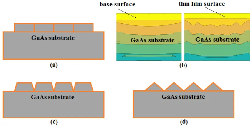
[image:4.595.174.424.154.290.2]However, we proposed a thin film based solar cell design with 1 µ m thickness of semiconductor material, i.e., GaAs. While the device might lose the conventional thick solar cell fabrication advantages, the flow of current and light trapping in the PV cell can be improved via application of periodic nano-structures; hence, less material is needed to absorb the solar flux which reduces the device size. Furthermore, nano-structures have the ability to make the electrons and holes less likely to interact on the PV cell surface. Oscillation of incident sunlight coupled with the free electrons on the surface of the nano-structures makes the e-h recombination less probable, and a high level of light trapping occurs in the GaAs thin film.
Figure 1. Electromagnetic field components on specific locations on FDTD grid system for TM polarized wave.
3. Design of GaAs-Based Solar Cell
In this section, we describe the solar cell design we have simulated using Optiwave software (OptiFDTD). This solar cell is composed of a semiconductor base with one-dimensional (1-D) nano-films/gratings on top. The incident light hits the nano-structures surface normally. Our study will focus on the geometrical properties of nano-structures made of GaAs, with the refractive index of 3.666 + i0.0612, on top of the same material, while the nano-structures’ height and pitch vary.
Furthermore, in this study, we investigate how covering the surface with nano-structures affects the solar cell performance, as varying the pitch size results in a change in the active area which is covered with nano-structures, e.g., 900 nm pitch size covers the entire surface. For consistency, the duty cycle, which defines the lateral width of the nano-structure in one pitch, is selected to be 100% throughout this study. Nonetheless, for triangular and trapezoidal geometries with 100% DC, the spacing between the ridges provides texture on the top surface; hence, the reflected light might strike the walls and be absorbed while this light on a flat surface is considered as loss. The specific geometries’ response will be discussed separately in the relevant sections, and R, A, and T of the solar cell devices will be calculated; thereby, depending on our simulation results, we will have an overview of the nano-structures’ suitable size for the experimental studies.
As shown in Figure 2, application of nano-structures helps to reduce the reflection while interacting with illuminated light. Figure2b confirms even applying a thin film assists in more field absorption. We design rectangular, trapezoidal, and triangular nano-structures with heights ranging from 50 nm to 400 nm and the nano-structure pitches varying from 100 nm to 900 nm. Considering the wavelength of illumination in this study, 900 nm pitch would be excluded from the ZO diffraction grating; hence, the device performs differently for the nano-structures at 900 nm pitch compared with the shorter pitch sizes for all zero-order diffraction gratings.
A normal silicon PV cell has a thickness of around 200µm to 500µm. Considering the conventional methods, thinner films are not easy to fabricate and silicon has a low absorptivity factor which makes the usage of thicker films essential. Furthermore, thicker films provide good surface passivation and less surface recombination.
on the PV cell surface. Oscillation of incident sunlight coupled with the free electrons on the surface of the nano-structures makes the e-h recombination less probable, and a high level of light trapping
[image:5.595.79.511.139.359.2]occurs in the GaAs thin film.Energies 2016, 9, 756 5 of 14
Figure 2. Schematic cross-section view of GaAs-based solar cell with (a) rectangular (thin film) (b) illustrates the electric field intensity plot for the solar cell without nanostructures (left) and a solar cell design with 50 nm thin film on top (right) (c) trapezoidal and (d) triangular nano-structure shapes to assist efficient light manipulation and trapping inside the device.
4. Optimization of Nano-Structured Solar Cell
In this section, we provide information about optimizing solar cell performance with application of different shaped nano-structures. For conventional solar cells, a substantial portion of light is expected to go through reflection losses [66]. Therefore, application of diffraction nano-structures would help as an optimization method.
Our design, apart from having ZO diffraction grating characteristics, provides a good property known as gradual change in refractive index which leads to a perfect anti-reflective (AR) medium. Hence, the nano-structures act like a homogeneous medium with an AR coating that allows to achieve lower reflection loss for a range of wavelengths and angles of incidence with respect to the incident light wavelength [67]. The first AR coating was experimentally presented on glass substrate by Fraunhofer in 1817 [68]. However, the concept of gradual transition in refractive index was first introduced by Lord Rayleigh in 1879 who mathematically reported the amount of reflection at the interface between tarnished glass and air [69].
On the other hand, the use of SW nano-structures in solar cell has also been validated by the insect eye design. The surface of an insect eye is covered with nano-structured film that absorbs most of the incident light with a minimal reflection which means there is almost no light diffraction. Due to this design, the refractive index between the air and the surface changes gradually, therefore, the light reflection decreases [70]. Inspired by insect eye design, the SW nano-structures are applied to the solar cells to increase the conversion efficiency and allow a larger portion of the electromagnetic wave to reach the embedded charge carrier zone [34].
For a fully AR coating layer, the light reflecting from substrate and AR coating layer have a destructive interference [71]. The minimum reflectance can be achieved when the refractive index equals the square root of the refractive indices of the two media [72]. The reflection loss of a SW nano-structure can be calculated easily using Fresnel's equation [73].
2
AR s
AR s
n
n
R
n
n
(1)where R is the reflectance, nARis the nano-structures/AR coating medium refractive index, and ns is
the substrate refractive index. For the current design, where both the diffraction nano-gratings and
Figure 2. Schematic cross-section view of GaAs-based solar cell with (a) rectangular (thin film) (b) illustrates the electric field intensity plot for the solar cell without nanostructures (left) and a solar cell design with 50 nm thin film on top (right) (c) trapezoidal and (d) triangular nano-structure shapes to assist efficient light manipulation and trapping inside the device.
4. Optimization of Nano-Structured Solar Cell
In this section, we provide information about optimizing solar cell performance with application of different shaped nano-structures. For conventional solar cells, a substantial portion of light is expected to go through reflection losses [66]. Therefore, application of diffraction nano-structures would help as an optimization method.
Our design, apart from having ZO diffraction grating characteristics, provides a good property known as gradual change in refractive index which leads to a perfect anti-reflective (AR) medium. Hence, the nano-structures act like a homogeneous medium with an AR coating that allows to achieve lower reflection loss for a range of wavelengths and angles of incidence with respect to the incident light wavelength [67]. The first AR coating was experimentally presented on glass substrate by Fraunhofer in 1817 [68]. However, the concept of gradual transition in refractive index was first introduced by Lord Rayleigh in 1879 who mathematically reported the amount of reflection at the interface between tarnished glass and air [69].
On the other hand, the use of SW nano-structures in solar cell has also been validated by the insect eye design. The surface of an insect eye is covered with nano-structured film that absorbs most of the incident light with a minimal reflection which means there is almost no light diffraction. Due to this design, the refractive index between the air and the surface changes gradually, therefore, the light reflection decreases [70]. Inspired by insect eye design, the SW nano-structures are applied to the solar cells to increase the conversion efficiency and allow a larger portion of the electromagnetic wave to reach the embedded charge carrier zone [34].
R=
nAR−ns nAR+ns
2
(1)
whereRis the reflectance,nARis the nano-structures/AR coating medium refractive index, and nsis the substrate refractive index. For the current design, where both the diffraction nano-gratings and substrate are made of the same material, the refractive index of the coating layer continuously changes fromnARtons[74].
Once the solar cell surface is illuminated, the photons hitting the top surface will either reflect from the top, or be absorbed by the semiconductor structure. Otherwise, they will be transmitted through the material [75]. However, only the absorbed photons are able to move an electron from the valence band to conduction band and generate power. Reflected and transmitted portions of sunlight are not desirable and are included in energy losses.
We made changes to the aspect ratios of the nano-structures which are responsible for the absorption and reflection of light in the PV cell. The aspect ratio is defined as a quantity to compare top and bottom bases of the nano-structures. For the aspect ratio of one, the SW nano-structure is rectangular; for the aspect ratio equalling zero, the SW nano-structure turns into triangular shape, and for any positive value of the aspect ratio between these two values, the SW nano-structure shape turns into trapezoidal.
4.1. Rectangular Shaped Nano-Structured Solar Cell
In this subsection, rectangular nano-gratings with 100% duty cycle and different thicknesses are studied. The mentioned design turns into uniform thin film on the top surface of the solar cell with different heights. Investigating this shape is necessary as under application of zero-order gratings and anti-reflective medium, it is assumed that the medium is a homogeneous slab. In the following, it is shown how a real homogeneous thin film affects the solar cell performance.
In Figure3, light reflection and absorption curves of the solar cells topped with rectangular nano-structures with 100% duty cycle are shown. Each curve illustrates the solar cell behavior with various nano-structure pitches and fixed nano-structure height. The curves consist of eight discrete data points having values associated with the maximum light reflection (Figure3a) and absorption (Figure3b) for eight different designs with related characteristics. The procedure is repeated for nano-structures with different heights in the range of 50 nm to 400 nm.Energies 2016, 9, 756 7 of 14
Figure 3. Light reflection (a) and absorption (b) values shown in percentage for solar cells with rectangular-shaped nano-structures.
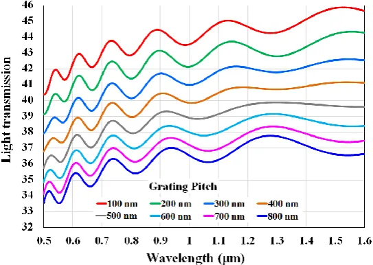
Figure 4. Light transmission values shown in percentage for solar cells with rectangular nano-structure on top. Each curve is associated with a specific pitch while the nano-gratings height is kept constant at 250 nm.
As the relation, T + R + A = 1 (total amount of light), is always satisfied for transmission, reflection, and absorption plots, the transmission plot behavior for different heights can be predicted given the results in Figure 3. Therefore, the least reflection and transmission occurs for the rectangular nano-structures with bigger pitches. Considering the results presented in Figures 3 and 4, the optimized size for nano-structures pitch is close to 800 nm, because a bigger part of the surface is covered with the thin film.
4.2. Trapezoidal Shaped Nano-Structured Solar Cell
[image:6.595.86.517.517.710.2]In Figure 5a,b, the light refection and absorption curves for trapezoidal nano-structures applied on the top surface of the solar cells are presented. Varying nano-structures’ height from 50 nm to 400 nm, the maximum reflection happens for 50 nm height and the least reflection occurs for 200 nm height data points. Comparing the results for thin films (Figure 3) with trapezoidal nano-structures (Figure 5) indicates that the thin film reflection behavior is smoother than trapezoidal ones; however, application of the trapezoidal nano-structures reduces the reflection minima for all heights. Furthermore, the transmission plot in Figure 5b also shows an increased absorption behavior for trapezoidal nano-gratings compared with the thin film design in Figure 3b. The plots in Figure 5
Energies2016,9, 756 7 of 14
The biggest and smallest nano-structure heights in Figure3a, i.e., 50 nm and 400 nm, have maximum reflection values regardless of the pitch size, and the light reflection associated with the nano-structures heights of 200 nm and 250 nm show the smallest reflection values, with 250 nm also having the maximum light absorption value. These results are satisfied for all pitch sizes. Therefore, 250 nm is the optimized height over the whole range of wavelengths for this design.
As shown in Figure3b, the absorption increases from 50 nm to 250 nm, and decreases afterwards, and these results are compatible with the absorption depth of GaAs.
To investigate how the thin film affects the solar cell performance, simulations are also performed for the solar cell without any nano-structure. The A, T, and R results for the 100 nm pitch and 50 nm height are almost the same as the solar cell without nano-structures. The electric field distribution of these structures are shown in Figure2b. However, for other pitches and heights, A, T, and R start to be different, as shown in Figures3and4.
Figure 3. Light reflection (a) and absorption (b) values shown in percentage for solar cells with rectangular-shaped nano-structures.
Figure 4. Light transmission values shown in percentage for solar cells with rectangular nano-structure on top. Each curve is associated with a specific pitch while the nano-gratings height is kept constant at 250 nm.
As the relation, T + R + A = 1 (total amount of light), is always satisfied for transmission, reflection, and absorption plots, the transmission plot behavior for different heights can be predicted given the results in Figure 3. Therefore, the least reflection and transmission occurs for the rectangular nano-structures with bigger pitches. Considering the results presented in Figures 3 and 4, the optimized size for nano-structures pitch is close to 800 nm, because a bigger part of the surface is covered with the thin film.
4.2. Trapezoidal Shaped Nano-Structured Solar Cell
In Figure 5a,b, the light refection and absorption curves for trapezoidal nano-structures applied on the top surface of the solar cells are presented. Varying nano-structures’ height from 50 nm to 400 nm, the maximum reflection happens for 50 nm height and the least reflection occurs for 200 nm height data points. Comparing the results for thin films (Figure 3) with trapezoidal nano-structures (Figure 5) indicates that the thin film reflection behavior is smoother than trapezoidal ones; however, application of the trapezoidal nano-structures reduces the reflection minima for all heights. Furthermore, the transmission plot in Figure 5b also shows an increased absorption behavior for trapezoidal nano-gratings compared with the thin film design in Figure 3b. The plots in Figure 5
Figure 4.Light transmission values shown in percentage for solar cells with rectangular nano-structure on top. Each curve is associated with a specific pitch while the nano-gratings height is kept constant at 250 nm.
Figure4shows the transmission curves for designs with different pitch sizes through the visible and near-infrared range wavelengths, while the thickness is kept constant at the value for which the maximum absorption and minimum reflection happens. The transmission decreases with increasing pitch size, and the undulating nature of the transmission curves originates from the light interference and reflections at the material interface.
As the relation, T + R + A = 1 (total amount of light), is always satisfied for transmission, reflection, and absorption plots, the transmission plot behavior for different heights can be predicted given the results in Figure3. Therefore, the least reflection and transmission occurs for the rectangular nano-structures with bigger pitches. Considering the results presented in Figures3and4, the optimized size for nano-structures pitch is close to 800 nm, because a bigger part of the surface is covered with the thin film.
4.2. Trapezoidal Shaped Nano-Structured Solar Cell
[image:7.595.162.434.265.458.2]of the trapezoidal nano-structures reduces the reflection minima for all heights. Furthermore, the transmission plot in Figure 5b also shows an increased absorption behavior for trapezoidal nano-gratings compared with the thin film design in Figure3b. The plots in Figure5represent one more data point, i.e., 900 nm pitch size for different heights. Considering the illuminating light wavelength, this pitch size does not satisfy zero-order gratings condition, the abrupt change at 900 nm pitch size for both plots confirms this fact.
Energies 2016, 9, 756 8 of 14
represent one more data point, i.e., 900 nm pitch size for different heights. Considering the illuminating light wavelength, this pitch size does not satisfy zero-order gratings condition, the abrupt change at 900 nm pitch size for both plots confirms this fact.
Figure 5. Light reflection (a) and absorption (b) curves shown in percentage for solar cells with trapezoidal nano-structures on the top surface of solar cell for different nano-structure pitches ranging from 100 nm to 900 nm.
4.3. Triangular Shaped Nano-Structured Solar Cell
In this subsection, we present results for triangular nano-structures applied on the top surface of the solar cell. This geometry will have sharp edges and, as an extreme case with aspect ratio of zero, it would be useful to study whether triangular nano-structures’ light reflection and absorption behavior is in favor of solar cell performance.
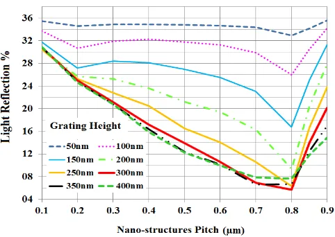
Maximum light reflection behavior of the solar cells with triangular nano-structures is shown in Figure 6 for different nano-structures’ heights. The minimum reflection occurs at 800 nm pitch for all different heights. Each curve is composed of a set of discrete values for the maximum reflection of fixed heights ranging from 50 nm to 400 nm. Therefore, based on the results shown in Figure 6, the nano-structure’s height having the least reflection in triangular case is 300 nm. To confirm that 800 nm pitch is the optimized size, it should also provide satisfactory light absorption behavior. The light absorption curves for the triangular nano-structures varying the pitch from 100 nm to 900 nm are shown in Figure 7. As can be seen, the maximum absorption occurs for 800 nm pitch along all different heights.
[image:8.595.81.517.183.341.2]Figure 6. Light reflection curves shown in percentage for solar cells with triangular nano-structures for different nano-structures’ pitch sizes. Each curve indicates the reflection behavior for a single height.
Figure 5. Light reflection (a) and absorption (b) curves shown in percentage for solar cells with trapezoidal nano-structures on the top surface of solar cell for different nano-structure pitches ranging from 100 nm to 900 nm.
4.3. Triangular Shaped Nano-Structured Solar Cell
In this subsection, we present results for triangular nano-structures applied on the top surface of the solar cell. This geometry will have sharp edges and, as an extreme case with aspect ratio of zero, it would be useful to study whether triangular nano-structures’ light reflection and absorption behavior is in favor of solar cell performance.
Maximum light reflection behavior of the solar cells with triangular nano-structures is shown in Figure6for different nano-structures’ heights. The minimum reflection occurs at 800 nm pitch for all different heights. Each curve is composed of a set of discrete values for the maximum reflection of fixed heights ranging from 50 nm to 400 nm. Therefore, based on the results shown in Figure6, the nano-structure’s height having the least reflection in triangular case is 300 nm. To confirm that 800 nm pitch is the optimized size, it should also provide satisfactory light absorption behavior. The light absorption curves for the triangular nano-structures varying the pitch from 100 nm to 900 nm are shown in Figure7. As can be seen, the maximum absorption occurs for 800 nm pitch along all different heights.
In Figure 8, we compare the results of nano-structures having one and zero aspect ratios rectangular (thin film) and triangular nano-structures, respectively. The horizontal axis in Figure8
Energies2016,9, 756 9 of 14 represent one more data point, i.e., 900 nm pitch size for different heights. Considering the illuminating light wavelength, this pitch size does not satisfy zero-order gratings condition, the abrupt change at 900 nm pitch size for both plots confirms this fact.
Figure 5. Light reflection (a) and absorption (b) curves shown in percentage for solar cells with trapezoidal nano-structures on the top surface of solar cell for different nano-structure pitches ranging from 100 nm to 900 nm.
4.3. Triangular Shaped Nano-Structured Solar Cell
In this subsection, we present results for triangular nano-structures applied on the top surface of the solar cell. This geometry will have sharp edges and, as an extreme case with aspect ratio of zero, it would be useful to study whether triangular nano-structures’ light reflection and absorption behavior is in favor of solar cell performance.
[image:9.595.178.419.86.257.2]Maximum light reflection behavior of the solar cells with triangular nano-structures is shown in Figure 6 for different nano-structures’ heights. The minimum reflection occurs at 800 nm pitch for all different heights. Each curve is composed of a set of discrete values for the maximum reflection of fixed heights ranging from 50 nm to 400 nm. Therefore, based on the results shown in Figure 6, the nano-structure’s height having the least reflection in triangular case is 300 nm. To confirm that 800 nm pitch is the optimized size, it should also provide satisfactory light absorption behavior. The light absorption curves for the triangular nano-structures varying the pitch from 100 nm to 900 nm are shown in Figure 7. As can be seen, the maximum absorption occurs for 800 nm pitch along all different heights.
Figure 6. Light reflection curves shown in percentage for solar cells with triangular nano-structures for different nano-structures’ pitch sizes. Each curve indicates the reflection behavior for a single height.
Figure 6.Light reflection curves shown in percentage for solar cells with triangular nano-structures for different nano-structures’ pitch sizes. Each curve indicates the reflection behavior for a single height.
Energies 2016, 9, 756 9 of 14
Figure 7. Light absorption curves in percentage for solar cells with triangular nano-structures for different nano-structures’ pitch sizes. Each curve indicates the absorption behavior for a single height.
In Figure 8, we compare the results of nano-structures having one and zero aspect ratios rectangular (thin film) and triangular nano-structures, respectively. The horizontal axis in Figure 8 shows the wavelength range for a fixed nano-structure height of 350 nm, and the light absorption behaviors of three different pitches are studied. Because the nano-structures’ heights are close to the optimized height of triangular structure, the maximum absorption occurs for triangular nano-structures. Furthermore, the light absorption for both rectangular and triangular nano-structures increases with size of the pitch. This means that a bigger portion of the surface is covered with nano-structures; hence, light interaction happens more effectively, having the best performance for the optimized pitch.
Figure 8. Light absorption curves in percentage for solar cells with triangular and rectangular nano-structures on the solar cell for different nano-structure pitches. The nano-nano-structures’ height is kept constant at 350 nm.
[image:9.595.186.408.306.478.2] [image:9.595.180.415.543.713.2]For each nano-structure geometry, the reflection is in close conjunction with absorption and transmission. A summary of the best combination of the mentioned parameters for rectangular, trapezoidal, and triangular shaped nano-structures is represented in Table 1.
Figure 7. Light absorption curves in percentage for solar cells with triangular nano-structures for different nano-structures’ pitch sizes. Each curve indicates the absorption behavior for a single height.
Energies 2016, 9, 756 9 of 14
Figure 7. Light absorption curves in percentage for solar cells with triangular nano-structures for different nano-structures’ pitch sizes. Each curve indicates the absorption behavior for a single height.
In Figure 8, we compare the results of nano-structures having one and zero aspect ratios rectangular (thin film) and triangular nano-structures, respectively. The horizontal axis in Figure 8 shows the wavelength range for a fixed nano-structure height of 350 nm, and the light absorption behaviors of three different pitches are studied. Because the nano-structures’ heights are close to the optimized height of triangular structure, the maximum absorption occurs for triangular nano-structures. Furthermore, the light absorption for both rectangular and triangular nano-structures increases with size of the pitch. This means that a bigger portion of the surface is covered with nano-structures; hence, light interaction happens more effectively, having the best performance for the optimized pitch.
Figure 8. Light absorption curves in percentage for solar cells with triangular and rectangular nano-structures on the solar cell for different nano-structure pitches. The nano-nano-structures’ height is kept constant at 350 nm.
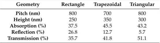
For each nano-structure geometry, the reflection is in close conjunction with absorption and transmission. A summary of the best combination of the mentioned parameters for rectangular, trapezoidal, and triangular shaped nano-structures is represented in Table 1.
For each nano-structure geometry, the reflection is in close conjunction with absorption and transmission. A summary of the best combination of the mentioned parameters for rectangular, trapezoidal, and triangular shaped nano-structures is represented in Table1.
Table 1.The optimized values in percentage for A, R, and T of three different nano-structure shapes are shown in Table1. The DC is 100%.
Geometry Rectangle Trapezoidal Triangular
Pitch (nm) 800 700 800
Height (nm) 250 350 300
Absorption (%) 37.5 45.5 43.2
Reflection (%) 26.8 12.7 5.7
Transmission (%) 35.7 41.8 51.1
5. Conclusions
In this paper, in order to optimize the solar cell design, diffraction nano-gratings have been employed on top of the solar cell from the same material to eliminate the unwanted reflection losses using the graded refractive index properties. Different subwavelength nano-structures, such as rectangular (the thin film), trapezoidal, and triangular shaped nano-gratings were designed on top of the GaAs-based solar cell and each geometry’s impact was examined under light illumination. As the nano-structures’ aspect ratios varied, the transmission, reflection and absorption performance of each design have been calculated, and the results were analyzed and compared. Based on our simulation plots, we introduced an optimized size for different nano-structured/diffraction grating shapes which represents better performance for the solar cells. The maximum absorption was calculated for trapezoidal nano-structures and the minimum reflection for triangular nano-structures. Therefore, it is confirmed that having slanted walls for the nano-structures on the top surface of solar cell would result in less reflection and better absorption as the surface area for incident light interaction increases. Development of GaAs-based solar cells revolutionary improves the photovoltaic market, and has a huge potential for application in various fields from household heating and generating electricity to telecommunications and transportation. This study would contribute to facilitating the fabrication process for construction of photovoltaic devices with better light absorption performance than conventional solar cells.
Acknowledgments: This research is supported by the Science Faculty, Department of Physics, University of Guilan, Iran; School of Engineering and Computer Science, Victoria University of Wellington, Wellington, New Zealand; and School of Mechanical and Electrical Engineering, Faculty of Health, Engineering, and Sciences, University of Southern Queensland, Toowoomba, Australia.
Author Contributions: F.F. Masouleh, N. Das, and S.M. Rozati conceived, designed, and performed the experiments, analyzed the data, and wrote the paper.
Conflicts of Interest:The authors declare no conflict of interest.
Abbreviations
The following abbreviations are used in this manuscript:
PV Photovoltaics
e-h Electron and hole PEC Photoelectrolysis cell GaAs gallium arsenide
SW Subwavelength
E Electric
ZO zero-order
H Magnetic
UV Ultraviolet
1-D One-dimensional
TM Transverse magnetic
nm Nanometer
µm Micrometer
AR Anti-reflective
DC Duty cycle
T Transmission
R Reflection
A Absorption
References
1. Holsten, H.H. Solar Energy Provides Electricity in Remote Areas. Available online: http://sciencenordic. com/solar-energy-provides-electricity-remote-areas (accessed on 8 August 2016).
2. Burger, B. Photovoltaics Report. Available online: https://www.ise.fraunhofer.de/de/downloads/pdf-files/aktuelles/photovoltaics-report-in-englischer-sprache.pdf (accessed on 8 August 2016).
3. Williams, R. Becquerel Photovoltaic Effect in Binary Compounds. J. Chem. Phys. 1960, 32, 1505–1514. [CrossRef]
4. Juodkazis, K.; Juodkazyt ˙e, J.; Jelmakas, E.; Kalinauskas, P.; Valsi ¯unas, I.; Mieˇcinskas, P.; Juodkazis, S. Photoelectrolysis of water: Solar Hydrogen—Achievements and Perspectives.Opt. Exp.2010,18, 147–160. [CrossRef] [PubMed]
5. Liu, J.; Liu, Y.; Liu, N.; Han, Y.; Zhang, X.; Huang, H.; Lifshitz, Y.; Lee, S.; Zhong, J.; Kang, Z. Metal-free efficient photocatalyst for stable visible water splitting via a two-electron pathway.Science2015,347, 970–974. [CrossRef] [PubMed]
6. Wahab, N.B.A.; Khan, S.A. Optimum doping for n+p silicon solar cell and the J-V characteristic. In Proceedings of the 2012 International Conference on Enabling Science and Nanotechnology (ESciNano), Johor Bahru, Malaysia, 5–7 January 2012.
7. Yang, D.; Yu, X.; Li, X.; Wang, P.; Wang, L. Germanium-doped crystal silicon for solar cells. In Proceedings of the 2010 10th IEEE International Conference on Solid-State and Integrated Circuit Technology (ICSICT), Shanghai, China, 1–4 November 2010.
8. Chasteen, S.; Chaddha, R. How Do Solar Panels Work? Available online: http://www.livescience.com/ 41995-how-do-solar-panels-work.html (accessed on 8 August 2016).
9. Wang, U. Clearing the Way for Cheap, Flexible Solar Panels. Available online: https:// www.technologyreview.com/s/421190/clearing-the-way-for-cheap-flexible-solar-panels/ (accessed on 1 June 2016).
10. Badawy, W.A. A review on solar cells from Si-single crystals to porous materials and quantum dots.J. Adv. Res. 2015,6, 123–132. [CrossRef] [PubMed]
11. Lungenschmied, C.; Dennler, G.; Neugebauer, H.; Sariciftci, S.N.; Glatthaar, M.; Meyer, T.; Meyer, A. Flexible, long-lived, large-area, organic solar cells.Sol. Energy Mater. Sol. Cells2007,91, 379–384. [CrossRef]
12. Broggi, A.; Tomasi, I.; Bianchi, L.; Marrocchi, A.; Vaccaro, L. Small Molecular Aryl Acetylenes: Chemically Tailoring High-Efficiency Organic Semiconductors for Solar Cells and Field-Effect Transistors. Chem. Plus. Chem.2014,79, 486–507. [CrossRef]
13. Cheng, Y.J.; Yang, S.H.; Hsu, C.S. Synthesis of conjugated polymers for organic solar cell applications. Chem. Rev.2009,109, 5868–5923. [CrossRef] [PubMed]
14. Sauvage, F.; Chen, D.; Comte, P.; Huang, L.H.F.; Cheng, Y.; Caruso, R.A.; Graetzel, M. Dye-Sensitized Solar Cells Employing a Single Film of Mesoporous TiO2Beads Achieve Power Conversion Efficiencies Over 10%. ACS Nano2010,4, 4420–4425. [CrossRef] [PubMed]
15. Huang, H.; Chen, H.; Long, J.; Wang, G.; Tan, S. Novel D–A–π–A organic dyes based on 3-dimensional triarylamine and benzothiadiazole derivatives for high-performance dye-sensitized.J. Power Sources2016, 326, 438–446. [CrossRef]
16. Hu, Y.; Robertson, N. Atypical organic dyes used as sensitizers for efficient dye-sensitized solar cells. Front. Optoelectron.2016,9, 38–43. [CrossRef]
17. Law, M.; Greene, L.E.; Johnson, J.C.; Saykally, R.; Yang, A.P. Nanowire dye-sensitized solar cells.Nat. Mater. 2005,4, 455–459. [CrossRef] [PubMed]
19. Hu, L.; Chen, G. Analysis of Optical Absorption in Silicon Nanowire Arrays for Photovoltaic Applications. Nano Lett.2007,7, 3249–3252. [CrossRef] [PubMed]
20. Nozik, A.J. Nanoscience and Nanostructures for Photovoltaics and Solar Fuels.Nano Lett.2010,10, 2735–2741. [CrossRef] [PubMed]
21. Phelps, M. The Best States for Solar Power. 2009. Available online: http://www.motherearthnews.com/ renewable-energy/solar-power/solar-incentives-solar-power-resources.aspx (accessed on 8 August 2016). 22. Kemery, B.P. Optimal PV orientation and geographic dispersion: A study of 10 Canadian cities and 16 Ontario locations. In Proceedings of the Canadian Conference on Building Simulation, Halifax, NS, Canada, 1–4 May 2012.
23. Hodgkins, K. Researchers develop cool way to improve solar cell efficiency. 2015. Available online: http: //www.digitaltrends.com/cool-tech/stanford-solar-panel-heat/ (accessed on 8 August 2016).
24. Yamaguchi, M.; Luque, A. High efficiency and high concentration in photovoltaics. IEEE Trans. Electron. Devices1999,46, 41–46. [CrossRef]
25. Fan, Z.; Lin, Q. Reducing reflection losses in solar cells. Available online: http://spie.org/newsroom/5343-reducing-reflection-losses-in-solar-cells (accessed on 8 August 2016).
26. Adams, P. Glass Coating Makes Solar Panels More Efficient. 2015; Available online: http://energy.gov/ articles/glass-coating-makes-solar-panels-more-efficient (accessed on 8 August 2016).
27. Ebbesen, T.W.; Lezec, H.J.; Ghaemi, H.F.; Thio, T. Extraordinary optical transmission through sub-wavelength hole arrays.Nature1998,391, 667–668. [CrossRef]
28. Søndergaard, T.; Bozhevolnyi, S.I.; Novikov, S.M.; Beermann, J. Extraordinary Optical Transmission Enhanced by Nanofocusing.Nano Lett.2010,10, 3123–3128. [CrossRef] [PubMed]
29. Dühring, M.B.; Sigmund, O. Optimization of extraordinary optical absorption in plasmonic and dielectric structures.J. Opt. Soc. Am. B2013,30, 1154–1160. [CrossRef]
30. Tsakalakos, L.; Balch, J.; Fronheiser, J.; Korevaar, B.A.; Sulima, O.; Rand, J. Silicon nanowire solar cells. Appl. Phys. Lett.2007,91. [CrossRef]
31. Zhu, J.; Yu, Z.; Burkhard, G.F.; Hsu, C.M.; Connor, S.T.; Xu, Y.; Wang, Q.; McGehee, M.; Fan, S.H.; Cui, Y. Optical Absorption Enhancement in Amorphous Silicon Nanowire and Nanocone Arrays.Nano Lett.2009,9, 279–282. [CrossRef] [PubMed]
32. Cao, L.; Fan, P.; Vasudev, A.P.; White, J.S.; Yu, Z.; Cai, W. Semiconductor Nanowire Optical Antenna Solar Absorbers.Nano Lett.2010,10, 439–445. [CrossRef] [PubMed]
33. Dühring, M.B.; Mortensen, N.A.; Sigmund, O. Plasmonic versus dielectric enhancement in thin-film solar cells.Appl. Phys. Lett.2012,100. [CrossRef]
34. Moushumy, N.; Das, N.; Alameh, K.; Lee, Y. Design and development of silver nanoparticles to reduce the reflection loss of solar cells. In Proceedings of the 8th International Conference on High-capacity Optical Networks and Emerging Technologies, Riyadh, Saudi Arabia, 19–21 December 2011.
35. Das, N.; Charoenpitaks, K.; Islam, S. Analysis of incident light angles on nano-grating structure for minimizing reflection losses in GaAs solar cells. In Proceedings of the Power Engineering Conference (AUPEC), Hobart, Australia, 29 September–3 October 2013.
36. Das, N.; Abu-Saida, A.; Islam, S. High efficiency plasmonics-based solar cells for smarter electricity grids. In Proceedings of the 2011 IEEE PES on Innovative Smart Grid Technologies Asia (ISGT), Perth, Australia, 13–16 November 2011.
37. Das, N.; Masouleh, F.F.; Mashayekhi, H.R. Light Absorption and Reflection in Nanostructured GaAs Metal–Semiconductor–Metal Photodetectors.IEEE Trans. Nanotechnol.2014,13, 982–989. [CrossRef] 38. Masouleh, F.F.; Das, N.; Mashayekhi, H.R. Assessment of amplifying effects of ridges spacing and height on
nano-structured MSM photo-detectors.Opt. Quantum Electron.2015,47, 193–201. [CrossRef]
39. Alenezi, M.R.; Henley, S.J.; Emerson, N.G.; Silva, S.R.P. From 1D and 2D ZnO nanostructures to 3D hierarchical structures with enhanced gas sensing properties. Nanoscale2014, 6, 235–247. [CrossRef] [PubMed]
40. Xia, Y.; Yang, P.; Sun, Y.; Wu, Y.; Mayers, B.; Gates, B.; Yin, Y.; Kim, F.; Yan, H. One-Dimensional Nanostructures: Synthesis, Characterization, and Applications.Adv. Mater.2003,15, 353–389. [CrossRef] 41. Masouleh, F.F.; Das, N.; Rozati, S.M. Optimal subwavelength design for efficient light trapping in central slit
42. Beard, M.C.; Luther, J.M.; Nozik, A.J. The promise and challenge of nanostructured solar cells. Nat. Nanotechnol.2014,9, 951–954. [CrossRef] [PubMed]
43. Natale, C.D. Sensors and Microsystems. In Proceedings of the 8th Italian Conference, Trento, Italy, 12–14 February 2003.
44. Lei, K. Materials and Fabrication Techniques for Nano- and Microfluidic Devices. InMicrofluidics in Detection Science: Lab-on-a-Chip Technologies; Labeed, F.H., Fatoyinbo, H.O., Eds.; Royal Society of Chemistry: London, UK, 2014; pp. 1–28. [CrossRef]
45. Applications-GaAs Solar Cells. Available online: http://photonetc.com/gaas (accessed on 8 August 2016). 46. Hayes, G.J.; Clemens, B.M. Laser liftoff of gallium arsenide thin films.MRS Commun.2015,5, 1–5. [CrossRef] 47. The Future of Solar Energy: An interdisciplinary MIT study. Available online: https://cleanenergysolutions.
org/resources/future-solar-energy-interdisciplinary-mit-study (accessed on 8 August 2016).
48. Miles, R. Photovoltaic solar cells: Choice of materials and production methods.Vacuum2006,80, 1090–1097. [CrossRef]
49. Why Gallium Arsenide? Alta Devices, 2015. Available online: http://www.altadevices.com/solar-cells/ why-gallium-arsenide/ (accessed on 8 August 2016).
50. Kayes, B.M.; Nie, H.; Twist, R.; Spruytte, S.G.; Reinhardt, F.; Kizilyalli, I.C.; Higashi, G.S. 27.6% conversion efficiency, a new record for single-junction solar cells under 1 sun illumination. In Proceedings of the IEEE Photovoltaic Specialists Conference (PVSC), Seattle, WA, USA, 19–24 June 2011.
51. Grandidier, J.; Watson, T.J.; Callahan, D.M.; Munday, J.N.; Atwater, H.A. Gallium Arsenide Solar Cell Absorption Enhancement Using Whispering Gallery Modes of Dielectric Nanospheres.IEEE J. Photovolt. 2012,2, 123–128. [CrossRef]
52. Green, M.A.; Emery, K.; Hishikawa, Y.; Warta, W.; Dunlop, E.D. Solar cell efficiency tables (Version 45). Prog. Photovolt.2015,23, 1–9. [CrossRef]
53. Wang, X.; Khan, M.R.; Gray, J.L.; Alam, M.A. Design of GaAs Solar Cells Operating Close to the Shockley–Queisser Limit.IEEE J. Photovolt.2013,3, 737–744. [CrossRef]
54. Sheridan, J.; Coutsomitros, C.T.; Lucia, A.Zero Order Gratings: Homogenisation and the Effective Index Model; European Commission: Brussels, Belgium, 1996.
55. Gorb, S.N.Functional Surfaces in Biology: Little Structures with Big Effects; Springer: New York, NY, USA, 2009. 56. Raut, H.K.; Ganesh, V.A.; Nair, A.S.; Ramakrishna, S. Anti-reflective coatings: A critical, in-depth review.
Energy Environ. Sci.2011,4, 3779–3804. [CrossRef]
57. Stork, W.; Streibl, N.; Haidner, H.; Kipfer, P. Artificial distributed-index media fabricated by zero-order gratings.Opt. Lett.1991,16, 1921–1923. [CrossRef] [PubMed]
58. Lalanne, P.; Hutley, M. Artificial Media Optical Properties-Subwavelength Scale. Encycl.Opt. Eng.2003,1, 62–71.
59. Honsberg, C.B.; Barnett, A.M.; Kirkpatrick, D. Nanostructured Solar Cells for High Efficiency Photovoltaics. In Proceedings of the 2006 IEEE 4th World Conference on Photovoltaic Energy Conference, Waikoloa, HI, USA, 7–12 May 2006.
60. Akatemia, S. Nanostructures Improve the Efficiency of Solar Cells. 2013. Available online: https://www. sciencedaily.com/releases/2013/04/130425091358.htm (accessed on 8 August 2016).
61. Jin, J.M.Theory and Computation of Electromagnetic Fields; John Wiley & Sons Ltd: Hoboken, NJ, USA, 2010. 62. Yu, W.Electromagnetic Simulation Techniques Based on the FDTD Method; John Wiley & Sons Ltd: Hoboken, NJ,
USA, 2009.
63. Finite Difference Time Domain Photonics Simulation Software, OptiFDTD Technical background and Tutorials. Version 8. Available online: http://www.optiwave.com/products/fdtd_overview.html (accessed on 8 August 2016).
64. Ellingson, R.; Nozik, A.; Beard, M.; Johnson, J.; Murphy, J.; Knutsen, K.; Gerth, K.; Luther, J.; Hanna, M.; Micic, O.; et al. Nanocrystals generating >1 electron per photon may lead to increased solar cell efficiency. Nano Lett.2005,5, 865–871. [CrossRef] [PubMed]
65. Jha, A.R.Solar Cell Technology and Applications; CRC Press, Taylor and Francis Group: Boca Raton, FL, USA, 2009.
67. Song, Y.M.; Lee, Y.T. Simulation of antireflective subwavelength grating structure for optical device applications. In Proceedings of the 9th International Conference on Numerical Simulations of Optoelectronic Devices (NUSOD), Gwangju, Korea, 14–17 September 2009.
68. von Fraunhofer, J.Joseph von Fraunhofer’s Gesammelte Schriften—Primary Source Edition; Nabu Press: Munich, Germany, 1888.
69. Rayleigh, L. On Reflection of Vibrations at the Confines of two Media between which the Transition is Gradual.Proc. Lond. Math. Soc.1879,1, 48–51. [CrossRef]
70. Thelen, A.Design of Optical Interference Coatings; McGraw-Hill Optical and Electro-Optical Engineering Series; McGraw-Hill: New York, NY, USA, 1989.
71. Prevo, B.G.; Hwang, Y.; Velev, O.D. Convective Assembly of Antireflective Silica Coatings with Controlled Thickness and Refractive Index.Chem. Mater.2005,17, 3642–3651. [CrossRef]
72. Schmid, J.H.; Cheben, P.; Janz, S.; Lapointe, J.; Post, E.; Delage, A.; Densmore, A.; Lamontagne, B.; Waldron, P.; Xu, D.X. Subwavelength grating structures in planar waveguide facets for modified reflectivity. Adv. Opt. Technol.2008. [CrossRef]
73. Gupta, S.C.Optoelectronic Device and Systems; PHI Learning: Delhi, India, 2014.
74. Antireflection Coatings Made by a Sol–Gel Process. Available online: http://www.rug.nl/research/portal/ files/2972404/c4.pdf (accessed on 8 August 2016).
75. Albregtsen, F. Reflection, Refraction, Diffraction, and Scattering. Available online: https://www.uio.no/ studier/emner/matnat/ifi/INF-GEO4310/h09/undervisningsmateriale/imaging-kap2.pdf (accessed on 8 August 2016).