J. Phys. D: Appl. Phys.37(2004) R75–R85 PII: S0022-3727(04)35483-5
TOPICAL REVIEW
Vertical-external-cavity semiconductor
lasers
A C Tropper
1, H D Foreman
1, A Garnache
2, K G Wilcox
1and
S H Hoogland
11School of Physics and Astronomy, University of Southampton, Southampton SO17 1BJ, UK 2CEM2 Universit´e Montpellier 2, 34095 Montpellier Cedex 05, France
Received 14 January 2004 Published 14 April 2004
Online atstacks.iop.org/JPhysD/37/R75 DOI: 10.1088/0022-3727/37/9/R01
Abstract
Surface-emitting semiconductor lasers can make use of external cavities and optical pumping techniques to achieve a combination of high
continuous-wave output power and near-diffraction-limited beam quality that is not matched by any other type of semiconductor source. The ready access to the laser mode that the external cavity provides has been exploited for applications such as intra-cavity frequency doubling and passive mode-locking. The purpose of this Topical Review is to outline the
operating principles of these versatile lasers and summarize the capabilities of devices that have been demonstrated so far. Particular attention is paid to the generation of near-transform-limited sub-picosecond pulses in passively mode-locked surface-emitting lasers, which are potentially of interest as compact sources of ultrashort pulses at high average power that can be operated readily at repetition rates of many gigahertz.
1. Introduction
The growing current interest in vertical-external-cavity surface-emitting lasers (VECSELs) is at first sight paradoxical since these lasers incorporate precisely the feature that conventional semiconductor lasers most prize the lack of: a bulky external cavity that requires alignment. They are frequently, moreover, optically pumped, exploiting the diode beam coupling technologies that have been developed for diode-pumped solid state lasers. On further investigation, however, it becomes apparent that this family of devices offers a distinctive combination of properties not easily matched by any other type of laser source. The aim of this review is to provide a concise introduction to the distinctive characteristics of the VECSEL and to outline the work that has been done to date.
A VECSEL resembles a diode-pumped solid state disc laser in construction [1], except that the dielectric laser disc is replaced by a surface-emitting semiconductor active mirror structure, which may be optically or electrically pumped. The mirror structure contains a distributed Bragg reflector (DBR) over which is grown an active region containing quantum wells. An external laser cavity enforces output in a low-divergence,
circular, near-diffraction-limited beam of high quality. Disc lasers are power-scalable because the active region is cooled by a one-dimensional heat flow, and the associated thermal gradient is along the axis of the optical cavity, minimizing the problems associated with thermal lensing and depolarization. The power-scaling potential of a semiconductor disc laser with a large active area was first highlighted by Leet al[2], who reported 500 W peak power in pulsed operation from a disc of bulk n-type GaAs 135µm thick. Since the area of the spatial mode on the surface of the gain structure can be large, the power that can be extracted in a fundamental spatial mode before the optical damage threshold is reached exceeds greatly that which can be obtained from a conventional diode laser.
barrier material is typically∼0.8µm−1, so that pump radiation
can be absorbed efficiently on a single or double pass of even a very thin active region. Thus the mirror arrays, which in dielectric disc lasers back-reflect the pump beam to make multiple passes, are unnecessary in VECSELs.
The carriers that are created by optical pumping in the barriers are trapped subsequently in the quantum wells. The gain bandwidth, differential gain, peak gain wavelength, and quantum efficiency depend sensitively on carrier concentration and temperature. The active mirror is therefore affected by the pump power level, pump spot-size, and thermal coupling to the heat sink more strongly than is the gain medium of a dielectric disc laser. The gain bandwidth of the laser transition is typically some tens of nanometres—of interest for spectroscopic applications and also for the generation of ultrashort pulses.
The second section of this review outlines the physical principles that govern the design of these devices, and reviews recent progress in the development of VECSELs operating at high average power. The third section reviews progress in the fabrication of VECSELs using various quantum well systems operating at different wavelengths. The development of practical blue sources based on frequency-doubled VECSELs is also discussed. The fourth section is devoted to mode-locked operation and the generation of ultrashort pulses at high repetition rates, including the demonstration of soliton sub-picosecond pulses. In conclusion, some of the more interesting potential developments of the field are discussed.
2. Device principles
2.1. Gain structure and external cavity
The essential features of an epitaxially grown semiconductor structure that might form the gain element of an InGaAs/GaAs-based VECSEL appear in figure 1(a), which shows the variation of the bandgap with vertical position in the epilayer. The GaAs-based structure resembles a VCSEL, which is modified by replacing one of the DBR mirrors by a transparent window layer. The active region consists of a periodic array of
1.0 1.5 2.0 2.5
(b)
(a) Capping layer
Window layer
Substrate DBR
Active region
B
andgap [eV]
z
|E
| 2
B
a
ndgap
[image:2.595.62.290.551.705.2]...
Figure 1.(a) Bandgap as a function of vertical position,z, within
the layer for a 1-µm VECSEL design containing six InGaAs
quantum wells spaced atλ/2 intervals within a GaAs active region
of overall thickness 7λ/2, between an AlAs window layer and a
27-period AlAs/GaAs Bragg reflector. (b) Expanded sketch of the
active region showing the variation of|E|2withz.
InGaAs quantum wells, spaced at half-wavelength intervals by GaAs barrier/spacer layers. In most implementations to date the wells are pumped optically, using incident pump radiation from a diode or other laser source at a wavelength that is absorbed by interband transitions within the barriers. The structure is therefore undoped, and there is no need for the DBR to incorporate composition grading schemes, which impair optical efficiency in order to reduce electrical impedance.
A striking difference between the VECSEL active mirror and its solid state laser counterpart is the strong coupling between quantum-confined carriers and light in the semiconductor structure. The optical dipole transition is allowed, unlike the first-order-forbidden optical transitions of impurity ions in dielectrics, leading to a differential gain coefficient that is more than three orders of magnitude greater than the typical value of the emission cross-section of a dielectric laser transition. The quantum well can therefore exhibit an effective exponential gain coefficient as high as ∼6000 cm−1. A small number of wells, thickness∼10 nm,
therefore suffices to develop a gain of several per cent in a surface-emitting geometry. The gain is thus localized spatially within layers that are thin compared with the wavelength of the light in the medium. The effective gain is proportional to the longitudinal confinement factor,γ, given by
γ =
i
|E(zi)|2,
where E(zi) is the E-field amplitude of the standing wave
within the active region at the position, zi, of the ith
quantum well. Figure 1(b) shows the spatial intensity distribution of this standing wave at the design wavelength.
The longitudinal confinement factor is analogous to the modal overlap factor of an edge-emitting laser; however, in a surface-emitting laser the longitudinal confinement factor introduces a strong spectral filtering effect, which significantly controls the performance of the device. The spectral dependence of the longitudinal confinement factor is controlled by the optical sub-cavity formed by the DBR and the air surface. A sharp resonance of this sub-cavity at the operating wavelength of a structure in which the quantum wells are positioned accurately at field antinodes can enhance greatly the longitudinal confinement factor and hence the effective gain of the device: the cost is the narrowness of the associated filter peak. As the active region is heated by pumping, the optical layer thicknesses tune to longer wavelengths at a rate of ∼0.1 nm K−1, and the resonance peak walks away from
the operating wavelength, causing the effective gain of the device to diminish.
The gain of a quantum well laser is intrinsically temperature-dependent; the peak of the gain profile shifts to longer wavelengths with increasing temperature at a rate of roughly 0.3 nm K−1. The peak gain coefficient,
moreover, declines rapidly with increasing temperature: the characteristic temperature,T0, is an empirical parameter used
heat sink
SESAM
OC
surface-emitting
MQW structure
pump laser
[image:3.595.70.273.82.269.2]laser output
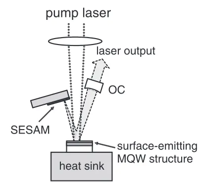
Figure 2.Schematic diagram of a VECSELV-cavity arrangement,
with a surface-emitting multiquantum well structure pumped at normal incidence, and a spherical output coupler mirror (OC). The third cavity mirror here is a SESAM, with which the VECSEL may be mode-locked passively as described in section 4.
also rises, and eventually thermal runaway switches off the laser. These effects are familiar in edge-emitting diodes but contrast unfavourably with the relatively temperature-insensitive gain observed in impurity-doped dielectric laser media. The problem of thermal runaway may be exacerbated in surface-emitting lasers by the spectral filtering effect of the longitudinal confinement factor. Section 2.2 describes some approaches to the design of the active region that alleviate this problem.
For high power operation, the VECSEL may use a simple two-mirror cavity formed by the active mirror gain structure together with a spherical output coupler. Many VECSEL applications exploit the ready access to the cavity mode and incorporate intra-cavity elements such as semiconductor saturable absorber mirrors (SESAMs) or nonlinear crystals. For these applications a more complexV-, Z-, orW-shaped cavity may be designed to set the mode spot-size at required values on each active element of the cavity. A simple example is shown in figure 2, which depicts aV-shaped laser cavity with the gain structure mirror placed at the fold and pumped at normal incidence. A key design requirement is that the spherical output coupler mirror defines a TEM00cavity mode
with a spot-size on the gain structure matched to that of the incident pump radiation. The cavity depicted here was designed with a tight mode focus on one end mirror, where it was intended to insert a saturable absorber mirror for passive mode-locking, as discussed in section 4.
2.2. High power operation
Kuznetsov and his co-workers made the first demonstration of a VECSEL that was diode-pumped and operated at high power with high beam quality. Their device used a GaAs-based gain wafer, in which the active region contained 13 In0.16Ga0.84As/GaAs quantum wells designed for operation
near 980 nm. A 3-W 808-nm broad-stripe diode pumped the device, which could be operated with a 4% output coupler. These authors reported a maximum output power of 0.69 W
in a predominantly TEM11 beam; they were also able to
demonstrate TEM00 operation with 0.37 W of output power
coupled into a single-mode optical fibre [3].
Holm et al [4] described a similar laser structure, but grown this time in lattice-matched AlGaAs/GaAs material, with a shorter operating wavelength of 870 nm. This quantum well system exhibits both lower differential gain and lower
T0relative to the strained InGaAs/GaAs system; nevertheless,
these authors were able to demonstrate an output of 0.15 W, with 850 mW of incident pump radiation supplied by a pair of polarization-coupled 670-nm pump diodes and with the gain structure thermoelectrically cooled to∼0˚C.
Both these early reports describe devices in which the active region forms a resonant sub-cavity, enhancing the effective gain at the expense of a relatively narrow filter function, with the disadvantages discussed in section 2.1. Careful design of the active region can achieve a broad spectral filter characteristic, with the advantage for thermal management that it is relatively insensitive to temperature excursions. Garnache et al [5] analysed the filter characteristics of several generic types of VECSEL gain structure and showed that if a short sub-cavity is made anti-resonant at the operating wavelength, with a narrow-band anti-reflection structure at the air surface, then not only is the spectral filter nearly flat over a bandwidth of order 10 nm but the effective gain bandwidth of the quantum wells can be larger than the intrinsic width also. Although this type of design has no resonant enhancement of the effective gain, it can nevertheless exhibit a low laser threshold. Holmet al
[6] have also reported an early example of an an anti-resonant design, used to accomplish single-frequency second harmonic generation in a VECSEL.
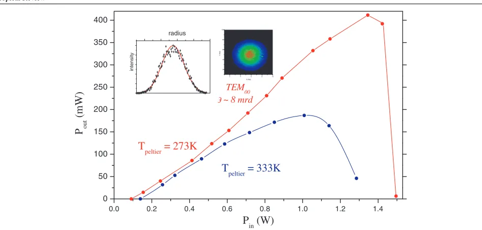
The Garnache design was implemented in an MBE-grown InGaAs/GaAs VECSEL, which exhibited the power output characteristics shown in figure 3. Unlike the Kuznetsov device, this laser used no post-growth processing of any kind to reduce thermal impedance: the back surface of the intact substrate of the gain structure was made to contact a Peltier cooler using thermally conductive paste. The VECSEL was pumped with up to 1.5 W of 830-nm radiation from a fibre-coupled diode, imaged onto a 90-µm-diameter spot on the surface of the gain structure. Figure 3 shows the output power of this laser as a function of incident pump power for two temperature settings of the Peltier cooler. With the device running above ambient temperature, at a Peltier setting of 60˚C, the output power rolls over slowly and smoothly, passing through a maximum of
>190 mW. The broad rollover characteristic indicates a device limited only by the intrinsic temperature dependence of the quantum well gain and not by thermal tuning of the longitudinal confinement factor. The laser was almost completely turned off for an incident pump power of 1.3 W, at which point the temperature of the active region reached an estimated 130˚C. With the Peltier cooler set to 0˚C, the laser reached a maximum output power of>400 mW, corresponding to an overall power conversion efficiency of∼30%, enhanced by careful design of the DBR to back-reflect the unabsorbed pump light through the wells. The VECSEL operated in a TEM00mode up to the
0.0 0.2 0.4 0.6 0.8 1.0 1.2 1.4
0 50 100 150 200 250 300 350 400
T
peltier= 333K
T
peltier= 273K
TEM00
θ ~ 8 mrd
2 4 6 8 10
2 4 6 8 10
X Axis
Y Ax
is
radius
intensity
P
out(mW
)
[image:4.595.63.537.76.302.2]P
in(W)
Figure 3.Output power from a 1-µm VECSEL as a function of incident pump power for two temperature settings of the Peltier cooler on
which the unprocessed InGaAs/GaAs gain structure is mounted. The spatial profile of the TEM00mode is shown inset.
(This figure is in colour only in the electronic version)
further power scaling, it is essential to process the wafer to reduce the thermal impedance between the hot active region and the heat sink. In the original work by Kuznetsovet al, the gain structure was grown ‘upside-down’, that is with the quantum wells adjacent to the GaAs substrate, and the 30-layer DBR grown over the quantum wells. The MOVPE-grown epilayer was bonded to a diamond heat sink, and the substrate of the wafer then removed by etching, exposing an AlGaAs window that formed the active surface of the device after being provided with an appropriate anti-reflection coating [7]. Heat was thus extracted through the DBR, which was composed of alternating λ/4 layers of AlAs/AlGaAs. The thermal conductivity of the ternary alloy can be as low as 11 W m−1K−1
for compositions close to Al0.5Ga0.5As. A similar approach has
enabled H¨aringet al[8] to demonstrate 2.2 W in cw operation in a near-diffraction-limited beam.
An effective technique that extracts heat directly from the active region, rather than through the DBR, was introduced by Alford et al[9], who put an uncoated sapphire window incontact with the front surface of a VECSEL gain element, where it acted as a heat-spreading plate. These authors were able to report a maximum output power of 1.6 W in cw operation without any substrate removal. Their InGaAs/GaAs VECSEL operated at wavelengths around 985 nm, pumped by a fibre-bundle-coupled 814-nm diode bar. They observed the onset of thermal runaway at an incident pump power of 9 W. With the sapphire window to disperse heat, they were able to use a larger pumped area than had hitherto been reported, of diameter 500µm.
The heat spreading plate technique has been applied by Hastieet alto a GaAs/AlGaAs VECSEL operating at 850 nm. In place of sapphire, these authors use SiC for the heat-spreading plate, with a thermal conductivity larger by more than an order of magnitude than that of sapphire [10]. They observed a maximum output power of 0.5 W in a circular TEM00beam, with a slope efficiency of∼32% with respect
to pump power transmitted through the surface of the plate. In a further refinement of the concept, these authors have demonstrated microchip VECSELs [11], in which the cavity is formed by the VECSEL semiconductor DBR, and a dielectric mirror coated onto the surface of the sapphire plate. An 850-nm GaAs/AlGaAs microchip VECSEL was pumped at normal incidence by a krypton-ion laser supplying up to 2.5 W at 647 nm: the high beam quality of the gas laser allowed the pump to be focused tightly to a 25-µm spot. This device emitted>350 mW for an incident pump power of 2.2 W, with output in a TEM00mode. These authors also report a 980-nm
InGaAs/GaAs VECSEL emitting 1.7 W when pumped with ∼8 W of 810-nm radiation from a fibre-coupled diode, with the microchip maintained at a temperature of 20˚C. On cooling the microchip to 0˚C, the output power increased to 2.5 W. The output beam at these power levels was circularly symmetric but spatially multimode.
The power-scaling potential of VECSELs has been demonstrated decisively by some recent results. Lutgenet al
with a two-mirror cavity that operated multitransverse mode, withM2values typically around three. They also report the high power blue operation at 488 and 460 nm described in section 3.2.
High power operation of VECSELs using electrical pumping has been developed by a group at Novalux, who describe their distinctive device as a NECSEL. McInerneyet al
[15] report an electrically pumped VECSEL emitting at 980 nm that can deliver 1 W cw in a multimode beam, and 0.5 W in a single transverse mode, with 90% coupling efficiency into a single-mode optical fibre. The laser uses a linear three-mirror coupled cavity design, with strained InGaAs quantum wells in an active region enclosed between a highly reflecting p-doped GaAs/AlGaAs DBR and a partially reflecting n-doped DBR with a reflectivity in the range 70–80%. Light transmitted through the n-DBR traverses the substrate, which has low optical loss at the lasing wavelength. The cavity may be completed by a dielectric coating on the plane surface of the substrate, in which case the device can emit up to ∼10 mW in a TEM00 beam from an emitting aperture of
10–20µm. The active region forms a high finesse resonant sub-cavity of the device; the peak emission wavelength is designed to be aligned with the optical layer thicknesses at the temperature corresponding to thermal loading by the design injection current; thus the threshold current is raised by spectral misalignment of the cold device. Efficient high power operation is achieved by careful attention to the electrical design, creating a precise lateral distribution of carriers over a large aperture, while minimizing electrical and thermal impedance and also optical loss. A spherical mirror controls the spatial mode of the cavity, taking thermal lensing into account. One watt of cw output has been demonstrated from a 150-µm aperture diameter NECSEL in a low-order multimode beam withM2<10.
3. Infrared and visible VECSEL systems
Much work on the development of VECSELs has used the high gain, compressively strained InGaAs/GaAs quantum well system to make devices in the 1-µm region of the spectrum. VECSELs can, however, be implemented using any quantum well system for which a Bragg reflector can be fabricated that is efficient at the peak gain wavelength. Whereas VCSEL structures must meet stringent electrical constraints for efficient injection pumping, the power-scaling properties of VECSELs can justify optical pumping, with correspondingly less restrictive design constraints. The first part of this section reviews the various wavelengths at which VECSELs have been operated to date, with brief descriptions of the material systems involved. In this part also some spectroscopic applications to which VECSELs are particularly well adapted are described. The second part reviews published work on frequency-doubled VECSELs as short wavelength sources.
3.1. Wavelength ranges and material systems
VECSELs have most often been fabricated on GaAs substrates for applications in the near infrared using efficient high contrast GaAs/AlAs reflectors. These devices have operated in two wavelength regions: around 850 nm using lattice-matched
GaAs/AlGaAs quantum wells [4] and around 1000 nm using strained InGaAs/GaAs quantum wells [7]. One red VECSEL has been reported to date; the device emitted>200 mW at 660 nm under green argon-ion laser pumping, and used strained InGaP quantum wells, with an AlGaInP DBR [16]. A violet VECSEL has been demonstrated by Parket al[17] who report 391-nm lasing at room temperature from a GaN-based VCSEL with an extended monolithic sapphire cavity—essentially a microchip VECSEL.
Devices operating in the 1.5-µm region have been fabricated on InP substrates. A problem encountered by VCSELs in this material system also afflicts VECSELs: the DBR must be thick because the wavelength is long and also because the available refractive index contrast is low relative to that of GaAs/AlAs. Absorption and scattering losses are therefore no longer negligible, and the overall efficiency of the reflector is compromised. An early solution to this problem involved fusing GaAs/AlAs Bragg mirrors to GaInAsP quantum well gain regions; however, the fabrication of these hybrid VCSEL structures is a complex process. An alternative approach is to augment the reflectivity of the InP/InGaAlAs mirror using a layer of gold [18], and a structure of this type has been mode-locked, as will be reported in section 4 [19]. Recent improvements in MOCVD growth have led to the development of InP/AlGaInAs Bragg reflectors with high reflectivity and low electrical impedance [20]. This process has been used to fabricate a monolithic VECSEL gain structure, which operated continuously at a temperature of +7˚C [21]. These InP-based devices exhibit lower T0 and
higher thermal resistance than their GaAs-based counterparts, and they suffer correspondingly more severe thermal problems. VCSELs and vertical-cavity semiconductor optical amplifiers (VCSOAs) in the 1.3-µm region also relied originally on wafer fusion technology to combine phosphide-based active regions with GaAs/AlAs Bragg reflectors. More recently, monolithic 1.3-µm devices based on the quaternary dilute nitride GaInNAs have been proposed [22], and designs for VCSEL and VECSEL structures in this material have been developed [23] and also successfully implemented, with the recent demonstration of 0.6 W cw output from a 1.3-µm VECSEL [24].
At a longer wavelength still, Ceruttiet al[25] describe the development of VECSELs grown on GaSb substrates to access the 2–2.5-µm spectral region, of great interest for atmospheric sensing since strong absorption lines of pollutants such as CH4 and CO appear in a window of the water
vapour absorption spectrum. An optically pumped device has operated in cw mode at temperatures up to 350 K, with an emission wavelength of 2.3µm. At room temperature the maximum output power is 7 mW, with T0 ∼ 70 K,
and a threshold incident pump intensity with the low value of 800 W cm−2.
In table 1 the various spectral ranges reported to date for VECSEL devices are summarized, with the material composition of the quantum wells and the Bragg mirror in each case and some notes on the functionality of the device.
Table 1.Overview of spectral regions in which VECSELs have been reported.
Selected
λ(substrate) DBR Quantum well Functionality references
391 nm Dielectric (SiO2/HfO2) In0.1Ga0.9N/GaN Frequency-tripled Nd : YAG [17]
pump at 335 nm pulsed
660 nm (GaAs) AlGaInP InGaP Argon-ion-pumped at 514 nm quasi-cw [16]
850–870 nm (GaAs) AlAs/Al0.2Ga0.8As GaAs : Al0.2Ga0.8As Diode-pumped at 670 nm [4], [26]
lattice-matched Krypton-ion-pumped at 660 nm [10]
Single-frequency [26]
AOM-mode-locked [27]
High power, chip [10], [11]
960–1030 nm (GaAs) AlAs/Al0.2Ga0.8As InGaAs/GaAs Diode-pumped at 808 nm, [28]
compressive strain 830 nm [7]
SESAM-mode-locked [28]
High power [12], [14]
Sub-500-fs solitons [29]
Injection-pumped [15], [30]
1.3µm AlAs/GaAs Ga0.63In0.37N0.012As/GaAs Diode-pumped at 810 nm [23]
High power [24]
1.5µm (InP) InAlAs/GaInAlAs InGaAs/InGaAsP Diode-pumped at 980 nm [18]
InP/InGaAlAs InGaAsP cw atT <7˚C [21]
Gold layer Strain-balanced SESAM-mode-locked [19]
2.3µm (GaSb) GaSb/AlAsSb Ga0.71In0.29As0.03Sb0.97: Diode-pumped at 830 nm [25]
Al0.35Ga0.65As0.04Sb0.97 cw above room temperature
Compressive strain type-I
applications such as intra-cavity laser absorption spectroscopy (ICLAS). The suitability of VECSELs as sources for high sen-sitivity ICLAS was demonstrated for the first time by Garnache
et al[5, 31]. ICLAS uses a homogeneously broadened laser transition to detect weak and sharp absorption lines of gas contained within the laser cavity. Shortly after the onset of laser action, these absorption lines appear superimposed on the emitted laser spectrum. The generation time, over which the effective path length for absorption keeps increasing, is limited by spontaneous emission to a value equal to the pho-ton number in the central cavity mode multiplied by the cavity photon lifetime. The VECSEL, with its low intra-cavity loss and large cavity mode volume, is therefore a particularly sensi-tive semiconductor laser architecture for ICLAS. ICLAS spec-troscopic studies of several molecules have been made with VECSELs by Bertsevaet al[32] and by Picqueet al[33] in the 1-µm range. Throughout the generation time the optical spec-trum of the homogeneously broadened laser narrows through mode competition; thus broad spectral filter characteristics of the VECSEL gain structure are essential, free from sub-cavity modulation effects. Garnacheet al[5] demonstrated that in a sufficiently short cavity this spectral condensation would pro-ceed to stable single mode operation (with 10 mW output), even without any additional line-narrowing elements in the cavity.
3.2. Visible VECSELs with intra-cavity doubling
Considerable effort has been devoted over a long period to the search for a solid state source at 488 nm to replace the blue-green argon-ion laser transition. Historically, much development of biomedical fluorophores has aimed at this excitation wavelength, which is outside the range currently addressed by GaN semiconductor lasers. While green solid state sources, based on intra-cavity second
harmonic generation of 1-µm Nd laser transitions, are steadily penetrating 514-nm argon-ion laser applications, the lack of suitable solid state laser transitions at 976 nm impedes the corresponding development of blue-green sources; for example, intra-cavity doubling of the4F
3/2–4I9/2Nd3+: YAG
transition generates the shorter 473-nm wavelength [34]. The infrared-pumped 481-nm transition in Tm3+-doped fluorozirconate fibre laser has been operated at high power with good beam quality; however, the soft-glass fibre suffered from an intractable photodegradation problem [35].
Direct doubling of semiconductor lasers is therefore the chief remaining option, and a number of compact and efficient devices based on generating the second harmonic of an edge-emitting source have been reported (e.g. [36, 37]). However, this approach is complicated by the problem of matching of the mode of the edge-emitter into the nonlinear crystal. The use of a VECSEL resolves this problem; moreover, the high finesse external cavity is suited ideally to intra-cavity doubling. In recent years, therefore, infrared VECSELs with intra-cavity doubling crystals have emerged as a practical technology for 488-nm generation, with devices emitting up to 200 mW commercially available from Coherent Inc. at the time of writing.
An early report describes a 980-nm InGaAs/GaAs VECSEL, in which the cavity is completed by a b-cut KNbO3
light, which extended over >300 GHz full-width at half-maximum (FWHM), with a modulation corresponding to a sub-cavity between the Bragg mirror and the anti-reflection-coated face of the nonlinear crystal. The laser operated on the short wavelength side of the peak phase-matching wavelength at 982.7 nm, thus avoiding the corresponding loss. The acceptance bandwidth of the nonlinear crystal was predicted to be 84 GHz, illustrating the need for good spectral control in such a source. A similar experiment using type-I critical phase matching in an intra-cavity lithium triborate (LBO) crystal generated 1.8 mW of 490-nm light [39].
Recently, efficient blue generation has been reported in an electrically pumped VECSEL source with an intra-cavity periodically poled KTP (PPKTP) doubling crystal [40]. The authors used an injection-pumped InGaAs/GaAs surface-emitting gain structure of the type described by McInerneyet al
[15] to generate>42 mW at 489 nm. This device operates on a single mode of the high finesse sub-cavity between the n- and p-mirrors, with a spectral linewidth of<60 GHz. The PPKTP crystal could therefore be tuned thermally for optimum phase-matching, resulting in high power blue output with a ‘wallplug efficiency’ (optical power : electrical power) of∼1.3%. In comparison, Kozlovskyet al [36] reported a wallplug efficiency approaching 10% for the generation of 41 mW at 428 nm. Their scheme, however, involved doubling the output from an edge-emitting diode in a monolithic KNbO3
resonator and thus required precise electronic servo locking of the diode output to the nonlinear resonator, with attendant complexity.
The highest blue powers of all have been reported by Chillaet alof Coherent Inc. [14], who used an intra-cavity type-I critically phase-matched LBO crystal with their high power multiple diode-array-pumped InGaAs/GaAs VECSEL to generate 5 W at 460 nm and 15 W at 488 nm. A low loss intra-cavity birefringent filter forced the infrared VECSEL to operate within the acceptance bandwidth of the nonlinear crystal and constrained lasing to a single longitudinal mode. A beam profile measurement of the 460-nm output yielded anM2value<1.1. These devices clearly rival ion lasers on performance.
4. Ultrashort pulse generation
The broad bandwidth of semiconductor gain media is of great interest for the generation of ultrashort pulses; however, mode-locked diode lasers are limited to output powers of a few tens of milliwatts. Moreover, pulses generated by such edge-emitting systems are typically chirped, with phase structure accumulated as the short pulse propagates along∼100µm of a highly nonlinear waveguide. The mode-locked VECSEL is therefore of interest as a spectrally versatile source of ultrashort pulses with high average power and good beam quality, in which the pulses propagate only through micrometre thicknesses of material, thus avoiding strong dispersion and self-phase modulation.
Early studies of mode-locking in VECSELs were based on synchronous pumping at the ∼100 MHz repetition rates characteristic of mode-locked pump sources such as Nd : YAG and titanium sapphire lasers [41]. This low repetition rate imposed the need for long VECSEL cavities, with a round trip
time greater than the carrier lifetime by a factor∼3. During the pulse round trip, energy is lost from the gain medium by amplified spontaneous emission (ASE), impairing energy efficiency and destabilizing the mode-locked pulse. The temporal modulation of the quantum well carrier population by synchronous-pumping-imposed strong phase modulation on the mode-locked pulses, which could often be compressed externally by a large factor [42, 43].
The first report of a pulsed VECSEL that was pumped continuously by a practical diode source described an actively mode-locked device driven by an intra-cavity acousto-optic modulator [4]. The long cavity had a round trip frequency of 168 MHz and was mode-locked at the second harmonic frequency of 336 MHz. The authors estimated that the effect of ASE at this low repetition rate was to reduce the output power by a factor of∼3. Long pulses, of duration 100–120 ps, were observed.
A very simple class of mode-locked laser emerged with the demonstration that VECSELs could be passively mode-locked [28] using the type of SESAM developed for ultrashort pulse generation in solid state lasers. Much earlier, Watanabeet al
[44] had used additive pulse mode-locking to shorten the pulses generated in a synchronously pumped InGaAs VECSEL from 19 to 6 ps. These authors concluded that the relatively weak pulse shortening observed in this laser, in which a 1.3-m length of fibre in an auxiliary cavity supplied the nonlinearity, could be attributed to the large differential gain of the semiconductor medium. The SESAM-mode-locked VECSEL experiences a similar challenge: the gain and the saturable loss of this mode-locked laser saturate at fluences of comparable magnitude. It is clearly essential for stable self-starting mode-locking to ensure that the onset of absorption saturation in the cavity occurs at a lower photon number than the onset of gain saturation. In the SESAM-mode-locked VECSEL, this must be achieved by a cavity mode that is more tightly focused on the SESAM than on the gain structure. The effect of any resonant enhancement, which further reduces the saturation fluence, must also be taken into account.
This first demonstration of SESAM mode-locking of a VECSEL was reported by Hoogland et al [28], who used an InGaAs/GaAs gain structure lasing in the 1000–1040 nm region. The SESAM consisted of a low-finesse anti-resonant
λ/2 cavity incorporating a single 20-nm thick In0.2Ga0.8As
This first device achieved a total average power of 21 mW, comparable with the typical output from a mode-locked edge-emitting diode laser. Much subsequent work has explored the potential of these lasers for scaling to higher powers using better thermal management. H¨aringet al[45] have reported an average power of>200 mW from an 963-nm InGaAs/GaAs VECSEL emitting near-transform-limited pulses of 3.2 ps FWHM duration. The thermal impedance of this device was reduced by the substrate removal techniques discussed in section 2, allowing pumping with up to 7.4 W of radiation from an 805-nm fibre-coupled diode array. These authors subsequently reported 950 mW average power from a 952-nm laser operating at a 6-GHz repetition rate [8]. The laser was pumped with 15.8 W of pump radiation in an elliptical spot with radii 160µm and 206µm. At the highest powers, the pulses became rather long, with a hyperbolic secant profile of 15.3 ps FWHM and an optical bandwidth of 1 nm, more than 11×the transform limit. At the time of writing the greatest average power that this group has achieved from a mode-locked VECSEL is a record of close to 2 W.
SESAMs that have been designed for use with solid state lasers are not necessarily optimum for the mode-locking of VECSELs. Garnacheet al[46] have reported a mode-locked VECSEL in which the saturable absorber is based on self-assembled quantum dots rather than on quantum wells. The absorbing structure incorporated 14 layers of self-assembled InAs/GaAs quantum dot layers grown at a high temperature on top of an AlAs/GaAs mirror, with a density of∼5×10¹⁰dots in
each layer; it exhibited an absorption profile that was broader and more spectrally uniform than that of a quantum well. The absorption cross-section of one dot is>10−14cm2; thus while the net saturable absorption loss of∼1% is comparable with that of a quantum well SESAM structure, the saturation fluence is an order of magnitude smaller. This dot structure was used to generate 13-ps mode-locked pulses at 1030 nm from an InGaAs VECSEL. Since the carrier recovery time of the dots was∼1 ns, determined by a streak camera measurement, the structure acted as a slow saturable absorber and was used in a long cavity, with repetition rate of 328 MHz, in which the absorber had time to recover within the round trip time. It is, however, possible to reduce the carrier recovery time of quantum dot structures to the picosecond level by adapting the growth conditions. An attractive feature of the quantum dot absorber was its low nonsaturable loss, estimated to be<0.1%. VECSELS are inherently low gain lasers, and their efficiency is sensitive to cavity loss. The use of SESAMs grown by low temperature MBE poses a problem in this respect; positively charged As anti-sites are responsible for the fast trapping of carriers and rapid absorption recovery, but neutral As anti-sites give rise to nonsaturable absorption losses of typically 1–2%. The pulse-shaping processes in mode-locked VECSELs are unlike those of their solid state counterparts because the high differential gain of semiconductor quantum wells results in significant gain saturation. This not only shapes the tail of the pulse but also introduces self-phase-modulation since the refractive index of the active region is a function of carrier density. These effects have been investigated by Paschotta et al [47] using a numerical propagation model that incorporates the effects of saturable gain and loss, the associated nonlinear phase changes, the finite gain bandwidth
and the dispersion of the cavity. These authors found that stable near-transform-limited pulses can circulate in such a laser, provided that the negative phase shifts arising from saturation are compensated by the correct amount of positive dispersion. Such pulses may be described as quasi-solitons, which resemble the conventional solitons that arise from the Kerr effect but with different characteristics reflecting the different nonlinear mechanism. In particular, the rate of nonlinear phase change is not symmetrical between the leading and trailing edges of the pulse, leading to slight asymmetry in the intensity profile and the optical spectrum. Such quasi-solitons also adjust their shape in response to the level of dispersion in the cavity, which may be varied over a large range. The laser reported by H¨aring et al[45] that emitted nearly transform-limited 3.2-ps pulses appears to have been an example of a VECSEL operating in this regime, to within the accuracy with which the nonlinear phase shifts can be estimated. This VECSEL quasi-soliton mode-locking mechanism is weak compared with Kerr soliton mode-locking, in which Kerr phase shifts of ∼100 mrad are typical. The carrier saturation effect gives rise to phase shifts of only a few mrad, so that pulses are only formed over thousands of round trips. Not only is the mode-locking sensitive to disturbance, for example, by weak interference effects, but the effect of spectral narrowing through the finite gain bandwidth is also pronounced.
Indeed, pulsed semiconductor lasers seldom use their broad intrinsic gain bandwidth to full advantage in the generation of short pulses. The mode-locked VECSELs described above typically exhibit rather narrow optical bandwidths of 0.5 nm or less. It has been shown, however, that this is not an inherent limitation of mode-locked VECSELs and can be overcome by careful design of the gain and the saturable absorber structure. Garnache et al [29] reported the generation of sub-500-fs soliton-like pulses in a 1030-nm VECSEL at a repetition rate of 1.2 GHz. The key element of this laser was a quantum well absorber structure that combined fast nonlinear response with low nonsaturable insertion loss (∼0.1%). This SESAM structure, grown by MOCVD under standard conditions, incorporated a single quantum well placed only 2 nm below the air interface of the structure. Absorption recovery thus occurred by surface recombination. The carrier lifetime in this structure was measured to be 21 ps. The SESAM, moreover, is designed to operate at a wavelength longer than that of the SESAM exciton resonance, at which the optical Stark effect contributes significantly to the nonlinear response of the well. Incident pulses with intensity
>1 GW cm−2 produce a blue shift of the exciton resonance
away from the wavelength of the laser, reducing the absorption. The response is essentially instantaneous since virtual carriers give rise to the effect.
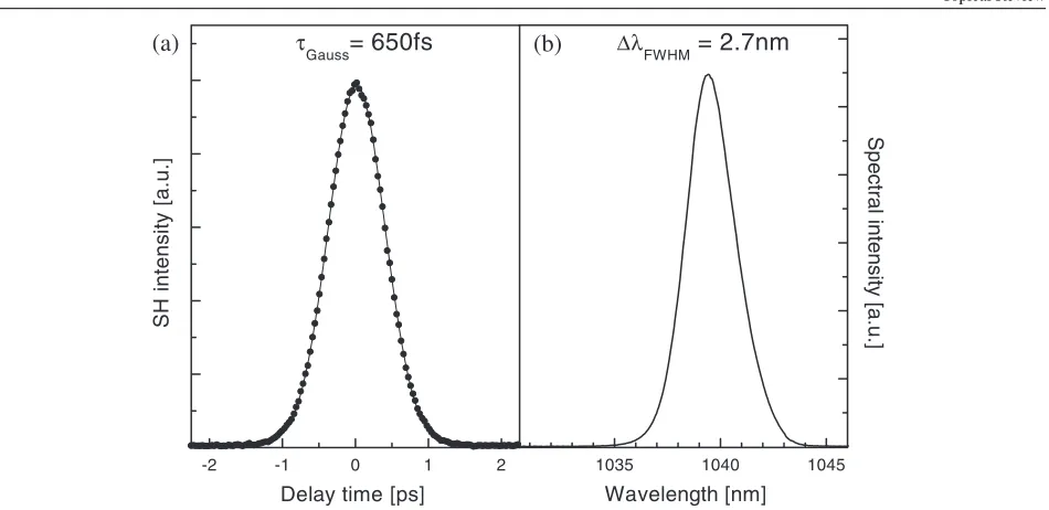
-2 -1 0 1 2 1035 1040 1045
τGauss
= 650fs
Delay time [ps]
∆λFWHM
= 2.7nm
Wavelength [nm]
(a)
(b)
S
H
intensity
[a.u.]
[image:9.595.64.539.76.307.2]Spectral intensity [a.u.]
Figure 4.(a) Intensity autocorrelation of 1.2 GHz pulse train from a VECSEL mode-locked by a SESAM operating in the optical Stark
effect region. The solid curve is a Gaussian fit to the data points, duration 650 fs FWHM. (b) Optical spectrum of these pulses, with 2.7-nm
(0.75 THz) FWHM.
pulses formed by a mode-locked edge-emitting diode. A key requirement for the formation of such chirp-free pulses is control of group dispersion delay (GDD) in the gain and SESAM structures, and the structural design features by which this was achieved are described in [29]. The negative self-phase-modulation in the SESAM was balanced by fine adjustment of the GDD in the gain structure to create quasi-soliton pulses. The overall cavity GDD at the 1040-nm centre wavelength of the pulses shown in figure 4 is small and positive, with a value of roughly +500 fs2. The pulses
generated by this laser evolve in a complex way as the operating wavelength is tuned thermally over a 1030–1050 nm band; both Gaussian and hyperbolic secant profiles are observed, and the shortest pulses have a duration <480 fs. It is likely that several mechanisms contribute to the pulse-forming process; fast saturable absorber mode-locking related to the optical Stark effect; slow saturable absorber mode-locking related to the resonant SESAM response; and the soliton mechanism discussed in [47]—with the relative contribution of the different mechanisms varying rapidly over the tuning range.
As we have seen, the high differential gain of semiconductor quantum wells leads to the onset of significant gain saturation in these lasers at much lower intra-cavity pulse fluences than would be required to saturate the gain of an impurity-doped dielectric medium. One consequence is that SESAM-mode-locked VECSELS are relatively free from the Q-switching instabilities that are exhibited by broad-band dielectric gain media such as lanthanide-doped glass and become increasingly severe at high repetition rates [48]. This phenomenon presents a challenge to the development of the compact, transform-limited optical pulse generators at repetition rates of 10 GHz and above that are desirable for applications such as high data rate transmission [49]. Hooglandet al[50] have shown that it is comparatively straightforward to generate sub-500-fs solitons
from a VECSEL at a repetition rate of 10.014 GHz. This device used the same SESAM and gain structure designs as in [29] to generate 486-fs pulses, with a short 15-mm-longV-cavity to achieve the high repetition rate. At an average power of 30 mW the pulses were 1.04×transform-limited, with a peak power of ∼6 W, and the laser showed no tendency towards Q-switching instability.
All the SESAM-mode-locked VECSELs described so far in this section have been optically pumped InGaAs/GaAs lasers operating around 1µm. To complete the story to date, we must note the recent reports of an electrically pumped SESAM-mode-locked VECSEL at 1µm as well as an optically pumped 1.5-µm mode-locked VECSEL. The electrically pumped device incorporates a gain structure of the type described in [15] into an external Z-cavity, with a repetition rate of 1.1 GHz. This device generated hyperbolic secant pulses of 57-ps duration at an average power of∼40 mW [51]; both fundamental and second harmonic mode-locking were observed. The authors observed that the long pulses resulted from spectral filtering in the high finesse cavity around the active region. More recently, Jasimet al[30] have used the same gain structure to generate 15-ps pulses at repetition rates up to 15 GHz. The SESAM in this device was a reverse-biased InGaAs multiple quantum well structure, and a microlens was used to couple the gain and absorber structures within the short plane/plane cavity, ensuring circular TEM00output.
reason, however, why a 1.5-µm mode-locked VECSEL should not generate quasi-soliton pulses in the sub-500-fs regime.
5. Future prospects
In conclusion, it seems possible that VECSELs will in the future be applied increasingly to the sort of task for which a diode-pumped solid state laser is currently used but where the wavelength, or another specification, is more easily met by a quantum well gain medium. Active mirrors are thinner than laser rods; therefore it is possible to make highly compact VECSEL devices, even with quite complex cavities. Injection pumping is clearly an option for medium power devices, where the application justifies more elaborate wafer design and fabrication. Optical pumping, however, is the most straightforward way in which to achieve a uniform carrier distribution over a large aperture; it is likely to remain the method of choice at the highest power output levels. In particular, it allows the gain structure to be optimized for optical performance, without the compromises imposed by the need for good electrical characteristics. The alignment tolerance for VECSEL optical pumping is less stringent than that required, for example, to launch light into single-mode fibre.
We have highlighted two particular areas of application for VECSELs: first as frequency-doubled short wavelength sources, of which some examples are already available as commercial devices, and second as compact sources of ultrashort pulses. This second area is less mature; however, it has demonstrated the potential for passively mode-locked VECSELs to generate near-transform-limited pulses of<500 fs duration directly from the laser oscillator, without external compression. With the proven power-scaling properties of VECSELs, it appears likely that such a laser might generate pulses of duration a few hundreds of femtoseconds at an average power of several watts. This source might be used, for example, as a compact and relatively inexpensive pump for continuum generation in microstructured fibre. Passively mode-locked VECSELs are inherently complementary to their solid state counterparts in that they are well-adapted for stable operation at fundamental repetition rates of∼10 GHz or more, suited to applications such as high bandwidth communication and optical clocking and sampling.
Whereas early work on VECSELs often used laser cavities and techniques similar to those developed for dye lasers, researchers now exploit the distinctive capabilities of the VECSEL gain medium increasingly to develop powerful new device geometries, such as the microchip VECSEL. The possibilities of a standing-wave laser medium containing gain and absorption as spatial delta functions are limited only by the precision to which structures can be grown and have as yet barely been explored. In the future it is likely that active mirrors will integrate gain together with other nonlinear and spectral filtering functions, allowing the development of ultracompact devices with sophisticated performance.
Acknowledgments
The authors are grateful to Isabelle Sagnes and Veronique Thierry-Mieg of CNRS Bagneux, France and John Roberts
of the III-V Facility at the University of Sheffield, UK for growing wafers for them and providing many invaluable technical insights. Much of the work reported here has arisen from a long and fruitful collaboration with Ursula Keller, R¨udiger Paschotta, and other members of their group at ETH Z¨urich. The authors have benefitted greatly from the input of former group members: Suki Dhanjal, Pierre Suret, Kestutis Vyˇsniauskas, and Johnson Xin. They also acknowledge the support of the Engineering and Physical Sciences Research Council of the UK, to whom Hannah Foreman and Keith Wilcox are indebted for their studentships.
References
[1] Innerhofer E, Sudmeyer T, Brunner F, H¨aring R,
Aschwanden A, Paschotta R, Honninger C, Kumkar M and
Keller U 2003Opt. Lett.28367–9
[2] Le H Q, Dicecca S and Mooradian A 1991Appl. Phys. Lett.58
1967–9
[3] Kuznetsov M, Hakimi F, Sprague R and Mooradian A 1997
IEEE Photon. Technol. Lett.91063–5
[4] Holm M A, Burns D, Cusumano P, Ferguson A I and
Dawson M D 1999Appl. Opt.385781–4
[5] Garnache A, Kachanov A A, Stoeckel F and Houdre R 2000
J. Opt. Soc. Am. B—Opt. Phys.171589–98
[6] Holm M A, Burns D, Ferguson A I and Dawson M D 2000
Proc. CLEO-US 2000 (San Francisco)pp CTHJ-7
[7] Kuznetsov M, Hakimi F, Sprague R and Mooradian A 1999
IEEE J. Sel. Top. Quantum Electron.5561–73
[8] H¨aring R, Paschotta R, Aschwanden A, Gini E,
Morier-Genoud F and Keller U 2002IEEE J. Quantum
Electron.381268–75
[9] Alford W J, Raymond T D and Allerman A A 2002J. Opt.
Soc. Am. B—Opt. Phys.19663–6
[10] Hastie J E, Hopkins J M, Calvez S, Jeon C W, Burns D, Abram R, Riis E, Ferguson A I and Dawson M D 2003
IEEE Photon. Technol. Lett.15894–6
[11] Hastie J Eet al2003Electron. Lett.391324–6
[12] Lutgen S, Albrecht T, Brick P, Reill W, Luft J and Spath W
2003Appl. Phys. Lett.823620–2
[13] Zakharian A R, Hader J, Moloney J V, Koch S W, Brick P and
Lutgen S 2003Appl. Phys. Lett.831313–15
[14] Chilla J, Butterworth S, Zeitschel A, Charles J, Caprara A,
Reed M and Spinelli L 2004Photonics West: Solid State
Lasers XIIISan Jose, CA
[15] McInerney J Get al2003Electron. Lett.39523–5
[16] Mueller M, Linder N, Karnutsch C, Schmid W, Streubel K P,
Luft J, Beyertt S, Giesen A and Doehler G H 2002Proc.
SPIE4649265–71
[17] Park S H, Kim J, Jeon H, Sakong T, Lee S N, Chae S, Park, Y,
Jeong C H, Yeom G Y and Cho Y H 2003Appl. Phys. Lett.
832121–3
[18] Garnache A, Hwang W Y, Hoogland S, Martin W, Koulikov S, Permogorov D, Tropper A C, Paldus B and Kachanov A A
2002Proc. IEEE 14th Indium Phosphide and Related
Materials Conf.pp post-deadline paper 3
[19] Hoogland S, Garnache A, Sagnes I, Paldus B, Weingarten K J, Grange R, Haiml M, Paschotta R, Keller U and Tropper A C
2003Electron. Lett.39846–7
[20] Sagnes I, Le Roux G, Meriadec C, Mereuta A, Saint-Girons G
and Bensoussan M 2001Electron. Lett.37500–1
[21] Symonds C, Sagnes I, Garnache A, Hoogland S,
Saint-Girons G, Tropper A C and Oudar J-L 2003Appl.
Opt.426678–81
[22] Kondow M, Kitatani T, Nakatsuka S, Larson M C,
Nakahara K, Yazawa Y, Okai M and Uomi K 1997IEEE J.
Sel. Top. Quantum Electron.3719–30
[23] Calvez S, Burns D and Dawson M D 2002IEEE Photon.
[24] Hopkins J M, Smith S A, Jeon C W, Sun H D, Burns D, Calvez S, Dawson M D, Jouhti T and Pessa M 2004
Electron. Lett.4030–1
[25] Cerutti L, Garnache A, Genty F, Ouvrard A and Alibert C
2003Electron. Lett.39290–2
Garnache A 2004 Private communication
[26] Holm M A, Ferguson D and Dawson M D 1999IEEE Photon.
Technol. Lett.111551–3
[27] Holm M A, Cusumano P, Burns D, Ferguson A I and
Dawson M D 1999CLEO ’99
[28] Hoogland S, Dhanjal S, Tropper A C, Roberts J S, H¨aring R,
Paschotta R, Morier-Genoud F and Keller U 2000IEEE
Photon. Technol. Lett.121135–7
[29] Garnache A, Hoogland S, Tropper A C, Sagnes I,
Saint-Girons G and Roberts J S 2002Appl. Phys. Lett.80
3892–4
[30] Jasim K, Zhang Q, Nurmikko A V, Ippen E, Mooradian A,
Carey G and Ha W 2004Electron. Lett.4034–6
[31] Garnache A, Kachanov A A, Stoeckel F and Planel R 1999
Opt. Lett.24826–8
[32] Bertseva E, Kachanov A A and Campargue A 2002Chem.
Phys. Lett.35118–26
[33] Picque N, Guelachvili G and Kachanov A A 2003Opt. Lett.28
313–15
[34] Iwai M, Yoshino T, Yamaguchi S, Imaeda M, Pavel N, Shoji I
and Taira T 2003Appl. Phys. Lett.833659–61
[35] Paschotta R, Moore N, Clarkson W A, Tropper A C,
Hanna D C and Maze G 1997IEEE J. Sel. Top. Quantum
Electron.31100–2
[36] Kozlovsky W J, Lenth W, Latta E E, Moser A and Bona G L
1990Appl. Phys. Lett.562291–2
[37] Birkin D J L, Rafailov E U, Sokolovskii G S, Sibbett W,
Ross G W, Smith P G R and Hanna D C 2001Appl. Phys.
Lett.783172–4
[38] Raymond T D, Alford W J, Crawford M H and Allerman A A
1999Opt. Lett.241127–9
[39] Schiehlen E, Golling M and Unger P 2002IEEE Photon.
Technol. Lett.14777–9
[40] Rafailov E U, Sibbett W, Mooradian A, McInerney J G,
Karlsson H, Wang S and Laurell F 2003Opt. Lett.28
2091–3
[41] Jiang W B, Shimizu M, Mirin R P, Reynolds T E and
Bowers J E 1993IEEE Photon. Technol. Lett.523–5
[42] Xiang W H, Friberg S R, Watanabe K, Machida S, Jiang W B,
Iwamura H and Yamamoto Y 1991Opt. Lett.16
1394–6
[43] Jiang W B, Mirin R and Bowers J E 1992Appl. Phys. Lett.60
677–9
[44] Watanabe K, Iwamura H and Yamamoto Y 1993Opt. Lett.18
1642–4
[45] H¨aring R, Paschotta R, Gini E, Morier-Genoud F, Martin D,
Melchior H and Keller U 2001Electron. Lett.37
766–7
[46] Garnache A, Hoogland S, Tropper A C, Gerard J M,
Thierry-Mieg V and Roberts J S 2001CLEO Europe 2001
(Munich)
[47] Paschotta R, H¨aring R, Garnache A, Hoogland S, Tropper A C
and Keller U 2002Appl. Phys. B—Lasers Opt.75
445–51
[48] Honninger C, Paschotta R, Morier-Genoud F, Moser M and
Keller U 1999J. Opt. Soc. Am. B—Opt. Phys.16
46–56
[49] Krainer L, Paschotta R, Lecomte S, Moser M, Weingarten K J
and Keller U 2002IEEE J. Quantum Electron.38
1331–8
[50] Hoogland S, Tropper A C and Roberts J S 2003CLEO 2003
[51] Jasim K, Zhang Q, Nurmikko A V, Mooradian A, Carey G,