vertical-external-cavity surface-emitting lasers in different cavity configurations
.
White Rose Research Online URL for this paper:
http://eprints.whiterose.ac.uk/151379/
Version: Accepted Version
Article:
Avrutin, Eugene orcid.org/0000-0001-5488-3222 and Panajotov, Krassimir (2019)
Delay-differential-equation modeling of mode-locked vertical-external-cavity
surface-emitting lasers in different cavity configurations. Materials. ISSN 1996-1944
[email protected] https://eprints.whiterose.ac.uk/
Reuse
Items deposited in White Rose Research Online are protected by copyright, with all rights reserved unless indicated otherwise. They may be downloaded and/or printed for private study, or other acts as permitted by national copyright laws. The publisher or other rights holders may allow further reproduction and re-use of the full text version. This is indicated by the licence information on the White Rose Research Online record for the item.
Takedown
If you consider content in White Rose Research Online to be in breach of UK law, please notify us by
Materials 2019, 12, x; doi: FOR PEER REVIEW www.mdpi.com/journal/materials Article
1
Delay-differential-equation modeling of
mode-2
locked vertical-external-cavity surface-emitting lasers
3
in different cavity configurations.
4
Eugene A. Avrutin1 and Krassimir Panajotov2,3,*
5
1 Department of Electronic Engineering, University of York, York, UK; [email protected]
6
2 Faculty of Engineering Sciences, Brussels Photonics Team B-PHOT, Vrije Universiteit Brussel, 1050
7
Brussels, Belgium; [email protected]
8
3 G. Nadjakov Institute of Solid State Physics, Bulgarian Academy of Sciences, 1784 Sofia, Bulgaria
9
* Correspondence: [email protected]; Tel.: +32-2629-3567
10
Received: date; Accepted: date; Published: date
11
Abstract: A simple, versatile model for the dynamics of electrically and optically pumped
vertical-12
external-cavity surface-emitting lasers mode locked by semiconductor saturable absorber mirror is
13
presented. The difference between the laser operation in the linear and folded cavity, as well as
14
the potential for colliding pulse operation, are studied.
15
Keywords: vertical-external-cavity surface-emitting lasers; mode locking; SESAM; frequency combs
16
17
1. Introduction
18
Vertical External-Cavity Surface-Emitting Lasers (VECSELs) first developed in 1997 [1] have the
19
advantage of the mature VCSEL technology for the semiconductor gain chip consisting of an epitaxial
20
Distributed Bragg Reflector (DBR) and several Quantum Well (QW) or Quantum Dot layers. This
21
allows wavelength flexibility, output power scalability and mass production. The external cavity
22
makes possible lasing to occur in a single transverse and longitudinal mode by implementing,
23
respectively, spherical mirrors and Fabry-Perot filters in the external cavity [1-5]. On the contrary,
24
multi-transverse mode lasing is typical for VCSELs with output power in excess of several mW due
25
to spatial hole burning [6, 7]. Spectral coverage of VECSELs extends from 390 nm [8] to 5 m and
26
even to 244 nm [10] by an intracavity fourth harmonic generation. By efficient thermal management
27
the output power is scaled by simply scaling the area of the optically pumped spot reaching 100W in
28
CW operation [11]. VECSELs are very well-suited for mode-locked operation by utilizing
29
Semiconductor Saturable-Absorber Mirror (SESAM) either in the external cavity [12] or integrated in
30
the gain-chip [13]. Tremendous progress has been achieved since the first demonstration of an
31
SESAM mode-locked VECSEL in 2000 [14]: the pulse durations in fundamentally mode locked
32
operation has been decreased to 107 fs [15] and even to 60fs in a burst operation [16], the average
33
output power has been increased to 6.4W [17] and the peak power increased to 4.35 kW [18]. While
34
the shortest pulses have been achieved with optically pumped active layers, electrically pumped
35
structures are promising for a number of applications versatile but fairly complex theoretical
36
model has been presented [19, 20 ] for mode locking in electrically pumped VECSELs, but only for
37
the simplest linear geometry and using a semi-microscopic model for the optical properties of
38
Quantum-Well active layers. Later, a delay-differential model of a similar type but with a simpler
39
gain model was used for inclusion of complex transverse/lateral effects in a MIXCEL structure, in
which the active layer and the saturable absorber are hosted within the same chip [21], with a
41
possibility to substantially enhance computational efficiency by narrowing the temporal window
42
when simulating the pronounced ML regime [22]. In recent papers [23,24], a version of a
delay-43
differential model was developed taking into account the folded, as well as simple linear, cavity
44
geometries. These papers centred on lasers designed for ultrashort pulse generation and were mainly
45
dedicated to the issue of multiple pulse (pulse molecule) generation observed under some operating
46
conditions in such lasers; therefore the gain chip and saturable absorber were treated essentially as
47
short travelling-wave amplifiers, ignoring their reflective nature and resonator properties (indeed,
48
for femtosecond pulse generation it is beneficial to suppress the resonator properties of the chips by
49
applying antireflection coatings, to minimise any narrowing of the emission spectra).
50
An alternative to the delay-differential equation modelling is an iterative pulse shaping
51
approach [25,26,27], where gain, saturable absorption, and dispersion in each round trip are, as in
52
classic mode locking theories, represented by pulse shaping operators in time or frequency domain,
53
as appropriate. Such an approach is by necessity somewhat artificial as it separates dispersion from
54
gain and absorption and also effectively assumes a unilateral ring cavity. Still it has proven very
55
useful for many cases of practical significance, particularly when the main limitation for the pulse
56
duration is the group velocity dispersion of the cavity (soliton mode locking regime). With simulation
57
parameters deduced from measurements for a known laser, such a model is capable of providing
58
very good agreement with experiment in both picosecond [26] and femtosecond [27] regimes;
59
however it may be not the most appropriate for describing regimes and designs where more than one
60
pulse can exist in the cavity, and for including the cavity parameters at the design stage.
61
Here we continue the work started in the earlier conference papers [28] and present a model
62
based on an approach similar to that of [19, 20] and so treating the cavity properties of the gain and
63
absorber chip consistently, but using a simpler, generic active layer model that can be used for both
64
linear and folded-cavity geometry. The model can be, and is in this study, applied to study different
65
regimes of laser operation, including the possibility of colliding pulse and multiple colliding pulse
66
mode locking, and also can be used for inclusion of polarization effects in future.
67
The paper is organized as follows. In section 2 we present the derivation of the model and its
68
application to a straightforward linear cavity. Sections 2 and 3 deal with different versions of a folded
69
cavity, with either gain or the absorber forming the central chip. Finally, in section 4 a brief
70
discussion and summary are presented.
71
2. Vertical External-Cavity Surface-Emitting Laser: time-delay model.
72
2.1. Derivation of a simple equation for the active cavity dynamics.
73
A schematic of the mode-locked VECSEL consisting of vertical-cavity amplifier chip (left side)
74
and a SESAM chip (right side) is shown in Fig. 1.
75
L
L
ad
gd
aL
ext ir
ir
0 iaFigure 1. Mode-locked VECSEL consisting of vertical-cavity amplifier chip with two DBRs with
76
reflectivities r0 and r1 and active region with thickness dg and a SESAM chip with a single DBR and
77
active region thickness da. L and La are their effective lengths and Lext is the length of the external
78
cavity.
79
The derivation of the model is a somewhat simplified version of that of [19] and is shown here for
80
completeness. As in [19], we start with the frequency domain approach and then convert it into time
81
domain The equation for the reflected field more accurately wave amplitude leaving the gain chip
82
reads
83
2 2 ( )
2 ' '
1
j kL
g i o
r g inc j kL i inc rc i inc i o
t r Ge
E r E r E E r E
r r Ge
, (1)
In this equation:
84
Eincis the complex amplitude of the incident field.
85
Erc is the complex amplitude of the field exiting the active resonator chip into the passive compound
86
cavity.
87
ri and ro are the (wavelength-dependent) reflectances of the mirrors of the resonator facing inside
88
(i.e. the incident light) and outside the cavity ri is the reflectance seen by the light incident on the
89
mirror from the external cavity side, which has the same amplitude as ribut different phase, as usual.
90
L is the geometric cavity length.
91
k is the complex wave vector. We can define a reference frequency and the corresponding wave
92
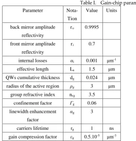
vector kref n ref c
- for convenience it is easiest to assume that ref is the frequency of one of the cold
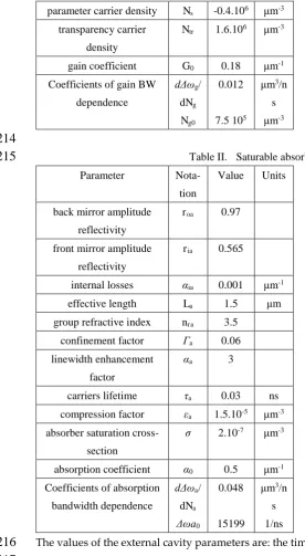
93
cavity modes. Then, int
2
ref
n j
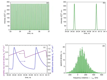
k k
c
,
intbeing the internal loss in the passive part of the94
resonator.
95
G
is the single-pass dimensionless complex gain by all the QWs in the active layer of the resonator.96
Assigning the active layer a thickness La and introducing the equivalent distributed complex gain
97
'
''
g
g
jg
we can writeG
e
g gdg
e
gL, where the total confinement factor, including the98
enhancement, or relative confinement, factor due to the standing wave profile g is
99
/
g
d
gL
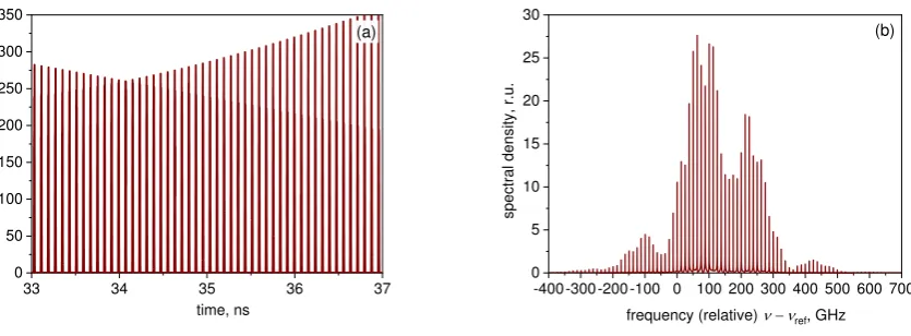
(2)This formalism is most natural in the case of a relatively thick, distributed, gain region, in which case
100
the standing wave factor is g=1. In the case of one or several QWs, when dg<<L, the notion of g is
101
somewhat artificial, but can be introduced heuristically alongside a g value of 1<g<2 (see below).
102
Using lumped gain per well, as in [19], is more rigorous (e.g. it gives g>1 self-consistently), but also
103
more complex, particularly in the case of multiple Quantum Well (QW) or Quantum Dot (QD) active
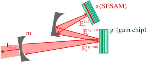
104
layers separated by a substantial distance (e.g. located in different wave antinodes). The present
105
formalism, in principle, applies to an arbitrary active layer thickness and location, though in this
106
paper we shall concentrate on the most usual one using a thin active layer in a single resonant
107
location.
108
The usual differential equation for an injected laser (i.e. a vertical cavity amplifier with two strongly
109
reflecting mirrors, operated above or near lasing threshold) is obtained by taking the absolute value
of the denominator in eqn. (1) to be small (which means operating above or near threshold, and
111
simultaneously with a small frequency detuning from the cold cavity mode frequency). In the more
112
general case of a resonator with arbitrary reflectances (in electrically pumped VECSELs, reflectances
113
of 70-90% can be used [19, 20]), we cannot assume the absolute value of the denominator in eqn. (1)
114
to be small but can assume small frequency detuning
2
nL
G
net1
c
. Then,115
2
1
r r Ge
i o j kL
1
G
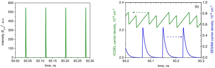
net
jT G
rt net
,
(3)where
116
G
net
exp
g L
net
r r
i oexp
g
int
L
cG
(4)is the complex net roundtrip gain, with
117
c
r r
i oexp
intL
(5)the (real) cavity attenuation factor. We have also introduced the round trip time of the cavity which,
118
as usual in the theory of vertical cavity structures, is evaluated as rt
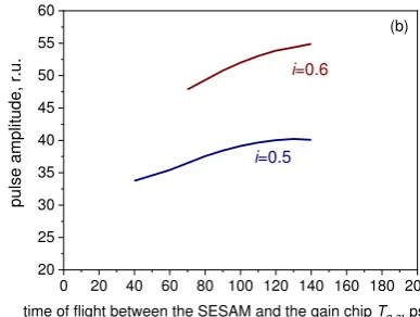
2
g effn L
T
c
, whereng n dnd
119
is the group refractive index, and eff
arg
oarg
i
g
c d
L
L
r
r
n d
is the effective cavity length.120
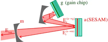
Then, the resonator equation becomes
121
' 21
G
netjT G
rt net
E
rct t r Ge
i i o j kLE
inc
. (6)The active layer in a VECSEL is always thin so
G
is never high above one (indeed, the measured122
chip reflectance has been reported [29,30] as Rg=|rg|2 for ri andRg forri notations as in
123
Eq. 1)), from which the value of |
G
|-1 can be estimated to be of the order of 10-2 at most, meaning it124
is safe to approximate in Eq. (6)
125
1
,
G
G
G
gL
Strictly speaking, the expression (6) includes the dispersion of both the VECSEL active subcavity and
126
the complex gainGG(
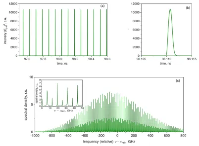
). If (as is usually the case) the operating wavelength is near the gain peak,127
we can use a Lorentzian gain spectrum approximation with a width g.
128
Then, assuming as usual
g, the usual substitution j d dt gives a single differential
129
equation for the determination of the field reflected from the cavity
130
1
+
' intg rc L
rt c c rc i i o inc
g
f
G dE
T
G
E
t t r e
E
dt
(7)where
G
gL
is evaluated at the reference frequency
ref and1
1
(
) /
g
ref p g
f
j
131
represents the carrier density dependent detuning between
ref and the spectral peak
p of gain.132
In a QW active material, the carrier density dependence of the detuning is weaker than in bulk
133
material so we can take fg=1=const. The equation combines cavity selectivity and gain dispersion
and thus can, in general, describe the performance of a gain chip with arbitrarily small or large
135
reflectances. In electrically pumped VECSEL designs, however, typically |ri| > ~ 0.5 [19,30], so, for
136
realistic semiconductor active media ( g>~1013s-1) we can comfortably assume that the spectral
137
selectivity of the cavity dominates over the gain dispersion:
138
rt c
g
gL
T
Thus in the first approximation, we can neglect gain dispersion and write the equation in the simple
139
form
140
1
+
' intLrc
rt c c rc i i o inc
dE
T
G
E
t t r e
E
dt
(8)Equations (7) and (8) are the main result of this section.
141
142
2.2. The full mode-locked laser model: the linear cavity.
143
To consider the full cavity, we need to recall that with a single incident and single reflected beam in
144
the linear cavity,
145
( )
'
g
r rc i inc
E
E
r E
(9)and note that
146
( )
(
)
'
a
inc r ext
E
E
t
T
w
(10)where Text= Lext/c is half of the round-trip time of the external cavity, and
E
ra is the field reflected147
from the absorber chip,
is the dimensionless attenuation between the chips (including theout-148
coupling, if it is located between the chips, and the attenuation in the contact layer of an electrically
149
pumped VCSEL), defined for the intensity as usual, hence square root in the equation for the field
150
amplitude. Technically speaking, the value needs to be complex, with the phase dependent on the
151
sub-wavelength variation in the length Lext of the internal cavity, but in the linear cavity this can be
152
set to zero with no loss of generality. The dimensionless parameter w >1 is the ratio of the beam
153
cross-section diameters in the gain (broader) and absorber (tighter to ensure saturation).
154
The absorber chip itself in the linear cavity can be described as in [19] by equations symmetric to
155
those of the gain chip, with the incident field given by
156
( ) ( )
'
(
)
a g
inc r ext
E
w E
t
T
(11)( ) ( ) ( )
'
a a a
r ia inc rc
E
r
E
E
. (12)Here, the field reflected from the inside of the chip is, assuming a (detuned) Lorentzian absorption
157
spectrum, evaluated using an equation formally identical to (7):
158
int, ( )
( ) ( ) ( )
1
'
a aa
L
a a rc a a
rt ca ca rc ia ia oa inc
a
f A dE
T
A
E
t t r e
E
dt
As in the case of the gain chip,
ca
r r
ia oaexp
intL
, r0a and ria being the outer and inner159
reflectances of the absorber cavity,
T
rt( )a is the SA cavity round-trip time, and the absorption in the160
cavity, evaluated at ref, at is quantified as
161
a a
A
L
. (14)he detuning factor
1
1
(
) /
a
ref pa a
f
j
needs to take into account that the SA is typically162
operating at the spectral slope of the absorber (
ref
pa) /
a~1.163
The complex gain and absorption in the case of bulk or QW active layers (QD layers may need more
164
complex analysis) can be parametrized using the phenomenological concepts of gain and absorption
165
compression coefficients
g ,
a , and linewidth enhancement factors for the carrier-dependent166
gain and absorption
H,
Haand the nonlinearities
,
a:167
1
( ) 1
g H g g
g g
g g N j S
S
(15)
1
( ) 1
a Ha a a a
a a
N j S
S
(16)
where Sg,a are the effective photon densities in the gain and absorption chip active layers. To write
168
out the rate equations for carrier densities in both chips, we need the explicit expressions for these
169
quantities, which depend on the geometry. Since
G
1,
A
1
, we can estimate the field in170
the active layer of both chips in the passive resonator approximation. In the case of active layers in
171
the form of (single or multiple) thin (QW or QD) layers very near the field antinodes, which we shall
172
follow in the analysis below, we can write
173
Sg= 2 ( ) int
g
E
, Sa= 2 (a) intE
, (17)where the fields inside the gain and SA active layers are evaluated assuming a resonant QW position
174
as
175
( ) ( )
int
0
1
g o g
rc i
r
E
E
t r
; int( ) (a)1
a oa
rc ia oa
r
E
E
t r
(18)From these expressions, the enhancement factors can be evaluated as
176
2 2
( ) (a)
2 2
0 0
1
1
;
1
1
o oa
g
a
r
r
r
r
(19)which in the case of |
r
o|~1 gives(g)≈2, the well-known result for the wave enhancement factor in an
177
isolated VCSEL cavity with the QW active layer at the resonant position.
In the case of distributed (multilayer of bulk) gain or absorbing layers occupying a substantial fraction
179
of the cavity, the enhancement factors could be taken as ≈1, with the intensities calculated as
180
2
( ) 21
g/
g o rc i
S
r
E
t
,
2 2 (a)
1
/
a oa rc ia
S
r
E
t
but that case is not considered here.The effective photon densities Sg,a then are used in the carrier rate equations:
181
( ) =
( ) 1
g g g g
g g g g g g
dN j N g N
S dt ed N S
v
(20)
(
)
=
(
)
1
g p a
a a
a
a a a a
N
dN
N
S
dt
V
S
v
, (21)
where as usual
v
g=c/ng,
a(
V
a)
is the absorber recovery time, Va being the (reverse) bias applied182
to the chip, if any. For the carrier dependences of gain and absorption, in this paper we use the
183
standard phenomenological expressions
184
0
( ) ln g s
p g
tr s
N N
g N G
N N (22) 0 ( )
p Na Na
(23)The dependences of gain and absorption bandwidths (BW) on respective carrier densities are estimated
185
in the first approximation as linear, i.e.
186
0
( ) g( ),
g g g g
g
d
N N N
dN
0
( ) a .
a a a a
a d N N dN
2.3. The main observable parameters.
187
It is useful to establish the relations between parameters used in the model and the measurable
188
values typically quoted in experiment, such as the threshold of laser operation, the saturation fluence
189
of the absorber, and the modulation contrast of the SA chip.
190
The threshold condition of the compound cavity is given by a transcendental equation which in our
191
notations is written as
192
0
2
2 2 2
2 0
2 2
0
'
'
1
1
1
a inrercavity a j kL j kLj k L
i o th ia oa
i ia
j kL j kL
th i o ia oa
t r G e
t r A e
r
r
e
G r r e
A r r e
(24)where
G
th
1
G
th andA
0
1
A
0are (complex) threshold gain and unsaturated absorption,193
and 0 ref k k c
the wave vector in vacuum at the resonant (modal) frequency. The threshold
194
condition is taken as the lowest gain of all the multiple solutions of the transcendental equation (24),
195
which correspond to modes of the compound cavity. The numerical solution of essentially the same
196
problem, though in different notations, illustrates [19] that, since the cavity length Linrercavity>>L, La, the
197
modes are spaced closely enough for there always to be a few near the resonance of both chip
198
resonators, essentially allowing us to count 20
1
inrercavity
j k L
e
. In that case, assuming that the gain chip199
and SESAM are resonant cavities, we can establish an analytical estimate for the threshold in the form
1
1
int
1 1 1
ln 1 i oA 1
th th th
oA i o
r r L
g G G
L L L r r r
(25)
where
201
2
0
0
1
'
1 1
ia ca a la a
oA ia
i ca a la a
t a f L
r r
r a f L
(26)
is the unsaturated SA chip reflectance.
202
The saturation fluence of the absorber in the model we use (Eq.(23)) is
203
2
0
1
1
ia oa
sat
ia oa
A r r F
t r
(27)
The reflectance contrast is estimated most easily neglecting the self-phase modulation in the SA (since
204
the Henry factor in the absorber is usually believed to be smaller than in the amplifier) and assuming
205
small detuning from resonance, in which case
206
2
0 2
2 2
1
ia ca
sA sA oA sA a a
ia ca
t
R r r r r a L
r
(28)
where
207
2
'
1
ia ca
sA ia
i ca
t
r
r
r
(29)is the amplitude reflectance of a fully saturated absorber.
208
2.4. Numerical Results.
209
The gain-chip and the saturable absorber parameters used in this section, unless specified
210
otherwise, are listed in tables I and II, respectively.
[image:9.595.72.341.504.783.2]211
212
Table I. Gain-chip parameters
213
Parameter Nota-
Tion
Value Units
back mirror amplitude
reflectivity
ro 0.9995
front mirror amplitude
reflectivity
ri 0.7
internal losses i 0.001 m-1
effective length La 1.5 m
QWs cumulative thickness dg 0.024 m
radius of the active region g 3 m
group refractive index nrg 3.5
confinement factor g 0.06
linewidth enhancement
factor
g 3
carriers lifetime g 1 ns
parameter carrier density Ns -0.4.106 m-3
transparency carrier
density
Ntr 1.6.106 m-3
gain coefficient G0 0.18 m-1
Coefficients of gain BW
dependence
d g/
dNg
Ng0
0.012
7.5 105
m3/n
s
m-3
[image:10.595.44.321.73.577.2]214
Table II. Saturable absorber parameters
215
Parameter Nota-
tion
Value Units
back mirror amplitude
reflectivity
roa 0.97
front mirror amplitude
reflectivity
ria 0.565
internal losses ia 0.001 m-1
effective length La 1.5 m
group refractive index nra 3.5
confinement factor a 0.06
linewidth enhancement
factor
a 3
carriers lifetime a 0.03 ns
compression factor a 1.5.10-5 m-3
absorber saturation
cross-section
2.10-7 m-3
absorption coefficient 0 0.5 m-1
Coefficients of absorption
bandwidth dependence
d a/
dNa a0
0.048
15199
m3/n
s
1/ns
The values of the external cavity parameters are: the time of flight between the gain and the absorber
216
cavities ns the transmission coefficient and the ratio of the beam cross-section diameters
217
onto the gain and the absorber chips = 3.
218
219
Figures 2-4 present an example of simulated mode-locked operation of a VECSEL SESAM
220
configuration. Long- and short-term time traces of photon density
|
E
rc(a) 2|
are shown in Fig. 2 (a)221
and (b), respectively. Fig. 2(c) shows the transient of carrier densities Naand Ng corresponding to the
222
photon density transient of Fig. 2(b). The optical spectrum of the time trace of Fig. 2 (a) is shown in
223
Fig.2 (c).
33 34 35 36 37 0
50 100 150 200 250 300 350
intensi
ty
|
E
(a) rc
|
2.
a.u.
time, ns
(a)
34.00 34.02 34.04 34.06 34.08 34.10 34.12 34.14 0
50 100 150 200 250 300 350
intensi
ty
|
E
(a) rc
|
2.
a.u.
time, ns
(b)
225
34.00 34.02 34.04 34.06 34.08 34.10 34.12 34.14 4.0
4.5 5.0 5.5 6.0
SE
SA
M
carrier
densi
ty
Na
,
10
18
cm
-3
ampli
fier chip carr
ier densi
ty
Ng
,
10
18 cm
-3
time, ns
(c)
-0.2 0.0 0.2 0.4 0.6 0.8 1.0 1.2 1.4
-200 0 200 400 600 0
5 10 15 20
spectral densi
ty,
r
.u.
frequency (relative) n nref, GHz
(d)
226
Figure 2. Time traces of the long-term (a) and short-term (b) evolution of the photon density
227
reflected from the SESAM chip. (c) the corresponding evolution of the carrier densities; (d) the
228
spectrum of (a). Gain chip current ic=0.6 mA (stable mode locking).
229
As the modification of the pulse by a single round-trip is only moderate in the ML VECSEL, the pulse
230
shape is fairly symmetric; however the up-chirp usual in passively mode locked semiconductor lasers
231
is still present, if relatively modest, with the time-bandwidth product of n0.6 (the pulse duration
232
and the spectral width n being evaluated at half maximum) at the current shown. The chirp also
233
manifests itself in the asymmetry and some envelope modulation of the spectrum.
234
235
The evolution of the pulse duration and amplitude with current is illustrated in Fig, 3 a and b
236
respectively. the pulse duration is in the picosecond range and, as in [19], decreases overall with
237
current. As normal in mode-locked semiconductor lasers (see [32,33] and references therein), the
238
pulses become longer with an increase in the absorber relaxation time.
[image:11.595.68.518.92.429.2]0.3 0.4 0.5 0.6 0.7 0.8 2
3 4 5 6
pu
lse
duration
(FWHM), ps
current, "mA"
a=10 ps
20 ps
(a)
0.3 0.4 0.5 0.6 0.7 0.8
0 1 2 3 4 5 6 7
pu
lse a
mp
liude
, "
mW"
current, "mA"
leading edge instability
(b)
[image:12.595.81.515.90.244.2]240
Figure 3. Current dependences of the pulse duration (a) and amplitude (b). In (b), the absorber recovery time
241
is 10 ps.
242
243
As in [19 no trace of the trailing edge self-pulsing instability was observed in our simulations; this
244
can be attributed to both the relatively low repetition frequency and the weak pulse modification per
245
pulse However at high currents the irregular leading edge instability in the form of two or at
246
higher currents, several non-periodically competing pulse trails (Fig. 4a) is present; its onset has been
247
chosen as the upper extent of curves in Figure 3a.
248
249
33 34 35 36 37
0 50 100 150 200 250 300 350
intensi
ty
|
E
(a) rc
|
2.
a.u
time, ns
(a)
-400 -300 -200 -100 0 100 200 300 400 500 600 700 0
5 10 15 20 25 30
spectral densi
ty,
r
.u.
frequency (relative) n nref, GHz
(b)
250
Figure 2. Time traces of the long-term evolution of the photon density reflected from the SESAM
251
chip (a) and the corresponding spectrum (b). Gain chip current ic=1.2 mA (unstable operation)
252
As in edge-emitting ML lasers, the spectral signature of this unstable regime is the spectral shape
253
(Fig. 4b) less regular and with more envelope modulation than the spectrum of stable ML (Fig. 2b).
254
3. VECSEL SESAM in a folded geometry.
255
3.1. Formulation of delay-differential model for the folded cavity
256
In this section, we consider the case of geometry alternative to the linear one treated in [19] and the
257
previous section the folded geometry In this case the three reference points of the cavity Fig. 5)
258
are the output mirror (m), the gain chip (g) and the SESAM (a).
[image:12.595.83.501.419.573.2]261
262
Figure 5. Mode-locked VECSEL –SESAM in folded geometry with an additional mirror.
263
264
The purpose of the intermediate fully reflecting mirror is essentially for establishing the correct
265
value of the width ratio w.
266
267
In the folded cavity designs realised so far [21] it is the gain chip that is located in the middle of the
268
cavity (Fig. 5). In this case, the equation for the SESAM chip remains the same as Eq. (13),
269
int,
( )
( ) ( ) ( )
1
'
a aa
L
a rc a a
rt ca ca rc ia ia oa inc
dE
T
A
E
t t r e
E
dt
, and we still have270
( ) ( )
'
(
)
a g a
inc r a g
E
w E
t
T
(30)where Ta-g= La-g/c is the flight time between the gain and absorber chips, and
E
r(ga) is the field271
reflected from the absorber chip in the direction of the gain chip.
272
For the gain section, the equation is functionally different, taking into account reflections in two
273
directions. For the field leaving the cavity towards the output mirror, we would have
274
int
( )
(g ) ( )
1 '
g m
L
m a g
rc
rt c c rc i i o inc
dE
T G E t t r e E
dt
(31)
The total field measured near the gain chip and propagating towards the output mirror then is
275
( ) ( ) ( )
'
g m a g g m
r ia inc rc
E
r
E
E
(32)For the field leaving the cavity towards the SESAM, we have
276
int
( )
( ) ( )
1 '
g a
L
g a m g
rc
rt c c rc i i o inc
dE
T G E t t r e E
dt
(33)
The total field travelling from the VECSEL gain chip towards the SESAM then is
277
( ) ( ) ( )
'
g a m g g a
r i inc rc
E
r E
E
(34)Finally, the field returning to the gain chip from the mirror is
278
( ) (g )
(
2
)
g m
j
m g m
inc m m r g m
E
r
e
E
t
T
(35)with Tg-m the flight time between the gain chip and the mirror, and the factor
e
jg m taking into279
account wavelength-scale cavity length variation. The field returning to the gain section from the
280
SESAM will be the same as in the linear cavity:
281
(g m) r
E
(g a)
r
E
out
E
(SESAM)
a
(gain chip)
g
m
( )a
( ) ( )
( )
'
g
a g a
inc r g a
E E t T
w
(36)
The output field at the time t then is given by
282
(g m)
(
),
1
2out m m r g m m m
E
t
E
t T
t
r
(37)For the carriers in the VECSEL gain cavity we have the rate equation identical to (20), but the intensity
283
in the cavity is now due to propagation in both directions. In the plane wave approximation and, as in
284
[23,24], assuming in this study incoherent addition of the counter propagating signals (applicable given
285
a wide enough aperture) the intensity within a thin resonantly positioned gain layer is
286
2
2 2
(g ) (g )
1
o a mg rc rc
i
r
S
E
E
t
(38)3.2. Results of the simulations for the folded cavity.
287
288
Figure 6 illustrates the dynamics of the photon (a) and carrier (b) densities in a short folded cavity,
289
with
T
g a
T
m g
40 ps
, corresponding to the repetition rate of 12.5 GHz (in the example shown,290
25 ps
g a
T
, Tm g 15 ps). As in the case of the linear cavity, there is only one pulse in the cavity291
per round trip; however the pulse is amplified in the gain chip twice per round-trip, which thus has
292
substantially shorter time to recover than in a linear cavity with the same overall length.
293
93.0 93.1 93.2 93.3
2.0 2.2 2.4
SE
SA
M
carrier
densi
ty,
10
18 cm
-3
VC
SE
L carr
ier densi
ty,
10
18
cm
-3
time, ns
(b)
0.0 0.2 0.4 0.6 0.8 1.0
[image:14.595.91.513.432.566.2]294
Figure 6. dynamics of the photon (a) and carrier (b) densities in a short folded cavity
295
296
Figure 7 shows the pulse duration and amplitude for the case of a short folded cavity as functions of
297
the gain chip current. As in the linear cavity, and as is typical in all mode-locked semiconductor
298
lasers, the pulse duration is somewhat longer for longer absorber recovery time. The current
299
dependence of the pulse duration in this case is non-monotonic, decreasing with current at lower
300
currents, as predicted also by [19] as well as by early generic theories of ML lasers with weak pulse
301
modification per pulse (see e.g. [31]), but increasing at higher currents, when pulse modification per
302
pulse is more significant, in common with most edge-emitting ML lasers [32,33]. As in Fig.3, the
303
upper limit of the curves is set by the onset of leading-edge chaotic instability.
304
93.00 93.05 93.10 93.15 93.20 93.25 93.30 0
100 200 300 400 500 600
intensi
ty
|E
g-a
|
2.
a.u.
0.2 0.3 0.4 0.5 0.6 1.0
1.2 1.4 1.6 1.8 2.0
a= 10 ps, Tga= 25 ps, Tgm=15 ps a= 20 ps, Tga= 25 ps, Tgm=15 ps a= 10 ps, Tga= Tgm=20 ps
pu
lse d
ur
atio
n,
ps
current, "mA"
(a)
0.3 0.4 0.5 0.6
0 2 4 6 8 10 12 14
aborber recovery time
a= 10 ps
a= 20 ps
peak
power
,
"mW"
current, "mA"
(b)
[image:15.595.90.506.88.231.2]305
Figure 7. Current dependences of the pulse duration (a) and amplitude (b) in a short folded cavity.
306
307
For the relatively high repetition rate shown in Figures 6-7, the pulse parameters show almost no
308
dependence on the relative length of the two branches of the cavity, so long as Tg a Tm g is kept
309
constant (note the rectangular dots in Figure 7a). This is understandable, because given
310
,
g a m g g
T
T
, the recovery of the population inversion in gain chip (strictly speaking, exponential)311
is virtually linear and so the total depletion of the gain chip by both pulses does not depend on the
312
relative magnitudes of the flight times
T
g a,
T
m g . This dependence becomes more pronounced in313
longer cavities, when the flight times approach
g by order of magnitude. This is illustrated in [image:15.595.121.506.475.624.2]314
Fig. 8, calculated for
T
g a
T
m g
200 ps
, or the repetition rate of 2.5 GHz. As seen in the figure,315
there is an optimal relation of the cavity branch lengths in this case yielding the shortest ML pulse
316
width, which, at least for the values of reflectances studied, corresponds to the gain chip near the
317
middle of the cavity.
318
0 20 40 60 80 100 120 140 160 180 200 10.0
10.5 11.0 11.5 12.0 12.5 13.0 13.5
i=0.6
i=0.5
mode locki
ng pul
se duration, ps
time of flight between the SESAM and the gain chip Tg-a, ps (a)
0 20 40 60 80 100 120 140 160 180 200 20
25 30 35 40 45 50 55 60
i=0.5
i=0.6
pu
lse
amplitud
e, r.
u.
time of flight between the SESAM and the gain chip Tg-a, ps
(b)
319
Figure 8. Dependences of the pulse duration (a) and amplitude (b) in a long folded cavity
320
(Tg a Tm g 200 ps) for two values of current
321
322
At relatively high currents, close to the onset of the leading edge instability, the geometry affects the
323
stability limits: with the lengths of the branches strongly unbalanced, the gain chip current limit of
324
stability is lower (the extent of the curves in Fig. 8 corresponds to stable single-pulse emission limit).
[image:15.595.321.515.476.622.2]4. Colliding-pulse mode locking configuration.
329
330
4.1. Time-delayed model
331
We consider last an alternative, and so far hypothetic, case of the central chip being the SESAM, with
332
the gain chip and the mirror m terminating the cavity, which is more difficult to realise (and has not,
333
to the best of our knowledge, been realised in this form so far) but offers greater functionality,
334
potentially offering Colliding Pulse Mode locking (CPM) option. The equation system for this case
335
is obtained from one for the folded cavity with the gainchip in the middle by simple permutation of
336
the symbols g and a in the notations.
337
[image:16.595.190.407.241.326.2]338
Figure 9. Colliding-pulse Mode-locking folded geometry.
339
340
Indeed, in a folded cavity with the SES“M in the middle the equation for the gain chip remains the
341
same as eqn. (8)
342
1
+
' intLrc
rt c c rc i i o inc
dE
T
G
E
t t r e
E
dt
and we still have
343
( )
(
)
'
a g
inc r a g
E
E
t
T
w
(39)where Ta-g= La-g/c is the flight time between the gain and absorber chips, and
E
r(ag) is the field344
reflected from the absorber chip in the direction of the gain chip.
345
For the SESAM, the equation is functionally different, taking into account reflections in two
346
directions. For the field leaving the cavity towards the output mirror, we would have
347
348
int
( )
( ) ( ) ( )
1
'
a m
L
a rc a m g a
rt ca ca rc ia ia oa inc
dE
T
A
E
t t
r e
E
dt
. (40)The total field towards the output mirror then is
349
( ) ( ) ( )
'
a m g a a m
r ia inc rc
E
r
E
E
(41)For the field leaving the cavity towards the gain (VECSEL) chip, we have
350
int
( )
( ) ( ) ( )
1
'
a g
L
a rc a g m a
rt ca ca ca rc ia ia oa inc
dE
T
A
E
t t
r e
E
dt
. (42)The total field travelling from the SESAM towards the VECSEL chip then is
351
( ) (m ) ( )
'
a g a a g
r ia inc rc
E
r
E
E
. (43)Finally, the field returning to the SESAM from the mirror is
352
(a m) r
E
(a g) r
E
out
E
(gain chip) g
(SESAM) a
m
(g) r
( ) ( )
(
2
)
a m
j
m a a m
inc m m r a m
E
r
e
E
t
T
(44)whereas the field returning to the SESAM from the gain section will be the same as in a linear cavity:
353
(g ) ( )
'
(
)
a g
inc g r g a
E
w E
t T
. (45)The output field at the time t then is given by
354
( ) 2
(
),
1
a m
out m m r a m m m
E
t
E
t
T
t
r
(46)Inside the SESAM cavity we still have the same rate equation but the fields exist due to propagation in
355
both directions. In the plane wave approximation and with a thin resonantly positioned absorber,
356
2
2 2
( ) ( )
1
oa a g a ma rc rc
ia
r
S
E
E
t
(47)The absorber saturation fluence in the folded cavity, with either absorber position, would be the same
357
as in the linear geometry (though effectively in the colliding pulse design it will become twice smaller
358
with 2 pulses arriving simultaneously), and the threshold condition in the CPM cavity becomes
359
2
int
2
1 1
1 1
1 i m oA m 1
th th
m oA m i o
r r r L
g G
L L r r r r
. (48)
4.2. Calculations and results.
360
Fig. 10 presents the schematic of evolution of the output photon density in a CPM configuration (a,
361
b) and the corresponding spectrum (c), for one operating current in a short (
T
g a
T
m g
40 ps
)362
cavity. The time-domain pulse trail (Fig. 10a) shows complete repetition frequency doubling
363
compared to a linear cavity (two pulses per round trip; note the identical amplitudes of adjacent
364
pulses and the repetition period same as in Figure 2 despite a twice longer cavity), as expected for
365
well developed CPM operation. However, in the spectrum, the doubling of frequency interval
366
between modes is not complete; intermediate modes corresponding to the round-trip of the entire
367
cavity are somewhat suppressed but still present (see inset to Fig. 10c). Similar performance was
368
simulated for edge emitting mode locked lasers under certain conditions [34].
369
97.6 97.8 98.0 98.2 98.4 98.6 0
2000 4000 6000 8000 10000 12000
[image:18.595.106.509.83.379.2] [image:18.595.79.527.556.708.2]in
tensity |
Eg-a
|
2.
a.u.
time, ns
(a)
98.105 98.110 98.115 0
2000 4000 6000 8000 10000 12000
g-a
time, ns
(b)
372
-1000 -800 -600 -400 -200 0 200 400 600 800 0
5 10
0 10 20 30 40 50
0 1 2 3 4 5 6 7 8
spectral densi
ty,
r.u.
n nref,, GHz
sp
ec
tral
de
ns
ity,
r.u.
frequency (relative) n nref, GHz
(c)
373
Figure 10 Mode-locked VECSEL SESAM-output mirror structure time traces of
|
E
g a|
2: (a) pulse trail374
and (b) single pulse. (c) shows the spectrum of the time trace of (a), with a fragment in an inset. Injection
375
current is j=1.1 mA; absorber recovery time a=10 ps.
376
Figure 11 shows the evolution of the CPM pulse duration and amplitude with current. In this
377
geometry, the simulated pulsewidth increases with current through the current range studied; as
378
mentioned above this is typical for edge emitting lasers and can be associated with relatively strong
379
modification of the pulse per round trip. In edge emitters, such a situation is associated with an
380
asymmetric shape with the longer trailing edge, which indeed is observed also in our simulations
381
(Figure 10b).
382
0.4 0.6 0.8 1.0 1.2 1.4 1.6 1.8 2.0 0.6
0.8 1.0 1.2 1.4 1.6
pu
lse
duration
(FWHM), ps
current, "mA"
(a)
0.6 0.8 1.0 1.2 1.4 1.6 1.8 2.0 10
15 20 25 30 35 40
pu
lse
ampliud
e, "mW"
current, "mA"
(b)
383
Figure 7. Current dependences of the pulse duration (a) and amplitude (b) in the CPM design. a=10 ps
The upper extent of the curve, as in Figures 3 and 7, is the onset of the leading edge instability. The
386
stability range for this design, with two pulses saturating the absorber simultaneously, is substantially
387
higher than in the case of a simple linear cavity with the same repetition rate, and the pulses, shorter,
388
by virtue of more efficient absorber saturation, which is one of advantages of CPM [32]. The cavity
389
thus looks suitable, in principle, for picosecond puse generation. In the case of the femtosecond
390
regime using a low-dispesion optically pumped active chip, the more complex, but also more reliable
391
ring CPM geometry used in recent studies [35] may be preferable (the folded cavity studied here
392
would need micrometer-scale balancing of subcavity lengths). More detailed investigation is
393
reserved for future work.
394
5. Conclusions
395
We have presented a simple, versatile model for the dynamics of electrically and optically
396
pumped vertical-external-cavity surface-emitting lasers mode locked by semiconductor saturable
397
absorber mirror. Time delays in the external cavities formed by the VECSEL gain chip and the
398
saturable absorber mirror and output mirror are accounted for. Analytical expressions for the
399
experimentally accessible characteristics of the system are provided, namely, the threshold gain and
400
saturation fluence and reflection contrast of the absorber. For realistic parameters of the
401
semiconductor cavities, the model predicts fundamental mode locking with ps pulse duration. The
402
dependences of the pulse width and pulse amplitude, as well as the frequency chirp are investigated
403
as a function of injection current. The model is easily generalized for different VECSEL and SA
404
configurations and examples for the case of folded geometry with central chip being either the gain
405
section or the SESAM are presented. Future work can concentrate on perfecting the model for the
406
folded cavities, including account of partly coherent addition of signals as in [35] and possibly the
407
lateral effects, as well as polarization properties and more diverse geometries.
408
409
Author Contributions: E. Avrutin and K. Panajotov developed the model, wrote the software and carried out
410
the simulations. Both authors participated in the writing, review and editing the manuscript.
411
Funding: This research was funded by Fonds Wetenschappelijk Onderzoek (FWO), grant number G0E5819N.
412
Acknowledgments: K. Panajotov acknowledges the Fonds Wetenschappelijk Onderzoek (FWO), grant number
413
G0E5819N and Methusalem foundation for financial support.
414
Conflicts of Interest: The authors declare no conflict of interest.
415
References
416
1. Kuznetsov, M., Hakimi, F., Sprague, R., Mooradian, A. High-power (>0.5-W CW) diode-pumped
417
vertical-external-cavity surface-emitting semiconductor lasers with circular TEM00 beams IEEE Photon.
418
Technol. Lett., 1997, 9, 1063 - 1065
419
2. Tropper, A.C., Foreman, H.D., Garnache, A., Wilcox, K.G., Hoogland, S.H., Vertical-external-cavity
420
semiconductor lasers, J. Phys. D: Appl. Phys.2004, 37, R75 R85.
421
3. Tropper, A.C. and Hoogland, S., Review: Extended cavity surface-emitting semiconductor lasers, Prog.
422
Quant. Electr.,2006, 30, 1-43.
423
4. Holm, M. A., Burns, D., Ferguson, A. I., Dawson, M. D., Actively Stabilized Single-Frequency
Vertical-424
External-Cavity AlGaAs Laser, IEEE Photon. Technol. Lett. 1999, 11, 1551-1552.
425
5. Lindberg, H., Larsson, A., Strassner, M., Single-frequency operation of a high-power, long-wavelength
426
semiconductor disk laser, Opt. Lett.,2005, 30, 2260-2262.
427
6. Chang-Hasnain, C., Harbison, J., Hasnain, G., Von Lehmen, A. Florez, L., Stoffel, N., Dynamic, polarization,
428
and transverse mode characteristics of vertical-cavity surface-emitting lasers, IEEE J. Quant. Electron.,1991,
429
27, 1402-1409.
430
7. Panajotov, K., Valle, A., Thienpont, H., Sciamanna, M., Polarization- and Transverse-Mode Dynamics in
431
Optically Injected and Gain-Switched Vertical-Cavity Surface-Emitting Lasers emitting lasers, IEEE Journ.
432
Quant. Electr.,2009, 45, 1473-1481.