Theses
Thesis/Dissertation Collections
2004
Generalized analytical model for RF planar
inductors using a segmentation technique
Marie Yvanoff
Follow this and additional works at:
http://scholarworks.rit.edu/theses
This Thesis is brought to you for free and open access by the Thesis/Dissertation Collections at RIT Scholar Works. It has been accepted for inclusion
in Theses by an authorized administrator of RIT Scholar Works. For more information, please contact
Recommended Citation
Approved by:
USING A SEGMENTATION TECHNIQUE
by
Marie Yvanoff
A Thesis submitted in Partial Fulfillment of the
Requirements for the Degree of
MASTERS OF SCIENCE
In
Electrical Engineering
Professor
Jayanti Venkataraman
(Dr.
Jayanti
Venkataraman
-
Advisor)
Professor _ _
S_a_n_t_o_s_h_K_o_K_u_ri_n_e_c __
(
Dr. Santo
s
h Kurinec -
Committee Advisor)
Professor
Syed Saifullslam
(Dr. Syed
I
s
l
a
m -
Committee Advisor)
Professor _ _
R_o_b_e_r_t _B_o_w_m_a_n
__
_
(
Dr. R
o
bert B
owman
- D
e
p
ar
tm
e
nt He
ad)
DEPARTMENT OF ELECTRICAL ENGINEERING
COLLEGE OF ENGINEERING
ROCHESTER INSTITUTE OF TECHNOLOGY
ROCHESTER, NY
DEPARTMENT OF ELECTRICAL ENGINEERING
COLLEGE OF ENGINEERING
ROCHESTER INSTITUTE OF TECHNOLOGY
ROCHESTER, NY
MAY, 2004
Title of Thesis:
GENERALIZED ANALYTICAL MODEL
FOR RF PLANAR INDUCTORS
USING A SEGMENTATION TECHNIQUE
I, Marie Yvanoff, hereby grant permission to Wallace Memorial Library of Rochester
Institute of Technology to reproduce this thesis in whole or in part. Any reproduction will
not be for commercial use of profit.
/01.;-ACKNOWLEDGMENT
Many
people supported meduring
thecompletion ofthisthesis.First
of allI
wish to expressmy
sincere gratitude tomy
advisor;Dr.
Jayanti
Venkataraman.
Her
help,
support, guidance and encouragements were pricelessthroughout this work.
Not only is
she anoutstanding
professor, sheis
an even greaterperson.
Thanks
also to the committee members,Dr. San
toshKurinec
andDr. Syed Islam for
reviewing my Thesis.
Next,
I
wantto thankmy
co-workersin
theMicromagnetic
group,Cody
Washburn,
Tejas
Jhaveri
andGary
Fino
advisedby
Dr.
Kurinec.
Thanks
also tomy
colleaguesin
theFields
Lab,
Lakshmi
Achutha,
Jeff Mc.Figgins
andMike Seymour
andfor
keeping
avery
enjoyable
working
atmosphereandhelping
me wheneverI
needed.I
wouldlike
toshowmy
gratitudetomy
family
for
theirkindness
and support.It's
toughto
be away from home.
Last
but
notleast,
I
wouldlike
to thankmy best
friend,
Omar
for
alwaysbeing
here
whenI
neededhim. I
wouldhave
turnedcrazy
without you.Shoukran.
ABSTRACT
The
planar coilinductor has become
avery
critical circuit componentin RF
mixedsignalapplicationwhere
it
can reside either onthepackage orin
thechip.However,
thereis
no clearmethodology
toaccurately
analyze thebehavior
oftheinductor
over abroad
range of
frequencies
andfor obtaining
a particular physicallayout
for
a required value ofinductance. At
present,it has been done
by
full
wave solvers, approximate quasistaticanalysis, and
lumped
element equivalent circuits, each withits
own advantages andlimitations. This
work presents an analytical modelbased
on a segmentation methodin
conjunction with a
Green's function for
a power/ground plane model.This
methodhas
been
used to obtain analytical closedform
solutionfor
planar coilinductors
of twopopular shapes,therectangularand circular configurations.
The
modelincludes
a ground plane and the coil configuration such asspacing
andline
width, and the materia] characteristic such asconductivity
ofthemetallayer
andthedielectric
parameters.It is
afrequency
dependant
solution thatincludes
the resonant modesin
thecavity formed
by
the
inductor
and the ground plane.This
methodhas been
appliedsuccessfully
torectangular and circular coil
inductors
ofdifferent dimensions
where thereis
excellentagreement with
full
wave solvers.Inductors
on a package andin
achip have
been
fabricated
and experimental results show excellent agreement to predicted valuesobtained
from
thisanalytical work.Also
presentedin
thisworkis
a comparison of popularEM full
wave solvers and twoquasistaticmethods, theadvantagesand
limitations
of eachhave been
discussed.
TABLE
OF
CONTENTSAcknowledgment
i
Abstract
ii
Table
ofContents
iii
List
ofFigures
vList
ofTables
vi1.
Introduction 12. Contributions
andMotivation
ofPresent Work
2.1 Contributions 4
2.2Organization ofThesis 5
3.
PlanarInductor,
On
Chip
andInPackage
3.1 Coilparameters 7
3.2Coilcharacterization 10
4.
Analytical Model4.1 Segmentation Technique 15
4.2 Rectangular Coils Inductor 20
4.2. 1
Green
'sfunction
ofRectangularopen cavities 224.2.2 Impedancematrix 23
4.2.3 Considerations
for
convergenceissuesfor
analytical model 244.3 Circular Coils Inductor 34
4.3.1 Green's
function
ofannularsector cavities34
4.3.2
Impedance
matrix37
4.3.3 Considerations
for
convergenceissuesfor
analytical model39
4.4
ImplementationoftheAnalyticalmodelfor
Planar Inductors43
5.
NumericalModeling
of planarInductor5.1 MaxwelBD
44
5. 1. 1
Setting
up
themodel45
5.1.2
Setting
up boundaries
46
5.2 High
Frequency
Structure Simulator
HFSS
48
5.3 Analysis
andSimulationofInductors
andTransformersfor
ICs 455.4
Current
sheetmethod49
5.5 ComparisonwithPublished
Results
50
5.6
Advantages
andlimitations
525.7 Ferrite Filled
Inductors
53
6. Results
6.1
Comparison
withHFSS
576.1.1
Planar
rectangular coil 586.1.2
Planar
circularcoil 606.2 ComparisonwithExperimental Results
62
6.2. 1
One-turn
rectangularcoil 626.2.2
Two-turn
rectangular coil 636.3 InvestigationofCoil Inductor
Geometry
for
alimitedfootprint
area 656.3. 11mpact ofnumberofturns, spacingandwidth 66
6.3.2Impact of
dielectric
thickness 697. Measurement
Techniques
7.1 Layout foroneport measurement 71
7.2 Layout
for
two-portmeasurement 727.3 Calibrationprocedure 74
7.4 Measurements
76
8. Conclusion
8.1
Summary
ofContributions for
thepresentWork78
8.
1.1Development
andvalidationof
analytical model78
8. 1.2
Computer
toolsassessment78
8.
1.3
On-chip
inductormeasurementtechniques 798.2 Future Work
79
References
81
List
ofFigures
1
-a) Rectangularcoil
layout,
b)
Circular
coillayout,
9
Inductorcrosssection,c)
On-chip,
andd)
Inpackage2-
Two
Port Microwave Network 10
3
- Equivalent Circuitfor
a2-portNetwork 1 1
4
-a) Planar Inductor
b)
CurrentsheetApproximation
[30]
1 1c)
Current
sheetSegmentationd)Inductor lines
Segmentation5- Rectangular
Coil b)Planar
Inductorb)Segmented
Inductorc)InterconnectMatrix 12
6-
Circular Coil b)Planar
Inductorb)Segmented
Inductorc)InterconnectMatrix 127
-a) Segmented Circular Coil
b)
Interconnect
Matrix 13
8- Planar
microwave circuit 21
9
- Rectangular Planarmicrowave circuit 22
10
-a) Rectangular Planarmicrowave circuit
b)
x-yplane/
port placements 241 1
-a)
Hoop
inductor
dividedinto
b)
4
segments andc) 7segments 2512- ComparisonofHFSS Results Vs Segmentation Method
for different
26number of segments
13
-a) inductor layout
b)
cross section view 27c)Comparison ofHFSS Results Vs Segmentation Method
14
-Interconnecting
Ports 2815
-a) Single
loop
inductorwithdielectricparameters:d =5pm,tan(8)=0,
er4 29b)
InductanceVsFrequency
Vsnumber ofPortdivisions
16
-a) Single
loop
inductorwithdielectricparameters:d =5um, tan(8)=0,er=430
b)
Inductance VsFrequency
for differentnumber ofPortdivisionsc)
Absolute
Percent Errorfor
Inductancefrom
Segmentation Results toHFSSresults17
Fringing
effects31
1 8
-a) Inductor Layoutwithdielectric: d =5um, tan(8)=0,sr=4 32
for different Numberof eigenmodes
b)
withN fixedat15 c)withMfixed
at7519-
Annular
sector34
20- Circular Coilgeneration:Exampleof2-turncircular
inductor
39
21
-a)
Two-loop
circularinductorb)
segmentedinductor
4022
-a)
Single
turncircularinductorb)
cross-section view41
c) Inductance Vs
Frequency
23-a)
Single
turncircularinductor
42
b)
Inductance Vs.Frequency
for different
value ofGreen'sfunction
eignenmodes24- Maxwell 3D Layoutwith
long
vias45
25
-MaxwelBD,
Layout- Closedloop
46
26- Silicon
IC
planarInductor50
27- Inductance Land
Q
([31]),
using MaxwelBDandHFSS
51
28- Example 1:
a) Planar Inductor
b)
HFSSandMomentum[31]
51
29
-Example 2: a) Planar Inductor
b)
HFSSandSONNET[32]
51
30
- Lumped Port Elementsetup
withHFSS53
f
31 - Ferrite
Permeability
Vs.Frequency
(Courtesy
FerronicsInc)
54
32-Ferrite
Loaded Micro-Inductor.(
t^
=l[xm,
tsio2
=2um,
tsi=33
- Inductance Vs. Ferritethicknessd
(um)
55
34
-a) Planar inductor
for
comparison withHFSS
b)
Reactance Vs.Frequency
58
35-a) Two-turnrectangular planar
inductor for
comparison withHFSS59
b)
Reactance Vs.Frequency
36
- Resultsfor
two turninductor
(fig34)
with adielectric
thicknessequalto300um59
Reactance
/
wVs.Frequency
for Comparison
withHFSS37
-a) Circular
inductor for
comparisonwithHFSSb)
Reactance Vs.Frequency
60
38-a) Circular
inductor
for
comparison withHFSS
b)
Reactance Vs.Frequency
61
39-a)
Milling
machineb)
Oneturninductor
constructed62
40-a) Planar
inductor for
comparison withExperimentalxesults63
b)
Cross
viewofInductorc)Reactance/
wVs.Frequency
41 2Turn Inductorconstructed
for
one port measurement63
42-a) Planar
inductor
for
comparison withExperimentalresults64
b)
Crossview ofInductorc)ReactanceVs.Frequency
43
- Fixedparametersa) Inductor Layout
b)
Cross-sectionview65
44-a) Reactancevs.
Frequency
67
b)
Quality
Factorvs.Frequency
for
avaryingnumber ofturns45
-a) Inductancevs.
Spacing
b) Quality
Factorvs.Spacing
68
Planarinductorgeometry:46
-a) Reactance Vs Width
b) Quality
Factorvs.Width69
47-a) Planar Inductor Layout
b)
cross-sectionview 70c) Reactancevs.
Frequency
for differentdielectric
thickness48- a-d): 2differentoptions of1 port configurationLayoutand cross-section view 72
49
-a-d): 2 differentoptions of2port configurationLayoutand cross-section view 73
50
-a-b):Testfixturewith OpenandShort Structures 74
51 - Measured
device
(DUT)
withParasitic 7552- Measured Open 75
53 - MeasuredShort 75
54- Planar Copper Microlnductor LayoutandCross-section View 76
55 - Network AnalyzerandProbe Station
Set-up
7656- ProbesandWafer 77
List
ofTables
Chapter 4:
1-Resistanceand Inductance Value
for different design
Configuration 511. INTRODUCTION
In early Si integrated
devices,
active components played a moreimportant
role thanpassive components.
Components
such astransistorshave been continuously shrinking in
size, while passive
devices have
remainedvery large
and placedexternally
ontheboard.
Technology
improvements have
enabledSi
circuits to operate athigher
frequency
[1]
where thecritical passive elements such as
inductors
are small enough tobe
realizedon-chip.
The
size of the circuitboard
has
also reduceddue
tofewer
external components.This has brought
a significant progress to personal communicationdevices
whereportability is
essential.The
use ofon-chip
passives such asinductive
elementsin
siliconradio-frequency
integrated
circuits allowedbetter
performancein Si low-noise
amplifiers[2]
[3],
distributeddc-dc
power converters[4],
mixersand oscillators[5]-[7].
Consequently,
it is
becoming
critical tobe
able to model thebehavior
of passivesover a
broad
range offrequencies
accurately,primarily
theinductor.
Analyzing
andmodeling
theinductance
introduces
manydifficulties. The
parameters ofinterest for
thedesign
ofinductors
areinductance
andquality factor
and also alimited
footprint
area.Unfortunately,
there are no simple analyticalformulations
todetermine
themaccurately.At
present,it has been done
by
full
wave solvers, approximate quasistatic analysis, andlumped
element equivalentcircuits,eachwithits
ownadvantages andlimitations.
The benefit
ofgenerating
a solutionusing full
wave solveris
toinclude
allelectromagnetic effects subject to
boundary
conditions.MaxwelBD,
High
Frequency
,
Structure
Simulator(HFSS)
and
MOMENTUM
are examples of such toolsbased
onand
time,
especiallyfor
complicated structures.They
merely
analyze a particularinductor
layout
anddo
not serve as practicaldesign tools,
sodesign
optimizationis
achieved
for
a givenfootprint
areaby
trial and error.Although
these arewidely
usedtools,
atpresent,thereis
no assessmentof and comparisonbetween
the tools tohelp
thedesigner
choose the appropriate softwaretool, best
suitedfor
thefrequency
range andphysical geometry.
Such
astudy
needstobe done.
As for
the quasistatic approach,Analysis
ofSi Inductors
andTransformers
for IC's
(ASITIC) [8]
has been developed specifically for
thedesign
ofon-chip inductors
andtransformer.
ASITIC
provides a quick analysis compared to the timeintensive
nature ofthe
full
wave solvers whileproviding
an equivalent circuit modelfor
the parasitics.However
portdefinitions
are not welldefined. The
procedurefor optimizing geometry
tomeet
design
constraints still relies upon a collection of approximatelumped-element
solutions, and several
iterations
are needed to get the optimumlayout
at a particularfrequency.
The
analyticalformulation
which uses coupledline
couplers and cornerdiscontinuities
[9],
proposed an approach to model rectangular spiralinductors. The
discontinuities
ofthe circuit such as thebends
are modeledusing
scalable models, andthe multiple coupled
lines
use adistributed
modelrelating
impedance
and admittancer
matrices.
Although
this model gives afrequency
dependent
solution,it
involves
avery
tedious and complicated
derivation
andis
therefore not suited as either an analysis orAnother
techniqueoriginally developed
by
Nguyen
andMeyer
[1]
for
the modelingofthe
inductor
useslumped
element circuit models which approximate the circuit withindividual
inductances,
resistances and substrate capacitances.Efforts have
alsobeen
madeto
improve
and understandthis techniquein
greater [10][12],
as well asintroduce
the
eddy
currentlosses
within the substrate[13]-[16],
skin effect and currentcrowding
[17]-[22].
It
finally
containedup
to22
elements[23]. While it usually
produces a rapidcalculation
dependent
on thefrequency,
any
changein
theinductor
requires anothermodeling iteration
beginning
withthecalculation of each parameter.Simple
formulas
for
planarinductors
without a ground plane asfrequency
independent
solutionhave
been
published[24]-[29]. Another
methodbased
on thecurrent sheet distribution
[30]
introduces
simple expressionsfor
spiralinductors
by
approximating
the sides ofthespiralby
a current sheet with uniform currentdistribution.
Although
these expressions give goodinsight
tohelp
thedesigner,
it
needs abetter
expression to take care of magnetic
coupling
to the substrate.It
also assumes that thecurrent
distribution
is
uniformin
all the conductors, whichbecomes
untrue athigher
frequency
with the skin andproximity
effects.The
majordisadvantages
are thatit does
not give a
frequency
dependant
expression anddoes
notinclude
ground plane andmaterial parameters.
It
is
vital,for
thedesigner
of anRF
circuit tobe
able to optimizeinductors.
And
despite
allthework andimprovement in
theresearchbeing
madefor
modeling
inductors,
there
is
still a critical needfor
a simple closedform
expressionfor
inductor design
that2. CONTRIBUTIONS AND MOTIVATION OF
PRESENT
WORK
The
use of embedded passive componentshas
the potential ofshrinking
the size ofcircuit
devices
and alsoreducing
their cost.Modeling
thebehavior
of passivedevices
accurately
and withthe minimum computation timehas become
critical.The
motivationofthispresent work
is
todevelop
a closedform
solutiontobe
used as a quickdesign
tool.The
formulation has
tobe
frequency
dependent
andhas
toinclude
a ground plane.The
design
tool presentedin
this workis
avery
useful tool that providesits independence
from full
wave solvers which arecomputationally
expensive to use.This
tool willbe
beneficial
for
applications with passive componentsbecause
it
provides afast
andaccurate solution.
2.1 Contributions
Major
contributionsfor
thisworkare asfollow:
1
.An
analytical modelhas been developed
with a closedform
solutionfor inductors
with
2
popularshapes,circularcoil and rectangular coil.The
methoduses a segmentationtechnique
in
conjunction with aGreen's function
of acavity
model.The
modelincludes
aground plane andthecoil configuration such as
spacing
andline
width, andthe materialcharacteristic such as
conductivity
ofthe metallayer
and thedielectric
parameters.The
results obtained are
frequency
dependent,
and canbe
extractedin
theform
ofS
andZ-matrices.
The input impedance
and thequality factor
oftheinductor
are extractedfrom
for
a wide range ofinductors
atdifferent frequencies. A design
methodologyis described
tooptimizethe
inductor layout for
agiveninductance
andfootprint
area.2. The
needfor assessing
variouscomputertools availabletodate has been
addressedin
thepresent work.The
four
populartools,
HFSS,
MaxwelBD,
ASITIC
andSONNET
have been
compared and the advantages anddisadvantages
of eachhave
been discussed
in
order tohelp
thedesigner
to choose thebest
suited tool.Defining
the nature andplacement of the port
is
critical.Comparisons have been
made withknown
examples[12][31][32]available
in
theliterature. Ferrite loaded
micro-inductorshave been
modeledtoobtain
higher quality factor
andinductance
valuesfor
alimited footprint
area.The
toolbest
suitedfor
thispurposehas been
suggested.3. Inductors have been fabricated
and experimental verificationshave been done in
ordertovalidatetheanalytical model.
2.2
Organization
The
following
chapter presents an overalldiscussion
onOn-Chip
andin-package
planar
inductor
characterization and configuration.The
analytical modelis developed in Chapter 3. The
techniqueusing
asegmentationmethod
in
conjunction with a ground/power plane modelis
fully
described. Green's
function for
reptangular shaped power plane and annular sector arederived in
detail.
Closed form
expressionsfor
theinductance for
each shape,rectangular andcircularhave
Chapter 4
presents an assessment ofthecommercially
available computer tools andlists
theiradvantages andlimitations in
ordertohelp
thedesigner
choosethebest
suitedtool.
Ferrite loaded
micro-inductorshave been
modeled.Chapter 5
presents the results wherethe analytical modelhas been
appliedto a widerange of planar
inductors. To
validatethetheory,
comparisonshave
been
made toHFSS
resultsand alsotoexperimental measurements.
Chapter 6 describes
thedifferent
measurement techniquesfor
On-Chip
Silicon IC
microinductors.
A
conclusion and contribution ofthe present workis
presentedin Chapter 7. Future
3. PLANAR INDUCTORS
ON-CHIP
AND IN
PACKAGE
3.1 Coil
parametersIt has been
seen that the use ofinductive
elementsin integrated
circuitsis
becoming
increasingly
important. As
the size ofintegrated
circuitsis continuously
shrinking,it is
becoming
critical tooptimizetheinductor layout. In
ordertooptimize aninductor
design,
allthe coil parameters and physical constraints needto
be
considered.The
parameters ofinterest
are theinductance
andquality
factor,
the objectiveis
to maximize thequality
factor for
a giveninductance
value.The first
constraintfor
thedesigner is
the maximumfootprint
area availableon thechip
orin
thepackage.Whether
theinductor is fabricated
on
chip
orin
the package, the other constraints are the material parameters, such asdielectric
and substratethickness,
permittivity,losstangent
and conductivity.The
first
parameter the
designer
has
to chooseis
a particularinductor
shape.For
an ease offabrication,
themost popular ones aretherectangular and circular coils.The
numbers ofturns,
width ofthelines,
andspacing between
thelines
alsohave
tobe
considered.In
orderto get a particular
inductance
for
a particularfootprint
area, there are an optimumnumber ofturns
for
a certain width andspacing
value.Experiment
and published workshow that the
increase in
theline
width resultsin
ahigher quality factor
and ahigher
inductance.
However,
skin effectbecomes
significant as this widthincreases.
The
increase in
theline spacing between
themetallines
resultsin
adecrease
in
the mutualinductance
andthereforein
the totalinductance,
suggesting
thatthespacing
shouldbe
asdetermined
by
its layout
and the specifications of the circuit to whichit is
part.The
parasitic elements
due
to thedielectric
and substrate parameters entailengineering
tradeoffs.
Thus,
it
is
critical tohave
an analyticalformulation
for
spiralinductors
in
ordertodetermine
an accurate valuefor
theinductance
andquality factor
topermitthedesigner
tochoosetheoptimal
inductor for
a given application.The
parameters thatneed tobe
optimizedfor
aninductor design
canbe
specifiedby
the
following
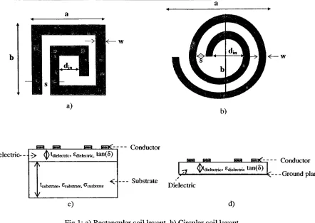
and shownin Figure 1
:1. Shape:
rectangular, circular,hexagonal,
octagonal.2.
Number
ofturns,
n3. Metal
width: w4.
Spacing
between
themetallines:
s5. Footprint
area(a,
b)
6. Dielectric layer,
thicknessoftheoxidetdieiectric,
Sdiekctrica)
b)
Dielectric-
-EM
iBlC-r--Conductor
>
^tdielecmc.
Edielectric, tan(8)^substrales^substrate,^susbtrate
**"" iwia
5L \^dielectric)Edielectrictan(d)
23
m^K----Conductor
Substrate
C Groundplane
Dielectric
c)
d)
Fig. 1: a)Rectangularcoil
layout,
b)
Circularcoillayout,
Inductorcross section,c)
On-chip,
andd)
InpackageFigure
LaandFigure Lb
showthelayout
for
rectangularand circular coillayout. The
inductor
canbe
realizedon-chip
(Fig.l.c)
orin
thepackage(Fig.l.d).Usually,
theplanarinductor
is
realizedonthetop
metallayer
toreducethecapacitancebetween
thesubstrateandthespiral.
It
canbe sitting
ontop
of adielectric
and substratelayer
whenit is
realizedon-chip, or on
top
of adielectric
and a ground planein
the package.On
the chip, thespace
below
theinductor is kept free
and notracesarepresent,due
totheelectromagneticfields
generatedby
theinductor.
The designer
has
thefreedom
toaddanother metallayer
and place a metal
layer
used as a ground planebelow
the oxidelayer.
Adding
anothermetal
layer
to the process andusing it
as a ground plane canbe
approximated as the [image:19.534.48.490.31.344.2]3.2 Coil Characterization
As
seenin Figure 1
a andb,
theinductor
canbe
representedas a2
portnetwork, withone port at the outer edge ofthe spiral and the other port at the
inner
edge.In
ordertogive a complete
description
ofN-port
network, thescattering
andimpedance
matrix areused.
An arbitrary 2-port
microwave networkis
considered and shownin Figure 2.
Portl Port 2
r+
[S]
\~+ ?
a)
v+
r
2
Portl >
Port 2
.7>
^
:
[Z]
X
b)
Fig.2: Two-port Microwave Network
In Figure
2a,
V~is
the amplitude ofthe voltage waveincident
on port n, andV
+
is
the amplitude ofthe voltage wave
reflecting from
port n.The scattering
matrix or[S]
matrix relates the
incident
and reflected voltage waves and gives a completedescription
ofthenetworkand
is defined
asthefollowing
for
a2-port
network:v:
S22
Sn
(D
Sr
is
the transmission coefficientfrom
portj
toporti.
Ss
is
the reflection coefficient atport
i
whentheother portis
terminatedby
a matchedload.
V,
Z
7
^11
^12
7
7
~22
^22
.(2)
Where
the totalvoltage andcurrentat porti
are givenby:
v.=v++vr
i i i
L=r-i:
(3a)
(3b)
Zy
is
the transferimpedance between
porti
and portj.
Zrt
is
theinput impedance
at portI
when alltheother ports are open-circuited.
The
[S]
matrixcanbe determined from
the[Z]
matrix and vice versa.From
theimpedance
matrixdefinition
(2),
the2-port
networkis described in
terms ofimpedance
parameters:V
=7J
+7J
V
=71+7
1
(4a)
(4b)
These
equationsleads
to theT
equivalent circuitas shownin figure 3:
'i
h
?
Zil
Zj2
-Z22
Z21
<. -.
Pdrtl
Zi2
v2
At
portl, theinput impedance
with port2
terminatedby
ZLis:
7
7
Z.
=Z- 12 21(5)
7+7
^22 TZyL
The input
impedance
can alsobe
written as:Z
=R
+jcoL
whereR
is
theinternal
resistance and
L
theinductance
of the coil.The
solutionfor
theinductance L is
thengiven
by
thefollowing:
LJMZJ
(6)
2?tf
The quality factor describes
thefrequency
selectivity
of a resonant circuit or cavity.In
the present work, where theinductor is
placed over a ground place, theQ
of theresulting cavity is
animportant
factor. The definition
ofQ
is based
on the maximumenergy
storedin
the electric and magneticfield
and average powerdissipated in
theconductors.
^ . . max
energy
storedQ
=2n*(7)
energy dissipated
percycle/>*
Q
=o)'w_+w.y
(8)
Where
Wm
is
the average magneticenergy
stored,We
the average electricalenergy
stored,
P,
thepowerloss,
T
theperiodand a) theangularfrequency.
At
resonance, theaverage stored magnetic and electricenergy
are equal, andthequality
2Wm
2W
P
P
1
1 11
Where
co^istheresonantfrequency
The
average magnetic storedenergy
and powerloss
aredefined
as:Wm=-LI
m2
P,=RI2
Substituting
(8)
and(9)
into
(7)
thequality factor becomes:
(9)
1
. T200)
01)
G3
=4.
ANALYTICAL
DEVELOPMENT
In previously
published work[30],
inductance
expressionshave been developed
where the planar
inductor
(FigAa)
has been
approximatedby
four
current sheets(Fig.4.b)
of equivalent currentdensities.
^.
fjurrerit direction
a)
b)
c)Fig.4: a) Planar
inductor
b)
Currentsheet approximation[30]
c) CurrentsheetSegmentationd)
Inductor Lines SegmentationBased
on the current sheet approximation[30],
thefirst idea for
the analyticaldevelopment
wastoapproximatetheplanarinductor
(FigAa)
and segmentit
asshownin
Figure 4.c. Each
segmentcontaining
a ground plane and adielectric
substrate canbe
viewed as a power/ground plane model.
This
model can thereforebe
chosen tocharacterize each
individual
segment with thefinal
model obtainedusing
a techniquedescribes later. Comparison
of these results with afull
wave solversindicated
that theinductor
needs tobe
model as shownin Figure 4.c
where thespacing between
thelines
needs to
be incorporated. This
means that each turn of theinductor
needs tobe
consideredas aseparate segmentas shown
in Figure 4.d.
For
this analytical model a segmentation methodusing
aninterconnecting
matrixis
used
in
conjunction with the wave model solution to the ground/power plane.By
thiscomputational time.
The
principle of the segmentation method as well as thecavity
model
for different
shaped circuitis
described
in
thischapter.4.1
Segmentation
techniqueIn
thiswork,a segmentation methodis
used thatis based
ondividing
thegeometry
ofthe
inductor into
rectangles andcombining
the characteristics ofthe segmented elementsby
aninterface
network thatincludes
spacing,line
width,dielectric
characteristic andground plane.
As
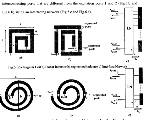
example, a2-turn
rectangularinductor
(Fig.5a)
and a2-turn
circularinductor
(Fig.6.b)
have been
segmentedinto
n segments.The
segments are connected viainterconnecting
ports that aredifferent
from
the excitation ports1
and2 (Fig.5.b
andFig.fj.b),
using
aninterfacing
network (Fig.5.candFig.6.c).
segmented
T ports
excitation
ports
Fig.5: Rectangular Coil a) Planar inductor
b)
segmentedinductor c) Interface Network aportl"portl
segmented aport2
ports Q_
bpon2
I.N
a)
b)
c) [image:25.534.47.502.283.665.2]The interconnect
matrixis
afictitious
network where the number of ports of theinterface
networkis
equal to the number of external ports(lp,2p)
plus the number ofsegmented ports.
The
external port piis
internally
connectedto the 1stport ofthematrixand the external port p2
is
directly
connected to the n port oftheinterconnect
matrix asshown
in Figure 7. The
matrixis
also used to represent all theinterconnection between
the
different
ports.As
anexample,for
the2
turninductor in
Fig.8,
the 1stsegmentSI
andthe 2nd segment
S2
are connected via2
links,
port2
is
connected toport4
and port3 is
connectedtoport
5,
theconnection are reportedinside
theinterconnect
matrix.(Fig.7.b).Portl
a)
b)
Fig.7: a) Segmented Circular Coil
b)
Interface NetworkThe
incideiitwaves oftheinterface
network aredefined
as: aJp, a2p,ai,a2,...,anandthe1?
K
2,
=KJ
2
b
- n _a - n _
(13)
Where
[S,
N
J
is
equal to1
when portsi
andj
areconnected, andis
equal to0
whenports
i
andj
are not connected or wheni
=j. The
matrix\Sj
NJexpresses
connectionbetween
segments.As
portlp
and2p
aredirectly
connectedin
theinterface
network toport
1
and nrespectively
(Fig.7.b).\S,
NJ
is
now expressed asfollows:
[sj=
0
0
\]
0
0
H,
2p
s.
ui(14a)
Where
V,
andV.,
are row vectors andV'
are column vectors
defined
by
IP(Fig.l4d-e).
yip=(10...0)
(14b)
V2
=(0...01)
2p
(14c)
V
=0
vOy
(14d)
V
=Y2P
0
vly
The
vectorV,
representstheconnection withthe external port pi and theother portsofthe
interconnect
matrix and theV2
represents the connections with the external port2p
andtheotherportsoftheinterconnect
matrix.The
final S-matrix
oftheinductor is
a(2x2)
matrixgiving
bip
andb2P
in
termsofonly
aip
anda2p.Because
the external ports portlp
and port2p
arerespectively
connected to port1
and n ofthe
interconnect
matrix,K
=a>
(15a)
b.
=a2p n
(15b)
Therefore,
equation(13)
canbe
rewrittenasin
(16).p,l
V
T
"0"
K
=[sj
a2
+0
a,
+ ip0
b
n _a
_ r._
0
1
a.
06)
The
matrix ofthesegmentaryunitsis defined
as(17a).
V
X
a2
=
lsc]
K
_an_
A.
where
lsc]=
S,
0
s2
0
s
(17b)
(Si,
S2....
Sn)
aretheS
matrices oftheindividual
segments, and are calculatedfrom
the
Z-matrices
(Zi,
Z2....
Z7)
corresponding
to theindividual
segmentsis
computed withthe ground/power plane model
described in
thefollowing
chapter.The resulting Z
matrices are transformed to
S-matrices
in
order to combine the segments through theinterface
network.Combining
(16)
and(17)
toeliminatetheb-vector,
we obtain:a.
a^
a
=
{[u-scsinnsc])
a]p
+([U-ScSinr[Sc])
a2pTo simplify
thenotation wedefine
thematrix[T]:
T
=[E-ScSinr[SJ
Where
U is
the'(nxn)
unit matrix.Substituting (15a)
and(15b)
into
(18)
We
canfinally
obtain:K=ai
=TnaiP+Tua2P
fe,
=a =T,a,+T
a,
2p n n\ \p rm 2p
(18)
(19)
(20a)
The final 2x2 S-matrix
oftheinductor
consists of a submatrix ofT
where thefour
elementsare at crosspoint
between
the 1standlast
column and 1stand
last
rows:[S]
=Tu
T.
11 \n
(21)
T.
T
_ n\ m
The resulting S
matrix of order of2
x2 is
convertedto theZ
matrix using:[z]
=([u]-[sy(Z0[uhZ0[s])
(22)
Where
Z0is
thecharacteristicimpedance.
By
thistechnique,
the characteristics of planar circuits are computedby
combining
those ofthe segmented elements.
Simple
expressionshave been developed
thatrequire avery
short computationaltime.For
thisparticularexample, theentire circuitis
atwoportcircuit.
The
same method canbe
usedfor
multiport circuit.4.2
Rectangular
coilsInductor:
The impedance
of atwodimensional
microwavecircuits observable at n ports canbe
expressed withthe
Green's function. The
(i,
j)
elementoftheimpedance
matrixis
givenin
(23)
-[33]:z*=^4rfte(*o)^
(23)
WfVV j WiWj
where
W\
andWJ
arethewidths oftheports.The
Green's function is
theimpulse
responseof a system and canbe
obtainedusing
awhen theshape ofthecircuit
is relatively
simple, andthecharacteristicsofthecircuit arederived using
equation(23).
For
a planar microwavecircuit, as shownin
Figure
8,
thebasic
equation todescribe
theelectromagnetic
field is
atwodimensional
waveequation,known
asHelmholtz
equation.Metal layer
-Dielectric layer
-->
^
d,
E^detan(5)< Groundplane
Fig.8: Planarmicrowavecircuit
The
solutions oftheHelmholtz
equation:(V2T+k2)G
=-jcojUdS(r~-70)
(24)
under given
boundary
conditions(magnetic
wallhave been
assumed at the periphery):dG
dn
=
0
(22)
are obtained.where JU
is
the permeability, CDis
theangularfrequency,
d
is
thedielectric
thicknessandk is
thewave number.n
is
thenormal'at
any
point ontheperiphery.The
timedependence exp(-j
0)t)
is
assumedfor
allfields
ontheplanar circuit.The Green's function
canbe
expressedin
terms oftheGCr.T.^ja.MdY^P-(25)
n
Where
kn
and0nare respectively
the eigenvalues and eigenfunctions of the waveequation
(V+fc2)G
=0.
COis
the angularfrequency,
p
thepermeability
andd
is
thethicknessofthe
dielectric.
In
thischapterthe solutiontoplanar circuits with simple shape as annularandrectangularwill
be discussed.
4.2.1
Green's
function forrectangular opencavitiesFor
the rectangularcircuit shownin Figure
9,
theboundary
conditions(22)
translateto the
following:
dG
dG
dx
;r=0,a
=
0
(26a)
oy
=
0
(26b)
y=0J>
Fig. 9: Rectangular Planarmicrowavecircuit
The
set offunction
thatsatisfy
theboundary
conditionsis
givenby
[33]:
C
C
#,(*.
y)=-f=-cos(kxmx)cos(kyny)(27)
|1
m=0
fl
n=0
where k =mnla,
k=n7rlb,
C
={ ,_C
=< ^-m
V2
m*0"
V2
n*0>71
The
resonantfrequency
canbe
writtenas:'
-sfe^^^-sfc
J[v)
+(t)
+(f
)
(28)
The
equationfor
the resonantfrequency
shows that thedominant
modeis
the onewiththesmallest
dimension. In
this case,thedielectric
thicknessd is electrically thin,
andthe
dominant
modes shouldbe
theonein
thex andy
directions,
so we arelooking
atthemnOmode.
This
is
why
thereis
no z-termin
equation(28).
The Green's function for
therectangular circuitbecomes
asin (29):
I
,_JCQpd
^ ^
2 2cos(/^x0)cos(/c^y0)cos(/cCT*)cos(^y)(29)
en*,y
\x0,y0)
2-1 2-1
"> ;2 , ; 2 ; 2 nh '><'m " hL
+kz
m represents them'th eigenmode
in
thex-direction and n represents then'th eigenmodein
the y-direction.k
represents the wave number,COis
the angularfrequency,
eis
thedielectric
permittivity,p
thepermeabilityandd
theheight
ofthedielectric.
Accounting
for
theloss in
thedielectric
material,thewave numberk is
givenin (30):
-^M-+3)
(30)
where r= ,
(31)
tan()
is
theloss
tangent ofthedielectric,
/
thefrequency,
and<7C
the conductivity ofthemetal
layer.
4.2.2
Impedance
MatrixSubstituting
(29)
into
(23)
andintegrating
over the port region, theijxh.
element oftheimpedance
matrixis
expressed asthefollowing
[37]:
Z-7
=ZZ
IZ^^ ^z^^^y^cos^x.Ocos^ypcos^^.)
m=0
tt"KkL+k-k<)
sm
k
^ii^-^IH^
sin
(
w^W
k^
W
.W_
k ^~
2
\
(32)
a and
b
are the metal plane widthsin
the x and ydirections
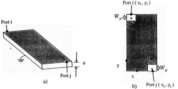
respectively.xi,yi,xj
andy.are the coordinates of the center
location
of theffh
andjth
ports. W^.W^W^-andW
arethefth
and/th port widthsin
thexandy directions.Porti
(
x;,yi)
Porti
[image:34.534.94.455.462.643.2]b)
Portj
(
xj,^)
4.2.3
Considerationsfor
convergenceissues for
analyticalmodelIn
order to achievebetter
results,different
parameters such as the numbers ofsegments,thenumber of port
divisions
in between
adjacent segments and thenumberofterms
in
the x andy
directions
canbe
optimized.This
sectioninvestigates
the value ofthese
different
variablesin
orderto geta good convergence.The
interest
ofthissectionis
not
only
to optimize thetechniquebut
also toimprove
the computertime ofthemethod.The
results ofthesegmentation method are compared withthoseobtainedfrom HFSS.
1)
Optimum Number
ofSegments:
The
numberof segments requiredis
adeterminant
parametertoget a good convergencefor
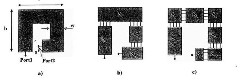
theinductor. Figure
11
showsdifferent
ways to segment a oneloop
inductor into
rectangles.
The
minimum numberofrectangles that are necessarytodivide
theinductor
is 4
asin Figure 1 1
.b.Another
way to segment theinductor is
to take account ofthecorner
discontinuities
andthelines
andtosegmenttheoneloop
inductor
with7
segmentsas
in Figure 1 1
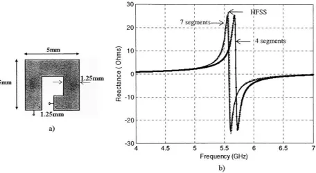
.c.-4 ?
1
fagS-b
IU
t >M' "farri As'
Portl p0rt2
a)
b)
c) [image:35.534.68.480.480.616.2]The
methodis
applied to a1
turninductor
coil shownin Figure 12.a. The
resultsshown
in Figure 12.b
compare theinductance
obtained withHFSS (dotted
line)
and thesegmentation method when the coil
is
segmented with either4
or7
segments.Even
though the method with
4
segments will computefaster
than the7
segments one, somediscrepancies
occurs withHFSS. The 7
rectangles segmentation shows perfectaccuracy
with
HFSS.
5mm
5mm
"
jllllllfe
.25mm
yu
* 1.25mm
a)
-30' '
5 5.5 6
Frequency (GHz)
[image:36.534.41.498.248.498.2]b)
Fig.l2:ComparisonofHFSS Results Vs Segmentation Method for differentnumber of segments
dielectric:d=5nm,tan(8)=0,^=4.
The
methodis
now applied to a2
turninductor
coil shownin Figure
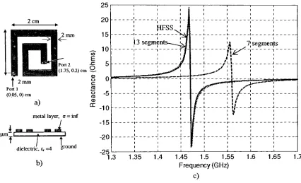
13.a. andin
Figure 13.b. For
aninductor
with2 turns,
the minimum numberof segments requiredis
equal to 7segments.
When
each comerdiscontinuities
are segmented, the number ofobtained with
HFSS
(dotted
line)
and the segmentation method when the coilis
segmented with either
7
or13
segments.The 13
rectangles segmentation shows perfectaccuracy
withHFSS.
When
the coilis only
segmented with7
segments,discrepancies
occur
in
frequency
as well asin
magnitude.?, fsst gsg i raft
t
r^r
dielectric,,=4 Sround
b)
-10
-15
-20
-25
ifflFSS
'
I
13 segments---^kl
\
' 7'segments
--v -frr
-r
"
H^|[-t-i--,J1
-1 ' / i i m
J W _
I t I I I i
/fi?Fr
I I 1 1 1 1 1 t 1 1[
;
1
:
t i ji r i i i
1.3 1.35 1.4 1.45 1.5 1.55
Frequency
(GHz)
c)
1.6 1.65 1.7
Fig.l3:a)
inductorlayoutb)
crosssectionviewc)ComparisonofHFSS Results Vs Segmentation Method for differentnumbersof segments
The
comparisonfor
theoneturn and 2-mminductor
withHFSS
showthattheresultscan
be incorrect if
theinductor
is
notproperly
segmented.The
results are even moreaffected when the number of turns
increases.
Adding
segments to model each cornerseparately
provides correctresults.In
conclusion, thenumberofsegments shouldinclude
one
for every
corner and onefor
each side.This is
toensurethatdiscontinuity
effects are [image:37.534.75.501.185.444.2]2)
Number
ofInterconnectPorts:
The
number ofPorts in between
theadjacent segmentsis
analyzedin
thissection.Figl4:
Interconnecting
PortsFigure 14
showstheports arrangementfor
the segmentation of aoneturninductor
with2
interconnecting
portsin between
adjacent segments.Port
2, 3,
4
and5 have
the samewidth
in
thexdirection
equalto themetal widthdivided
by
thenumber of portdivisions.
They
componentoftheirwidthin
they directions is
null.Port
6, 7,
8
and9 have
thesamewidth
in
they direction
also equal to the metal widthdivided
by
the number ofportdivisions
andthey
have
no widthin
the xdirection. The
totalnumber ofinterconnecting
port
in
thatcaseis
equal to24
ports.When
the numberofdivisions in between
adjacentsegment
is
equalto4
portdivisions,
the totalnumber of portis
46
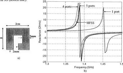
ports.Two
different
one turninductor have been
considered.The first
one with an overalllength
of2
cm and aline
widthof5mm (Fig.
15.a),
and asecondinductor
reducedin
sizeThe
1stinductor
has been
modeled with a2
port and a4
portdivisions in between
segments.
The
results oftheinductance
value shownin Figure 15.b
are compared withHFSS (dotted line).
25
20
15
2cm
1.3
4
ports 4-f'5ports?r
1 porti n
:
n
\ /11
' HFSS / '
- .Z 'I .
-r
A
w
If i i
i i- 1
- - -
-1.35 1.4 1.45
Frequency (GHz)
b)
Fig. J5:a)Single
loop
inductorwithdielectricparameters:d=5u,m,tan(8)=0,e,=4.b)
Inductance VsFrequency
Vsnumber ofPort divisions1.5
It
is clearly
observed that the results are more accurate as the number ofportdivisions
increases. As
the number of portdivisions
is
equal to4,
the segmentation methodperfectly
matchesHFSS
results.As
the width oftheline
decreases,
thenecessary
number of portdivisions
in between
segment might not
be
the same.The
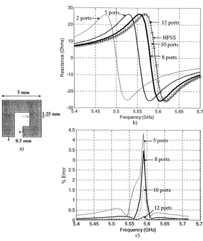
secondinductor
case with aline
width of1.25mm
and a overall size of
5mm is
segmented with adifferent
number of portdivisions
in
between
the adjacent segments.The
results are shownin Figure 16.b
and are comparedagainwith
HFSS (circle
markers).In
that case,12
ports arenecessary
toobtain a perfect [image:39.534.55.476.120.370.2]5mm 5mm ' - UBS : 1 ' > o-< 1.25mm 0.5mm a) LLi 4.5 4 3.5 3 2.5 2 1.5 1 0.5
5.5 5.55 5.6
Frequency (GHz)
b)
I 1 1
j=Sports -i
i t 1 1 1 1 1 1 1 1
fir1 8-ports
l l
1 1
1
t / \-'U
j + 1
) l I i I 1 I t
1 1' \ j 1' \
/ 1' * / /'
~11 //
// ^M
i iu pons
i i
1 '
\
12ports ily -i_______^
5.4 5.45 5.5 5.55 5.6 5.65
Frequency (GHz)
c)
5.7 5.75
Fig.1
6:t
a) Singleloop
inductorwithdielectricparameters:d=5u,m,tan(5)=0,
e,=4.b)
InductanceVsFrequency
for differentnumberofPort divisions [image:40.534.77.486.58.543.2]As
thewidth oftheline
decreases,
moreinterconnect
ports are needed.This
is
causedby
fringing
effectsthat arelarger
whenthewidthis
smaller.a
m
5
Fig
17:Fringing
effects3)
Number
ofGreen's function
eigenmodes:As previously
discussed,
the response of each segmentis
computedindependently
using
the ground/power plane model.For
each segments, theimpedance
matrixis
calculatedwith a
double
summation ontheGreen's function
eigenmodes:-.2 /-2
z>j
=ZZ
i?!ld^2m
c;2,cos(^>,/)cos^j:-)cos^>,;)cos^^)
m^0n=^ab(kxm+k k
)
*sinc
(k
Kyn
K\
9
V z J
sine
(
,
Wn
k^, Isinc XT71 r
V
z Jsine
(
W^
k
-1-xm r\
V z
(33)
The
necessarynumberofGreen's function
eigenmodesin
thex andin
they direction
needs to
be determine in
order to obtain a good convergence of the model.In
thesummation, m representsthem'th eigenmode
in
thex-direction and n representsthen'theigenmode
in
the y-direction.For
this model, m also represents the eigenmode ofthelargest
dimension andis
summedfrom 0
toM
and n represents the eigenmode ofthesmallest
direction
andis
summedfrom 0
toN
asin Figure 27.a. For
the cornerdiscontinuities,
both Green's function
eigenmodesin
the x andy directions
aresummedA 2
turninductor has been
consideredfor
this example(Fig
18.a). The inductor has
anoverall
length
of2cm
awidthline
of2mm
and aspacing
of2mm.
The
segmentationtakesinto
account all the cornerdiscontinuities,
and the number of portsdivision in
between
adjacentsegments
is
setto4
ports.M * y M
\
. a"*
^N
/ XH
--MjHf:
N |-2mm N x10 2cm a) 30 20 10 as -10 1.45 1.5 Frequency (GHz)b)
1.55 -20 -30 ----*=4Shs|
JU
!n
=1!
r
[
;
^
^=5
;
i ' '
"~jj$
r~>~"HF.SS
r i
\j
J7" r i1.4 1.45 1.5
Frequency (GHz)
c)1.55
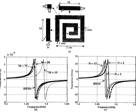
Fig.18: a) Inductor Layoutwithdielectric: d=5^m,
tan(8)=0,
,=4.for different Numberof eigenmodes
b)
withN fixedat 15 c)withMfixed
at75As
shownin Figure 18 b
andc,thesolutionbecomes
closertotheexpected results astrie [image:42.534.43.495.164.535.2]4) Summary
for
SegmentationofRectangular Coils:
The
segmentationneedstobe done
toensurethatdiscontinuity
effects areincluded in
themodel.
The
number ofsegments shouldinclude
onefor every
comerand onefor
eachside.
A
proper segmentationfor
a oneturninductor
is
shownin Figure 1 I.e.
The
number of the portdivisions
in between
adjacent segments needs also tobe
optimized
in function
ofthe width oftheline. It has been
seen thatfor
a width of5mm,
thenumberof
interconnecting
ports requiredis
5,
andfor
a width of1.25,
12
ports wererequiredtoobtain perfect agreement with
HFSS.
Finally,
the convergence also requires a proper numberfor
theGreen's
function
eigenmodes
in
order to obtain accurate results.Convergence
asbeen
seen when thenumber of
Green's function
eigenmodes ofthelargest dimension
was setto75
and the4.3 Circular Coils
Inductor:
43.1
Green's
function forannularSector
cavitiesThe Helmoltz
equation(24)
expressedin
the2-D
cylindrical coordinate systemis
given
in (34):
1
d
(
dG)
1
d2G
pdp{
dp)
p2d<p
1
+k2G=
S(p-p0)5(<p-</>0)
P
(34)
The
termjcopdhas been
removedand willbe
reintroducedlater in
thefinal
solution.The
boundary
conditions require perfect magnetic wall and require that thederivative
ofthe
Green's function
gotozerowith respectto thenormalto theboundary.
Fig.19: Annularsector
For
the annular sector shownin Figure
19,
theboundary
condition gives thefollowing
equation
dG
dp
=
0
(35a)
dG
p=aj>
d(/>
0
(35b)
=0,cr
First,
thesolutionfor
thehomogeneous
differential
equationhas
tobe
obtained:1
d
( dg)
1
d2g
l2 npdp
Vdp)
p2
df
(36)
The
operatorM is defined
asfollow:
MG
=d2G
d</>2
Equation
(33)
becomes (37):
\_d_
pdp
"TpY
M_
\P2
+
k2\g=0
(37)
This
is
aBessel
differential
equation with order -J-M[34],
withthefollowing
solution:g=AJ^(pk)+
BY^(pk)
(38)
J
nand
Yn
representtheBessel
function
ofthefirst
and secondkind.
The
solutionfor
theGreen's function
thatsatisfiestheboundary
conditions(32a)
is
givenby
[34]
a solution ofthehomogeneous
equation exceptat/7-p0
andis
oftheform
of:G
=a<p<p0
Y^(bk)J^(pk)-J^(bk)Y^(pk)
p0<p<b
(39)
The
primefunctions
J
andF
representsthederivative
oftheBessel
function
ofthefirst
and second
kind/n
andF
.The
following
functions
aredefined
tosimplify
thenotations:/
(ak,
pk)
=(ak)Jn
(pk)
-Jn {ak)Yn
(pk)
f(ak,pk)
=Yn(ak)Jn{pk)-Jn{ak)Yn{pk)
(40)
The
following
continuity
conditions must alsobe
satisfied,G\
_=G+
\p=Po \p=Po
dG
dp
P=PodG
dp
P=PoPo
(42)
(43)
To satisfy
(42)
the solutions of(39)
are cross-multiplied and the solutionsfor
thehomogeneous
equation resultin (44):
G
=f^(ak,pk)f^(bk,p0k)
a<p<p0
fjzfi
(bk,
p
k)
fj-f
(ak,
p0
k)
p0<p<b
(44)
Substituting
(44)
into
(43),
we obtain(45):
dG
dp
P=PodG
dp
P=Po2f^(bk,ak)
xp0
To satisfy
(43),
(39)
resultsin (46):
f^(ak,pk)f^(bk,p0k)^S((p-<p0)
G
=2f^(bk,ak)
a<p<pQ<b
fj-^{bk,pk)
f^{ak,p0
k)7c8(<p-<pQ)
2f^(bk,ak)
a<p0<p<b
(45)
(46)
The
greenfunctionis
expressedin
termsofthedifferential
operatorM. The
eigenfunctionBy
[34],
thenormalizedeigenfunctions andtheset ofeigenvaluesare givenin (47):
cos(n
d>)
V
= p-V
p(47a)
{-nl-rt,-n22,...}
(47b)
Where
n pi,I
=nI
a,a
is
thesectorangle, and a =\
p|2p*0
By
[38],
for any
continuousfunction
F(
),
r,^zr* ^v vv 2epfnp(ak,pk)f(ak,p0k)cos(n<p)cos(n<f>0)
(48)
p=o
2fn(bk,ak)
Using
(48)
into
(46),
weobtainthefollowing
Green's function:
_ ^lopf
{ak,pk)f
'(ak,p0k)cos(np<p)cos(np<p0)
f4G(p,HPo^0)=2u
' : ,,,,
v ;
P=o
2fnp(ak,bk)
Unlike
[35],
where a canonly
take afew discrete
valuethat make n aninteger,
in
(49)
there
is
no restriction placed ona.Reintroducing
the jcopdterm,
theGreen's function for
theannular sectoris
givenin
(50):
j
coldly
pfn?
(ak,pk)fnp
(ak,p0
k)cos(np0)cos(np0o)
(50)
(1/7
=0
a<p<p0<k
0<<f><a, 0<<p0<a,
<rp=L
^04.3.2 Impedance Matrix
The impedance
matrixis derived using
(50)
and(23). When
the ports are attheinner
periphery (/?
=a) and the other ports at the outer
periphery
(p
=b),
theimpedance
matrixelements are given
by
[34]:
_
jcopdl
^
Pfnp
(<**>#*)/,,,
(&/c,p^)cos(72^,)sin(pA,.)cos(n^.)sin(7ipA.)^
p=0
fn
(bk,ak)
2A
}P_
KW,"pJ
k denotes
thewave number andis defined
as:k
- co^Jps,Q)
is
the angularfrequency,
fisthe
dielectric
permittivity,p
thepermeabilityandd
theheightofthedielectric.
W.and
W;are
the widths,(/?,,$)
and(/77,0;)arethecoordinates of porti and portj.A. =sin
'W\
K2PiJ
(52)
When p is
equal to zero, the denominator becomes null and the result oftheimpedance
matrix
is
undefined.sinCx)
Knowing
thatlim
=1
, we
multiply
the denominator and numerator of the*-*
x
equation
by
(n
A,)
*(n A
,),
andtheimpedance
matrix whenp
=
0 becomes:
jcop
d I
<7pfn,
(**
Pfrfn,
(bk,
Pjk) cos(/i,4
)
cosfn^
)
%\
2Pi
\(
KW'n,
"A
fnp(bk,ak)
sm(npAj) sin(7tpA,) "A,
A
sin(n
A=)
sin(nA;)
Since,
lim
=lim
=1
p-*> n^. p-o
OpA;
Jij lp=0"
jcopdl
Gpfnyk,pfC)fnp {bktpjk)cos(npfi
)
cos(np0.)
(
2p.&.Y
2/7;Ay./
(**,**)
vw;
jvw;
y(54)
4.3.3 Considerations for
convergenceissues
foranalytical modelFirst,
thecoil needs tobe
generated.Circular inductors
canbe
segmentedwith semicircles as shown
in Figure
20. Each
mm canbe
segmented with2
semi-circles.The
radiusofeach new semi-circle
is incremented
by
thespacing between
themetallines.
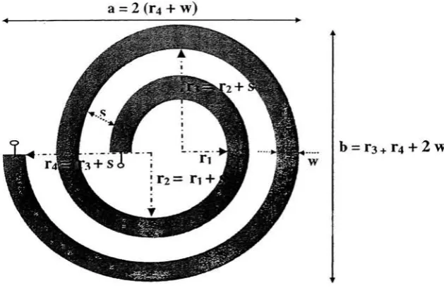
a=2
(r4
+w)b=T3
[image:49.534.140.455.371.575.2]+T4+
2
WAs previously discussed for
the rectangular coils,different
variables need also anoptimization
for
circular coils, such as the number of segments, the number of portsneeded and the number of
Green's function
eigenmodes.This
sectioninvestigates
thevalue ofthese
different
varia