Rochester Institute of Technology
RIT Scholar Works
Theses
Thesis/Dissertation Collections
5-1-1986
PMOS digital structures
Robert Pearson
Follow this and additional works at:
http://scholarworks.rit.edu/theses
This Thesis is brought to you for free and open access by the Thesis/Dissertation Collections at RIT Scholar Works. It has been accepted for inclusion
in Theses by an authorized administrator of RIT Scholar Works. For more information, please contact
Recommended Citation
PMOS DIGITAL STRUCTURES
by
Robert Pearson
A Thesis Submitted
in Partial Fulfillment of the
Requirements for the Degree of
MASTER OF SCIENCE
in
Electrical Engineering
Approved by:
Prof.
Renan Turkman
-=--~----~~----~-=~-.--~-.----Dr. Renan Turkman
(Thesis Advisor
Pro f .
--=--__
R=-o-=g~e--=-:r:__E,...._e
.,.-H
__
e--,-i
---"n __
tz----;-:--:---:--_
Dr. Roger Heintz
(Committee
Prof.
---=--J---:o:---::h_n-==-:-L
e-;--E_I""",,,:""1i
S~--:-:-:---:,.---_
Dr. John Ellis
(Committee)
Prof.
Swaminathan Madhu
-=D-r~.~S~w-a~m~i·n-a~t~h-a~n-7M~a~d~h-u----~~--~---( Department Head )
DEPARTMENT OF ELECTRICAL ENGINEERING
COLLEGE OF ENGINEERING
ROCHESTER INSTITUTE OF TECHNOLOGY
ROCHESTER, NEW YORK
MAY, 1986
Permission to Reproduce
Title
:
PMOS DIGITAL STRUCTURES
PREFACE
The purpose of
this
workis
to create a total package ofinformation
aboutthe
RIT pMOSFET fabrication process. Thispaper should
then
serve as a student referencein
coursesin
both
the
Electrical and MicroelectronicEngineering
departments.
The material presented should alsobe
of use tostudents
in
the
Computerengineering department's
VLSIdesign
course who wish
to
actually
fabricate
theirdesigns.
Theresults presented
in
this paper were obtainedfrom
two pMOSmask sets
both
of whichhave
subsequently
been usedin
Electrical and Microelectronics courses. This
demonstrates
that
the pMOS processhas
reached a maturelevel
andis
nowwell enough
defined
sothat
first
timeprocessing
people suchas EEEE 676 students can expect
their
own circuitdesigns
to
work after fabrication.
This work was made possible
through
the
assistance ofthe
many
peoplein
the
MicroelectronicEngineering department,
in
particular Dr. Lynn Fuller and Dr. Renan Turkman. Dr. John
Ellis of
the
ComputerEngineering
andComputer
Science departments served asthe
source ofthe
originalinformation
on the design rulechecking
software Lyra.PMOS DIGITAL STRUCTURES
by
Robert E. Pearson
Rochester Institute of
Technology
Microelectronic
Engineering
DepartmentRochester,
New YorkABSTRACT
A
majority
of newintegrated
circuitdesigns
arebeing
fabricated
in
CMOStechnology
which usesboth
pMOSFETs andnMOSFETS. The nMOSFETS have
been
well characterized over thepast
few
years whereasthe
pMOSFETshave been
ignored
sinceMOS
technology
movedto
nMOSin
theearly
70 's.Investigation
of pMOS devices will provide
information
that willbe
usefulfor
other technologies such as CMOS. This paperlooks
at thedesign,
fabrication,
fabrication
simulation,
electricalcharacterization, electrical simulation and
testing
ofdigital
pMOSFET circuits. A particular emphasis will
be
placed onunderstanding
the
process sothat
firsttime
integrated
PMOS
DIGITAL
STRUCTURES
TABLE OF CONTENTS
PAGE
NUMBER1.0
INTRODUCTION
1
2
.0
PMOS
ENHANCEMENT
MODE
FETS
4
2
.1
BASIC
STRUCTURE
4
2.2
DESIGN
RULES
132.3
SPICE PARAMETER EXTRACTION
24
2.4
THE
BODY
EFFECT
393
.0
FABRICATION
43
3.1
SIMULATION
USING
SUPREM
433
.2
USE
OF
CONTROL
WAFERS
52
3
.3
FABRICATION
PROBLEMS
644
.0
LAYOUT
OF THE FABRICATED CIRCUITS
70
5.0
CIRCUIT AND DEVICE RESULTS
775.1
INVERTER
DESIGN
775.2
LOGIC
LEVELS
ANDNOISE
MARGINS 875.3
RING OSCILLATOR 935.4
PASS TRANSISTORS 995.5
SHIFTREGISTERS
104
5.6
LOGIC
FUNCTIONS
108
NOR GATES NAND
GATES
6.0
CONCLUSIONS
BIBLIOGRAPHY
APPENDICES
APPENDIX
A-APPENDIX
B
-APPENDIX
C-APPENDIX
D
APPENDIX E
APPENDIX
F
APPENDIX
G APPENDIXH
Process cross-sections
Partial
Lyra
symbolic rulesetPrograml
listing
for SPICEparameter extraction
Completed
process sheets SUPREM resultsProgram
VINOUTlisting
SPICE
program listingsICE
Intearated Circuit Editorfiles
PAGE
NUMEER123
1.0
INTRODUCTION
The
purpose of this work is to create a total package ofinformation about the
RIT
pMOSFET fabrication process. Thiswill include a set of
design
rules for a Computer Aided Design(CAD) system, as well a completed fabrication worksheet. The
simulation of the
fabrication
process results using theprocess simulator SUPREM will be described. SUPREM stands for
Stanford
University
PRocessEngineering
Models program.The
test results on a number of circuits will be presented along
with the results predicated
by
the circuit analysis programSPICE.
The
method ofextracting
the model parameters for usein SPICE will also
be
included. Some of the fabricationproblems will be discussed in relation to their elimination
for better process flow and repeatability. This paper should
then serve as a student reference in courses in both the
Electrical and Microelectronic
Engineering
departments. Thematerial presented should also be of use to students in the
Computer engineering department's VLSI design course who wish
to actually fabricate their designs.
Once
the ramifications of different design choices havebeen explored devices can be fabricated.
Testing
of thedevices will show the degree of agreement between our design
rule based predictions and the actual results. The guidelines
can be modified if inaccurate, or process variations can be
examined. The end result will be a set of device (circuit)
design rules, a set of layout rules and a process which if
digital circuit.
The
characterization of thedc
parameters of the test structuresindicates
the limits on circuit andprocess parameters compared to the simulated performance. The
characterization of the speed capabilities of basic circuit
elements
(inverters)
through
the use of a ring oscillator willallow
future
designers
to estimate the maximumfrequency
of operation of more complex circuits.The results presented in this paper were obtained from
two pMOS mask sets both of which have subsequently been used
in Electrical and
Microelectronics
courses. The first maskset was
layed
outby
hand on mylar grid paper and the 200x artwork cutby
hand into amasking
film called rubylith foreach of the four layers. A complete set of four lOx reticles
were then produced
by
photo-reduction.The
four working lx emulsion masks were thenphoto-repeated from the reticles.
The fabrication was then done
during
non-laboratory
hours in the microelectronics laboratories.The second mask set layout was done on a GiGi terminal
connected to the VAX 11-780 running a layout program called
ICE
developed at RITby
Taylor Hogan.The
software generateda file that could be read
by
the pattern generator to create areticle
directly
without the use of rubylith. The file first had to be put onto paper tape to be readby
the patterngenerator. Once the reticle was produced the process for
generating the working masks was the same. The purchase of an
HP-7580B plotter now allows the designer to have large size
that CAD tools
have
been
used here at RIT todesign,
lay
out.and
fabricate
masksfor
a pMOS circuit. The second mask setwas
designed
andfabricated
as part of a weekly demonstrationfor EEEE
670
Introduction
to Microelectronics. The studentsin this class were required to do circuit layouts although
their
designs
were not include on the second mask set. Itwill be easy for these students to create a pMOS mask set as
part of
EEEE
676Integrated
CircuitProcessing
sincethey
already have some
layout
experience. Fabricationby
thesestudents leads to the requirement of a stable pMOS process,
which is the major point of this paper.
During
the quarterthat the
fabrication
of the demonstration took place the workwas intermittent and not a great deal of care was taken in the
processing. In spite of the lack of attention to process
details the results were quite good and in line with the
expected results. This demonstrates that the pMOS process has
reached a mature level and is now well enough defined so that first time processing people such as l-iKHfc 676 students can
expect their own circuit designs to work after fabrication. A further proof of the increased control of the pMOS process is
the successful fabrication of circuits
during
the one weekshort courses offered
by
the MicroelectronicEngineering
department. These circuits were processed for the most part
by
complete novices and produced working circuits.
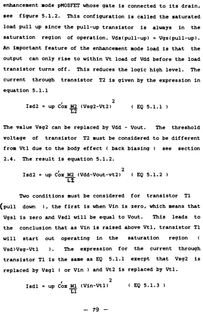
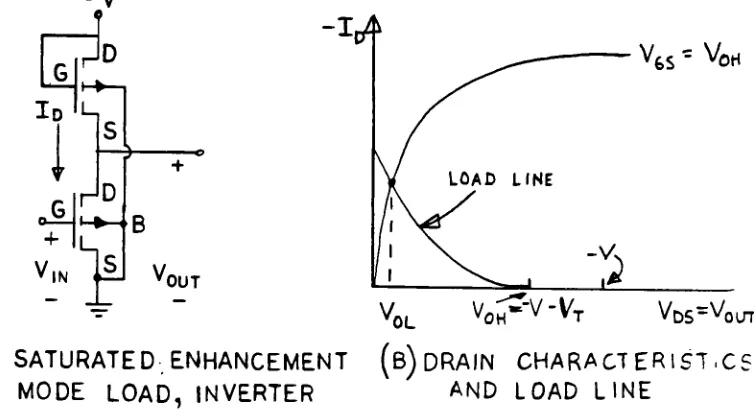
2.0
PMOS
ENHANCEMENT
MODE FIELD EFFECT
TRANSISTORS2.1
BASIC
STRUCTURE
The
basic
elementin
the
fabricated
chip
setsis
thep-channel enhancement node metal oxide semiconductor
field
effecttransistor
(pMOSFET)
whose cross-sectional structure isshown in
figure
2.1.1.
A
moredetailed
set of cross-sectional views canbe
found
in
appendixA.
The
sourceis
the terminal where the charge carriers,holes
in
this
case,have
thehighest
potential and thedrain
is
thelower
potentialterminal
the
carriers flow to.In
the circuits tobe
described
later
the highest
potential willbe
ground and thelowest
possible potential willbe
thesupply
voltage minusVdd.
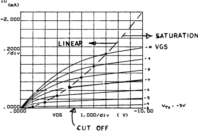
The
pMOSFET structurehas
atypical
current vs. voltage(I-V) characteristic shown
in
figure
2.1.2.
The
mostimportant
aspects of the characteristic arethe
three regionsof operation of
the
pMOSFET.The
first
isthe
cutoff regionwhere no
drain
to source currentflows
(Vds
<Vthreshold)
.The
threshold voltagefor
a pMOSFET canbe
defined in a numberof different ways.
The
measurement ofthreshold
voltages will bediscussed
in
moredetail
in
the
SPICE
parameter extractionsection.
The
second region isthe
linear
region where thecurrent flow is influenced
by
both
the
drain
to source voltage and the gate to source voltage (Vds < Vgs-Vt).The
thirdregion is the saturation region where the
drain
to sourceSOURCE CAT! I ? UL
BULK (-jik
afib)
Figure
2.1.1
-pMOSFET cross-sectional structure
?
SATURATION
VGS
OOOOl^Sd
.0000
T
VTe
"*vVDS
|
1.000/div C V)CUT
OFF
Figure
2.1.2
-Typical
pMOSFETI-V
characteristic-sfcowing
the cutoff, linear and saturation regions [image:12.509.131.460.309.531.2]-approximation of a
pMOSFET,
higher level models will bediscussed
and applied at appropriate timeslater
in
thispaper.
The
equationsdescribing
the relationshipsin
thevarious regions will
be
presented in section5.0.
The
voltagesubscripts
have been
adoptedto
correspond tothe
negativesupply
voltageVdd,
so thatVds
is negative asis
Vgs.
The
fourth device
terminal
shownin
figure2.1.1,
thebulk
or substrate connection has an inportant effect on thepMOSFET I-V characteristic,
especially
the threshold voltage.When an enhancement mode pMOSFET has
its
source and substratetied
to
groundit
has a threshold voltage thatis
called Vto.If
the source is allowed to take on voltages differentfrom
the substrate (Vsource to
bulk
=0)
then the threshold voltageof the
device
will change.It
is this change in thresholdvoltage with source to bulk
biasing
which is called the backbiasing
orbody
effect.The
body
effect makesdesigning
anall enhancement mode transistor circuit more difficult than
some other types of circuits.
As
an example consider thecircuit shown in
figure
2.1.3.
If
weignore
thebody
effectVout
wouldbe Vdd-Vto but
sinceVsl
is
not at groundthe
body
effect causes Vtl to be greater than
Vto
andVout
is
less thanexpected.
A
plot of thebody
effect vs.Vsb
can befound
insection
2.4.
The relationship
between
the
device
cross-sectionalstructure and the
I-V
characteristics is affectedby
thephysical layout of the regions of
the
structure.A
top
viewV=
-10Volts
Vin= -5
Volts*-_ Vti
4
Vto<= BODY EFFECT
. since Vsei =Vout TO-* *
U"
G2
VouT
L^JWLK
Vt2.
Vt0 =^> .3V()LTt
I s?
~
SINCE VSB2=0
Figure
2.1.3
-The
body
effect on threshold voltage fortransistors with different source to bulk
voltages
<*
-t>
X
SOURCE GATE DRAIN
diffusion
(ice-green)
thin oxide(ice-red) contact cuts
(ice-white) METAL
(ICE-LUE)
Figure
2.1.4 - Compositetop
view of a pMOSFET-x and
y dimensions
ofthe
pMOSFET layout.The
layer
names andcolors correspond
to
the
correct processfile
for
pMOS whenusing the
Integrated Circuit Editor
(ICE) program. Certainrules which must
be
followed
were usedin
laying
out thepMOSFET shown.
Designs
which contain just a few suchtransistors
canbe
visually
checkedby
the designerfor
compliance to
the
rules.Some
common process problemsinvolving
thedesign
rules are illustrated in figure 2.1.5.The
design
rules used in this work are;Minimum
diffusion
todiffusion
spacing
Sdd
Minimum metal to metal spacing
Minimum contact cut
to
contact cutspacing
Minimum
diffusion
width Minimum metal widthMinimum contact cut width Minimum thin oxide cut width
Sdd
= 10 micronsSmm
= 10 micronsSec =
30
micronsWd =
30
microns Wm =30
microns Wc = 10 micronsWt
= 10 micronsEdc
= 10 micronsEtc = 10 microns
Emc
= 10 micronsIt
= 10 microns Minimum diffusion extension beyonda contact cut
Minimum thin oxide extension beyond
a contact cut
Minimum metal extension beyond a
contact cut
Minimum thin oxide indent
Probably
the most criticaldesign
ruleis
the choice ofthe minimum drain to source diffusion
spacing
(seeSdd
above).Figure 2.1.6 shows that
if
the maskdimension
Mdis
too smallthe result might be that no region
is
availiable in which toenhance a channel, the
drain
is
already
shorted to the source.One of the parameters
that
influences the choice of theminimum mask dimension is the power supply voltage Vdd.
The
"C
J
LATERAL DIFFUSION
CAUSES
A SHORT
Diffusion
spacing
too close drain and source shorti
I
LEFT
-Missalignment
of the thin oxide mask does notchange the channel width due to the
indentations
RIGHT
-Incorrect
desicrn
rule causes channel width chanaeINCOMPLETE
CHANNEL
LEFT
-Metal extension over diffusion allows missalignment
RIGHT - Metal too narrow to ensure a complete channel
Figure
2.1.5-Process problems related to
design
rules-i
SOURCE DIFFUSION Xl
l^i
TJ"1
/T
I
-i
_!_L>*^./$
>^
vl!l
-t _
CHANNEL LENGTH
MD
DRAIN DIFFUSION
BULK
N-TVPEDIFFUSION MASK SPACING
U-AL*
~*\'l~*i+*i
r4-Vw
*-in-'/wg
\
AL,
W,
ALd=%tan
t
tanetf
L
=MD-ALS-AL
logic
levels
are availiablealong
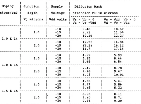
with their noise margins.The
choice ofsupply
voltage affects the depletionlayer
widthassociated with
the
drain
and source diffusions.Using
alarger
supply
voltage gives wider noise margins and morewidely
separatedlogic
levels
but requires one of thejunctions
be
ableto
stand off a larger reverse bias.As
thereverse
bias
increases
the
depletion
layer width increases andthis
wouldincrease
the spacing necessary to obtain aneffective channel.
Table
2.1.1
shows some of the calculationsof minimum
diffusion
mask spacing Mdfor
various values ofsupply
voltage.The
valuesin
the table are the spacing forzero channel
length.
The
depletion
layer
widths canbe
madesmaller
by
choosing
a moreheavily
doped substrate. Thiswould reduce the spacing,
but
the higherdoping
level
wouldincrease the threshold voltage necessitating an increase in
the
supply
voltage to achieve thedesired
logic
levels.The
higher
supply
voltage would in turn increase the depletionwidth thus negating
any
gains.Twelve
microns was chosen forMd
on the first chipfabricated,
partly
due to thehand
layout
using Rubylith. The second
chip
wasfabricated
using an Md often microns.
A
computer program calledDSPACE
was written togenerate the data shown in
table
2.1.1.
A test
chip
withdrain to source diffusion spacings
down
totwo
or threemicrons is currently
being
fabricated
totest
some ofthese
findings.
The
testchip
has
drain
and sourcediffusion
junction depths of under one micron.
[image:18.509.54.457.47.574.2]-Table
2.1.1
Proaram DSPACE
resultsDoping
atoms/cm3
Junction
depth
Xj
micronsSupply
Voltage
Vdd
voltsDiffusion
Ma dimension MD sk in micronsVs
= Vd =Vb
= 0Vg
=VddVs Vd
= Vdd Vb = 0
=
Vg
= Vddi n v ia.
-1.0
-10 -15 -20 9.46 9.91 10.26 10.67 11.56 12.272.0
-10 -15 -20 12.55 13.19 13.7 14.84 16.12 17.141 ft F 1; .
1.0
-10 -15 -20 4.995.25
5.45
5.93
6.44 fo.841 U C 13 "
2.0 -10 -15 -20
7.42
7.76 8.038.78
9.4/ 10.01 1.0 -10 -15 -20 4.55 4.77 4.955.41
5. 86 6.221.5 C 13 "
[image:19.509.22.487.120.463.2]2.2 DESIGN RULES
The
list
ofdesign
rulesalready
providedis
not completeenough
to
allow someoneusing
only
these ruleto
fabricate acorrect
working
transistor.
Additional
rules such as theindentation
of thethin
oxide cuts todefine
the channel widthmust
be
specifiedin
a more abstract way, such asby
diagramsshowing
variations on correctlayouts.
Obviously
this type ofdesign
rule specification andchecking
would becometo
cumbersome
for
circuitscontaining many
transistors. Softwareknown
asdesign
rule checkers can take a design which isstored in a computer
file
as a series oflayers
ofboxes
andcheck it
for
compliance,reporting
thelocation
and nature ofany
errors.The
design
rules checkedby
the computer must bevery
complete or the user would still be left to check certainareas or rules
by
hand
which would defeat the purpose of theautomated checker.
The
following
paragraphsdescribe
the methodby
which theRIT
four
level
metal gate pMOS designrules can be specified for a particular
design
rulechecking
program called Lyra.
For
a completedescription
of how tospecify
design rulesfor
Lyra
seebibliography
referencenumber one.
The
fabrication sequencedescribed
in
appendixA
requiresfour masks; the
diffusion
mask,the
thin oxide mask, thecontact cut mask and the metal mask.
A
symbolic rulesetspecification will
be
developed
for
use with theLyra
layout
rule checker.
Each
rule gives a context (type of corner and layer) whereit
applies, and a set of constraintsto be
13-applied at
these
corners.The
rulesetfor
this process willbe
called pmosRIT.r(
See
appendixB
).
The
organization ofthe
rulesetfile
is
asfollows;
1)
primary
layer
specification2)
compositelayer
specification3)
rule constructs and rule macrosThe
primary
layers
specification has thefollowing
form;
(primary-layers
(D(diffusion PDIFF) )
(T(thinoxide
POXIDE) )
(C(cuts
PCO)
(M(metal
PMETAL)))
The
single characterlabel
is
for
internal use(
within theruleset ) and
the
nextlabel
is
for
useby
thelayout
programCaesar,
while thelast
label
is
the Cal. Tech.Intermediate
Format
(
CIF
)
layer.
A
technology
file
mustbe
createdfor
Caesar
todescribe
the layers in the pMOS process.The
P
infront
of the CIFlabel
is
used toidentify
thelayers
asbeing
for the pMOS process.
At this point we can
define
lambda
as the minimumalignment
tolerence,
which we will considerto be
5
microns.Using
this definition the minimum line width or extensionshould be two lambda or
10
microns.If
lambda
is used as theminimum line width, other
design
rulechecking
software whichuses half widths would
have
todeal
withfractions
of lambda.To
avoid thislambda
is
chosento
be
small enough so thatintegral multiples of
lambda
canbe
used.Lyra
only
looks
ata problem
for
Lyra to deal
with fractions of lambda.The
next section ofthe
rulesetfile
is
for
thespecification of composite
layers,
but first we will write arule
for
anindividual
layer.
After
this example it willbe
easier to understand the need
for
composite layers.The
rulethat
we want tospecify
to
the
Lyralayout
rule checker isthat
the
diffusion
regions must be at least three lambda wide.The
format
for
this
rule macro in the ruleset is givenbelow;
(width
D
6 "D_W")
Where
D
refers todiffusion,
the 6 gives the number ofhalf
lambdas
wide thediffusion
shouldbe
( 30 microns)
, and theMD_W"
is the error message that
is
reported if the rule isviolated.
This
macro can be expanded to the exact rulespecification.
For
rulesinvloving
two or more layers it isnot
likley
that there will be anexisting
macro to use and acomplete rule specification will be necessary.
The
completerule specification for this macro
is;
(rule
(corner:(a
D) )
(constraints :
( inside
6 D
"D_W") )
)(rule
(corner:(o
D) )
(constraints :(e-inside 6 D "D_W" ) ) )
The a refers to an acute corner and
the
o to an obtuse corneras shown in
figure
2.2.1
(a).Inside
and e-inside are calledconstraint macros, also specified
is
thatthe
diffusion be
sixhalf lambdas wide.
-ACUTE ANGLE a
V///A
/
FEATURE/
/
/
XOBTUSE
ANGLE
V
a-(A)
THE
TWO
CORNER
TYPES
(b)
QUADRANT
NUMBERING
-ACUTE
V
OBTUSE %o'tc)
CANONICAL
CORNER
ORIENTATION
Figure
2.2.1The
constraint macroinside
canbe
expanded to show howthe
layout
checker uses cornersto
evaluate compliance to thedesign
rules.;
Equivalent
of theinside
constraint macro(Build
constraint: (Quadl6
6)D
"D_W")
In
this
statementthe
constraint is thatin
quadrant one ( seethe quadrant
numbering
scheme in figure 2.2.1(b)
) theD
orPDIFF
layer
be
found,
and that it be at least sixhalf
lambdason a side.
The
other constraint macros are illustrated inFigure
2.2.2,
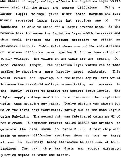
some of which will be used later.Some
ofthe
other single layer rule macros are listedbelow (
NOTE:
These
haveimplied
constraint macros withinthem
)
;(ss
D
4"D_s")
; minimum diffusion to diffusion spacing (widthT
4 "T_W") ; minimum thin oxide width
(width C 4 "C_W"
) ; minimum contact cut width
(ss
C
4 "C_s") ; minimum contact cut to contact cutspacing
(width M 12
"M_W")
; minimum metal width(ss M 4 "M_s") ; minimum metal to metal spacing
The next level of
compexity
in
rule specificationinvolves the extension the
diffusion,
thin oxide and metallayers around a contact cut.
The
contact cut is used to makecontact between the
diffusion
and the metal soboth
of these layers must extend beyondthe
cut,but
the
cut should alsobe
made through the thin oxide so the thin oxide must extend
beyond the cut layer as well.
A
fictional
compositelayer
called
E
consisting of the presence ofdiffusion,
thin
oxideand metal can be created
in
the
compositelayer
specificationsection as shown below.
[image:24.509.33.454.133.604.2]-CL
n
t
INSIDE
IS A LAYER INSIDEA CANONICALLY
_.DRIENTED CORNER
V
OUTSIDEIS A LAYER OUTSIDE A CANONICALLY
ORIENTED CORNER
Q
E-INSIDE
DOESA LAYER INSIDE A CORNER
EXTEND INTO QUADRANTS 2 AND4
JY AN AMOUNT X
E-OUTSIDE
DOESA LAYER OUTSIDE A CORNER
EXTEND JStO JJUADRANTS 2 AND 4
BY AN AMOUNT X
i
S-INSIDE
ISA LAYER INSIDE A CORNERSPACED X AWAY FROM ANOTHER
FEATURE IN THE SAME LAYER
D
S-OUTSIDE
IS A LAYER OUTSIDE A CORNER
SPACED X AWAY FROM ANOTHER
FEATURE IN THE SAME LAYER
;composite
layer
specification(
composite-layers(
E
(
andD T M
) ) )
;E
for extensionThe
contact cut rule canthen be
specified relative to thecomposite
layer
E.The
contact cut rule(actually
many
rules)specification
has
the
following
form.;diffusion
thin
oxide and metal extension beyond contact cuts(rule
(corner:
(aC) )
(constraints: (e-inside
2
E "C_x")
)
)(rule
(corner:
(aC) )
(constraints:
(e-outside2
E
"C_x") ) ) (rule
(corner:
(oC) )
(constraints: (e-inside
2
E
"C_x")))
(rule(corner: (o
C) )
(constraints: (e-outside
2
E
"C_x")))
Note
that
to check both acute and obtuse angles two rules arerequired, e-inside and e-outside, this to make sure that the
cut is
completely
surroundedby
theE
composite layer.A
design rule problem area is the indentation of the thinoxide
to
define the active channel width.The
indentation
causes the need to
handle
acute and obtuse anglesdifferently
as shown
in
figure2.2.3.
The
thin
oxide cutlevel
mustbe
aligned to both the diffusion and the metal
levels
on theacute corners but on
the
obtuse corners there must bediffusion in all four quadrants and
thin
oxidein
only
three.
To further explain the rule
definition
process theexample layout in figure
2.2.4
willbe
used.We
aretrying
toget the rule checker to
determine
if
layer
B
is
on or within
-OBTUSE
-DIFFUSION MUST SURROUND
THE CORNER
INDENT -DEFINESCHANNEL WIDTH W ACUTE
REQUIRES A DIFFERENT RULE
DIFFUSION THIN OXIDE
Figure
2.2.3
-Thin
oxideindentation
and obtuse anglesLAYER B
CORNER ANGLE
1 ACUTE
2 OBTUSE
3 ACUTE
4 ACUTE
5 ACUTE
6 ACUTE
Y/A
LAYER A c>5C3 layer bFigure
2.2.4layer
A
on all sides.Starting
at corner1,
if
the insidemacro
is
usedto
seeif
B
is
inside ofA
we can startby
rotating
the
images
into canonical orientation(see
figure2.2.1
(c).Figure
2.2.5
shows the result andit
canbe
seenthat
at corner1
oflayer
B
it
isinside
ofA.
For
corner2
rotated
to
canonical orientation as shownin
figure 2.2.6 wefind
that
thedesign
rule checker would say that corner2
oflayer
B
is
inside
of A and would not see the problem inquadrant
II.
A
different or additional macro should be used to checkfor
thepossibility
of this condition occuring.It
can
be
seen that the results for corners3
and4
are the sameas
for
corner1.
For
corner number5
we find that an errorhas
occured and corner 5 of layerB
is is not inside of layerA (see figure 2.2.7).
Finally
for
corner6
wefind
that it isinside
oflayer
A.
If
the macro e-inside is used on cornernumber
2
as shownin figure
2.2.8 wefind
that thepreviously
undetected error has been found.
The partial ruleset file pmosRIT.r can
be
found
in
appendix B.
A
revised rulesetreflecting
the projected improvedlithography
and alignment capabilities willbe
generated as necessary.
Layout
of a pMOSdigital
chip
should be done using thelayout
capabilties of the computerengineering department
(
Caesar)
in orderto
checkthe
validity of the these rulesets.
By
using
these otherlayout
systems we can also check
to
make sure that the generatedCIF
files canbe
used withICE
to generateMANN
files
for
thepattern generator.
-CORNER I ROTATED TO CANONICAL
ORIENTATION
INSIDE MACRO
VIEWING WINDOW
Figure
2.2.5-Corner
number J rotated to canonical orientationexamined usincy the inside macro rule
CORNER 2 IN
CANONICAL ORIENTATION
PROBLEM
NOT
DETECTED
A BUT NO B
remember figure
is rotated
Figure
2.2.6
-Corner
number2.
rotatedto
canonical orientation
CORNER
5
ERROR
LAYER
A
MISSING
Figure
2.2.7
-Corner
number 5. rotated
to
canonical orientationexamined usincr the inside macro rule
CORNER 2 IN
ERROR
DETECT
E-INSIDE MACRO
VIEWING WINDOW
Figure
2.2.8
-Corner
number2,
rotated to canonical orientationexamined usina the e-incide macro rule
2.3
SPICE
SIMULATION OF PMOS DIGITAL
STRUCTURESTo design
anintegrated
circuitusing
the pMOSFET alreadydescribed
it
is
necessary
to create a model of the electricalbehavior
of these transistors and then usethe
model topredict
the
behavior
ofthe
circuit.Since
there are somany
transistors
in
atypical
circuithand
calculations are out ofthe question and a computer analysis tool is required.
In
theextreme case such as a
very
large scale integrated (VLSI)circuit not even a computer analysis tool can do the job.
The
computer analysis
is
done
on small cells and the cells joinedtogether to form the
finished
circuit. The circuit analysisprogram used in this work is SPICE version
2G
running on theDEC
VAX
11-780
VMS computers at RIT. SPICE will be usedthroughout the analysis of the various circuit structures on
the chips.
By
changing
the transistor model parameters andkeeping
the same circuit we can predict the effect of process
parameter variations on the circuit's electrical performance.
The
truedevice
design workis
in
deciding
what the physicaldevice parameters should be
for
optimumdevice
performance.The ability of the
designed
circuit to withstand processvariations is a good
indication
of how successfullthe
derived
design and process rules are.
It
isbeyond
the
scope of thisproject to investigate process variation effects on circuit
performance, so the spice model parameters presented will
be
been
extractedfrom
previously
fabricated pMOSFETs. Figure2.3.1
shows a cross-section of a pMOSMET with all of theelements
included
that are necessary to model thedevice
forSPICE.
There
are41
parametersin
the spice model, some ofwhich are not
necessary
for
the
level one model (30-41 shortchannel and noise effects).
The
short channel parameters willbe
important
for
future shallow junctionfive
micron spaceddiffusion
pMOSFETs.Many
of the remaining parameters arecalculated from the basic device parameters such as gate oxide
thickness
and substrate doping.A
set ofSPICE
parameters that are valid at a particularset of
Vds
,Vgs
and Ids values can be extractedby
handcalculation using known processing information.
For
the pointVds = -6V
,
Vgs
= -9v andIds
=-880uA (see
figure
2.3.2) wewill extract
SPICE
parameters. Note that the point that wehave chosen is on the edge of the saturation region (Vds = Vgs
-Vto where Vto = -3V, see
figure
2.3.3
for
Vto).
From
theprocessing we can state that TOX = 700
Angstroms,
NSUB =1E15,
TPG =
0
(aluminum),
XJ =2
microns andLD
=1.5
microns.The
area and the perimeter of the source and
drain
should also beknown,
these values caneasily
be changedfor
different
sizetransistors.
For
this transistor the perimeter of the sourceand drain is
200
microns and the areais
2500
square microns.SPICE uses many parameters that are per unit area or per unit
perimeter and can therefore calculate the actual value
for
different size transistors.
The
first
parameterthat
willbe
derived is
Lambda,
the channellength
modulation parameter.
-SOURCE
S
METAL
CGSO=t
d=T2=:
GATE
G
_L
EACH
METAL
A
DRAIN
D
=^CGDO
T\
METAL
Si02
)
^P-TYPE
CBS
--VW-Rn
P-TYPEs
CGBO
=j=CBD
I N TYPE BULK
B
BULK
m . x * -u
I
~ L .0 0l
a l D_a. -w c o o l a- > *4 8>jwwn >
*i a a (0 (0 u o a L i i 0 LU LU *> m CD c in 0) T m (0 > i 1
P a a a a Q o 0 + + L LU LU 0 t^ m 4* m c r> CM T* -i CM X
CO co D o a + + < LU LU a: ro Q a N a f\l .-* in (T)
(0 (0 o o a LU LU < CO m or u CQ .-H
wH m
tH (\l LU LU Z z ^^ N-1
_l _l (X iH u 1-1 Eh l. N m CM (D
-S>> a a aaa oo o o o-.
go a a a a o a oao
i\iin a. 1 i i
N ?
WU I
L x
0*> J) l 0.0. an c o o a -d LU*>>> LOT o>_iwww 6> > > 5
6
a * baa ou w w
ifi
*> i5
C 0) 0 > u m >3 HI
*
*>
*
o
_JQ_
U HHQ.tt:
*
*
*
*
*
a:* a co *M o oJcn en a cTo o o 0 L 0 c > jl i LU o CD .-1 i LU 0) 1 3= #"N"*vT^
iri i > SNN^
_^, vxvL
N|
^
^
> J: o + 3 t pja VX
^
LU CO
JJ
1
LU
^
. NOQ O
0) CM
m
-I nt- !S<N
a
N
^
\ a m XI
or CO 0 o + LU CO COri
o o + LU in (0N
^
> .1 o a o^
U) > 1 1 i m o m o a: a i LU i LULU < in CO
>c 0) o
cc
< L0 (0
3: a
o o
1 1
om O > c -t CM
do a . III llJ
. 1 OTJ OCM 7 7.
olu .\ a i I-H
^1 H
Lambda
is
givenby
the slope of theIds
vs.Vds
curve at thegiven point,
in
this
casethe HP
4145 parameter analyzer wasused
to draw
atangent
to
the curve at the point and the slopeis
displayed
in
the
legend box
below the plot.Lambda
=Q
Ids
= -31.3X10-6 = 0.03557 1/voltsEQ
(2.3.1)/
Vds
(Ids) -880X10-6The
next parameter to be calculatedis
KP,
thetransconductance.
The
equationfor
the drain to sourcecurrent
is
givenby:
2
Ids
= KPW
(Vers-Vto) (1+Lambda|
Vds|
)EQ
(2.3.2) 2L
Solving
for
KP
yields L mask-2
LDKP = 2
L
Ids
=2 (10-2(1.5))-880X10-6
2
2W (Vgs-Vto) ( 1+Lambda
|
Vds|
) 30C-9-3) ( 1+0. 03557(|
-6|
)KP =
9.401X10⁻⁶
The oxide capacitance per cm2 is calculated using
Cox' =
ErSi02(Eo)
=(3.9)8.85X10-14 = 4.9307X10⁻⁸ FEQ
(2.3.3)TOX
700X10-8
cm2The mobility UO is
KP/Cox'
= 190.66 cm2/V-sec.
Gamma,
thebulk threshold parameter is calculated by:
Gamma =
(l/Cox')(^2q
ErSi02
Eo
NSUB ) = 0.369EQ
(2.3.4)which can be used to calculate the actual threshold voltage
Vt =
Vto
+Gamma|J|-2<f
+Vsb|
-HM\
EQ
(2.3.5)Using
the actual threshold voltages another set of values forgamma can
be
found.
The
valuesfor
gamma calculated in thismanner are .341 at
Vsb
=2V,
.18 atVsb
=4V.
.12 at Vsb = 6V. This shows a greaterdeviation
atlarger Vsb
values. The zero-bias
threshold
voltage can yield the amount of surface statesby
solving
thefollowing
equationfor
Nss:Vto
=0ms
-aNss
-2/f
-2 i/aErSi
Eo
NSUB^frfEQ
(2.3.6)Cox
'Cox
'Nss
=Cox
'1
-q
[-Vto
+ jdms-20f
-2VgErSi Eo NSUBjf
Cox'
J
Nss
=5.409X10+11
The
drain
and source series resistance can be calculated usingpreviously
measured sheet resistance, the contact resistanceand the
length
to width ratio of thedrain
or source (seefigure
2.1.4).
Rd
= Rs = R + ReEQ
(2.3.7)Rd =
(Rsh)Ldiff
+ l/(sqaure microns of contact area) ( 1. 24X10-4)
Wdiff
R = 17
(30^
+1/(300X1.24X10-4
ohms/micron2) = 37 ohms^
The
capacitances used in the SPICE model are calculated fromcapacitance per unit area or capacitance per unit
length
andcan
easily
be
found
for
different
size transistors.The
junction capacitance per unit area is
found
by;
CJ =
((ErSiHEo)
)/WEQ
(2.3.8Where W = the depletion
layer
widthW
=1(2)
(ErSi) (Eo)(PsiO-Va)
/(q)
(NSUB)EQ
(2.3.9)PsiO =
(<K)
(T)ln(NSUB/ni)/q\+Eg/2
EQ
(2.3.10)CJ
=96.28X10⁻⁶
F/m2
The bulk to drain capacitance
CBD
is
thensimply
CJ
times thearea of the drain.
The
gate to source and gate to draincapacitance per unit
length
are givenby;
Where
Lo
= theoverlap
of the gate in the channel lengthdirection
Lo
=11.5
micronsCGSO
=CGDO
= .567 nF/mThe
gateto bulk
capacitanceis
calculated in the same wayexcept that the
overlap
is Wo
(in the channel width direction)and
the
oxidethickness
is the field oxidethickness,
in
thiscase
5000
angstroms.CGBO
= 1.38 nF/m. Two other parametersare specified to calculate the capacitances, these are the
bottom
grading
coefficient MJ =.5 and the sidewall grading
coefficient MJSW =
.3.
The
bulk junction saturation currentdensity
is givenby;
JS = q(ni) (ni) (Dp/(NSUB)(Lb'
) )
EQ
(2.3.12)Where Lb'
=JDpTp
Dp
=13Tp
= 1x10⁻⁶ secondsJS = 1.215x10⁻¹⁰
Amps/cm2
s^The parameters just calculated are shown in the level one
model card in figure
2.3.4,
any
parameter not specified iscalculated
by
SPICE. When specifying the channellength
inthe transistor card the mask dimension should be used since
SPICE will know enough to subtract two times
LD.
To determine
the accuracy of the
SPICE
model theI-V
characteristics weregenerated using SPICE and plotted on the original curves
for
comparision (see figure
2.3.5).
It
canbe
seen that theagreement is very close
in
thevicinity
of the point where theparameters were extracted, but not as accurate in other
regions. The calculated curves
for
thebody
or source tosubstrate bias effect (see figure
2.3.6)
show alarger
-LEVEL
1
SPICE
parameters1.0
level
2.0
VTO
3.0
KP
4.0
GAMMA
5.0
PHI
6.0
LAMBDA
7.0
RD
8.0
RS
9.0
CBD
10.0
CBS
11.0
IS
12.0
PB
13.0
CGSO
14.0
CGDO
15.0
CGBO
16.0
RSH
17.0CJ
18.0
MJ19.0
CJSW
20.0 MJSW21.0
JS
22.0
TOX
23.0
NSUB24.0
NSS25.0
NFS26.0 TPG
27.0
XJ 28.0LD
29.0 UOZero bias Threshold
Voltage(includes
surface states)Transconductance
parameterBulk Threshold
parameterSurface
Potential
Channel
length
modulation parameterDrain
ohmic resistanceSource
ohmic resistanceZero bias back
to drainjunction
capacitance
Zero
bias
back to source junctioncapacitance
Bulk
junction
saturation currentBulk
junction potentialGate
to source overlap capacitanceGate
to drainoverlap
capacitanceGate
to back (substrate) overlapcapacitance
Drain
and source diffusion sheet resistanceZero bias
bulk
junction capacitance per squaremeter of junction area
Bulk
junction bottom grading coefficientZero
bias bulk junction sidewall capacitance permeter of
junction
perimeter.Bulk
junction sidewallgrading
coefficient Bulk junction saturation currentdensity
Gate
oxide thicknessSubstrate
doping
density
Surface
statedensity
Fast
surface statesType
of gate material,0
means aluminumMetallurgical
junction
Lateral
diffusion
Surface
mobility
Sample
SPICE
level
1
model card (basic
).MODEL
RITP PMOS
LEVEL=1
+ LAMBDA=0. 03557
RD=37
RS=37+ T0X=.07U
NSUB=1E15
NSS=5.409E11
+ XJ=2
LD=1.5
U0=190.66
TPG=0
Sample SPICE
level
1
model card ( complete ).MODEL RITP
PMOS
LEVEL=1
+ LAMBDA=0. 03557
RD=37
RS=37+ CJ=96.28U
CGS0=.567N
CGD0=.567N CGB0=1.38N+MJ=.5
MJSW=.3
JS=1.215U
+ TOX=.07U
NSUB=1E15
NSS=5.409E11TPG=0
+ XJ=2
LD=1.5
U0=190.66
Figure
2.3.4
>>> > > > > >
O O D a o a o a o a d ODD o a O Q Q aoa a a
o .cm q . a a a
. a . .a .
im-~
a i i i i i a
m IM
. X m
5
-XXU IM 0 U U
1 i 41 1 1
. L r* c
a a4>
i
4 a0 l aa l aa 4 ffi
-in c 0 o ** 0 0 0 0 3
faS
-Il4lllfa
a*>*> t> c inin -im in in > in in in o>> > >%
u u. H V <o h-sat
4 U_{
(
Nr >
*S*K%
ii
J*
ci> ^i V
o u
r-2
ll l
";
>
J3
b
Ml oM
0-B
I
z 47 Q a (0 CO 0 o o L 1 1 0 LU LU 4) m CD c m 0)> v4 > co i CO 1 w 4) a o O CJ a O > 0 + +
L LU LU
Tl a r> CO N, 4> n c r> CM n ^4 w* CM a X
en en o o a 4 + < LU LU or m O u % o CM U)* in ro a
>
(0 CO o o
a LU LU < 0) CO or CJ 0) w*
-g> > o o
DO O O OQ
OO~ (0 ui 0.1 I I
N JJ 0
fa*.
Efa
aa o a a *> o>_iinuiin>
>> > go a o o aaa o o a
tufi i
J) 4> oa> l aa
-3000
kin *> *>
> in in in
> a a . x 0u *> I *> 0 cin o> u
M
e
i
4) z >* f^J^^t m OJ > ki 3 (J 4J U OJ OJ * QJCO CO 0)0 o0 i 1
L LU LU 0 O r>
4>
c CD 0)
>> 1 1
vy 4i
a O o a O o > 0 + + L LU LU a 4>a CO * O CM
o L
n 4 m CO
a X i 1
ii)
o o a a o < + + or UJ LU
u CD in
N CO CO w+ ^* .^
CJ 1 i
>
CO CO o o
a LU LU < LO CD or CD O
a a in i CO 1 H CM LU LU Z Z
discrepancy
between
the
actual and calculated values, this isdue
to
the
fact
thatthe
factor gamma usedis
not deriveddirectly
from data
pointsfor
Vsb
other than zero.If
anaverage gamma value
is
used the curves show much betteragreement.
It
shouldbe
noted that not all of the SPICEparameters are specified in the model card, some are
calculated
from
the given inputs.A
computer program called programl (see appendixC)
wasused to extract the parameters in
figure
2.3.7 from the curvesshown in
figure
2.3.2
and 2.3.3.The
extracted values variedconsiderably
depending
on the range of data points entered offof the measured device characteristics.
It
was hoped that theuse of the extraction program would provide a closer
characteristic match throughout the entire device
operating
range than the
hand
extracted parameters. This has not beenthe case and
further
study must be made of this extractionmethod. Another factor to be considered is that the SPICE
level one model is based on the square law relationship
between voltage and drain to source current, whereas more
advanced models are
very
complicated anddo
not lendthemselves to the analysis of circuits with a
large
number ofdevices. The result of using these model parameters in
SPICE
and regenerating the curves
is
also shown infigures
2.3.8 and2.3.9.
-LEVEL
2
SPICE
parameters1.0
level
=2
22.0 TOX
=Gate
oxide thickness23.0 NSUB
=Substrate
doping density
24.0 NSS
=Surface
statedensity
25.0 NFS
=Fast
surface states26.0 TPG
=Type
of gate material,0
means aluminum27.0 XJ
=Metallurgical
junction28.0 LD
=Lateral
diffusion
29.0
U0
=Surface
mobility
Sample
SPICE
level
2
model card.MODEL
RITP
PMOS
LEVEL=2
+
LAMBDA=0.
03557 RD=37 RS=37+
CJ=96.28U
CGS0=.567N
CGD0=.567N CGB0=1.38N+MJ=.5
MJSW=.3
JS=1.215U
+
T0X=.07U
NSUB=1E15
NSS=5.409E11
TPG=0 +XJ=2
LD=1.5
U0=190.66Figure
2.3.7
-SPICE
parameters and .MODEL cards extracteda o n . x *
"DO
0 I - L a o*>
o o l aa -in c o o a
bQ'flltl >-iw in in >
*
*
*
*
O
_l <<LL
D 3 CD COCO_i
u)\n"i
CD CDCD CDii 1 1
Q_2l
>> <- OO ooL
OOCJ
oo (010*
1 1*
or or*
ouj inx*
oror*
D<us*
< E
3T a a CD CO
L) o o L 1 1 a LU LU
4> (T) CO c in CO
t-l CO CO >> i 1
V 4)
a a o a o o
> 0 + + L LU LU
T) a r> CO s> 4> n c r> CM o a v4 X -l CM CO CO o O a + +
< LU LU or CO O
o f
N o CM COv-l in CO
>
CO CO o O
a LU LU
< CD CO
or CJ 01 (
H CO
.-1 CM LU LU z z
-i
_So> >win a i i
N -6 0 I a o aa o o *>*> o>_jinwin >
>>> go o o a a a o o a o
' ti im . x NU 0 I J} 4* o a l aa -3000
bin*>*>*> >inin in > >
8
a o85
4> I 4> c in o> u >3 4>r oJco CO cro o 0 i 1 L LU LU 0 o r> 4c CD 0)
-H ^H
> > 1 1
V^ 4* a o O a o O > 0 + + L LU LU T) a CO "* 4J o CM
a L n iH CO CO o X 1 1 i<)
o o Q o o < + 4
or LU LU CJ CO in \ CO CO ^* -H M
u 1 | >
P) CO o o
2.4
THE BODY EFFECT
One
pMOSFETdevice
characteristic is the variation of thethreshold
voltage withincreasing
source to bulkbias,
knownas the
body
effect or backbiasing.
SPICE calculates thebody
effect
using
thefollowing
formula;
Vt2
=Vto
+gamma|j|-2^f+Vsb| -{2\JF\
\
It
has
already
been shown that thehand
extracted value forgamma
does
notacurately
predict thebody
effect, figure 2.4.1shows an actual plot of a
device's
threshold voltage vs.source to substrate bias compared to the SPICE prediction.
The
plot of the actual measured voltages was obtainedby
grounding
the input of an inverter and observing the supply toVout voltage (Vt pull up) as the
supply
voltage was changed.The
large difference between the measured curve and theSPICE
predicated curve can not entirely be explained
by
the erroralready
noted inGAMMA.
One
possible explainationis
thatthe
sub-threshold leakage of the pull down transistor was enough
to alter the voltage
level
thatVout
could obtainfor
the lowcurrent levels of the pull up.
Another related topic is the method of measuring the
threshold voltage of a pMOSFET, some methods pick a particular
current level that
indicates
conduction regardless oftransistor size. A
better
way
offinding
the thresholdvoltage for a pMOSFET
for
a particular source to bulk voltageis
by looking
atthe
logarithm
of the drain to source currentvs. gate to source voltage. If a line is drawn along the
-> -> -> a aa
oo o
o oa
a . .in .
IM
a i i ~ o . r * - u
i -- L a go
o a l aa .111 CO 0 1
L U) - *>H*>
o>-iin in in > > > a o o o oa o a im * .XX u u
4> I I
c
o
*>
a c z
o> u u o o (0 > > > o o
*
*
*
*
*
a
_i Q_t-ucnLf
IICLo
<ma:
*
*
o > o> o-OTJ<j .* ia
v>ct ^
1
1 | 1
1
1
y
1 1 CJ O>
S.i
\i
^JJ/Sv l\
i i1
1
' ij
1\
r 1 i i 1 i 1 I *v I N^ 1 1 V| ,_l
""N
o o in CM i > \ O o LO CM in > o> ov CD > oo oo .+ OLU I o> O-* OTJ o o QO OO O . O 4J U OJ M-l IM OJ >. OTI 0r-l A O OJ 10 xi oj *i ^ x: U*i o t-i TJ OJ a k C 3 O (0 h id 4J OJ E iH 3rH u id .h 3 id+> u u at W U OJ wx: QU 4J CO A >M 4J Oi-l 3 o c
> O"0
10iH
H O
U) Ufi,
in
a) ia
w a oj
E ^ 1 ox)
,N u-u
straight portion of the plot, the threshold voltage can be
found
where the plotbegins
to deviate ( leaves the subthreshold
region seefigure
2.4.2). Other techniquesfor
calculating
threshold
voltages such as the x axis intercept ofthe
Ids
curve on the Vgs axis have physical device parametersimbedded
within them which cause inaccuracies when comparingthreshold
voltages between different size devices.In
thiswork the
intercept
method was used because of an exisitingprogram on the
HP
4145
parameter analyzer.The
high value (minus 3 volts)for
the threshold voltagefor
the pMOSFETSleads
to somelimitations
on thesupply
voltage used as well as the minimum size that a pMOSFET can
be. The n type substrate wafer was chosen to be
lightly
doped(3-8 ohm-cm) to minimize phosphorous pile-up at the
silicon-silicon dioxide
interface,
andkeep
the thresholdvoltage lower.
If
a morelightly
doped
wafer is used thethreshold voltage is
lower
but the diffusion depletionlayer
is wider (see table 2.1.1)
increasing
drain to source spacing.If a heavier doped wafer is used the threshold voltage will be
too high.
Ion
implantationhas
been sucessfully usedby
others to overcome this problem.
-> -> -> > > ooo oo ODD on OOO oo O . - a in
. O . M
a i i i p> ~IM
. x a X X
u u u
i +> i i
" L c
H 04 0
o o l aa *> - c o o a in
L U- *J t>*> cina o>_iin in in o> >
3.0
FABRICATION
3.1
FABRICATION
SIMULATION
The
exact sequence of steps followedin
the fabricationof
the
two
chipsis
listed
in detailin
appendixD,
inaddition a sequence of cross-sectional views of a pMOS circuit
are given
in
appendixA.
The
intent here is to describe theuse of a process
modeling
program, in this case SUPREM (Stanford
University
ProcessEngineering
Models program ) .This
process analysis was done alter all of thefabrication
had
been completed, this is due to thefact
that SUPREM hasonly
been availiable at RITfor
a few months.In
the pMOS transistor cross-section shown infigure
3.1.1
there are three specific regions ofinterest,
where theoxide
thickness,
junctiondepths
anddoping
profiles should becalculated.
In
region one where the thick oxide occursinformation about the
diffusion
of dopants in theSi02
can befound.
This
information will reveal wether or not the oxidegrown was thick enough
to
sucessfuliy
keep
thediffusion
ofimpurities from
reaching
the silicon.Due
to descrepanciec inthe diftusivities of dopants
in
Si02
used in SUPREM thisregion will not be considered here ( see the fabrication
problems section ) . An analysis of region two yields the
projected final
drain
and source diffusion junction depths aswell as their sheet resistances.
Looking
at region three willprovide
information
aboutthe
depletion or pileup
ofdopants
at the Si-Si02
interface,
and allow simple projectedthreshold
BULK
N TYPE-51Figure
3.1.1 - pMOSFET cross sectionsfor
SUPREM
simulation
(1)
Field
oxide or cross-over region(2)
Drain
or sourcediffusion
regionvoltage calculations.
Complete
SUPREM output listingsfor
regions
two
andthree
canbe
foundin
appendixE.
Thefollowing
highlights
some of thekey
findings of the SUPREMsimulation.
When
using SUPREM the
user supplies a calculation gridsize and certain substrate
information.
Following
the initialset
up
the
user is allowed to simulate the performance ofvarious
processing
steps.Special
model characteristics canbe
set totailor
the
analysis tothe
exact conditions the userrequires.
Plots
of oxide thickness anddoping
concentrationscan
be
obtainedfollowing
each of the process steps. Inregion two the
masking
oxide thickness is calculated to be0.6419
microns. Since SUPREM has a grid of points forcalculating
doping
concentration and uses a sophisticateddiffusion
model thedoping
concentrations near theSi-Si02
interface
canbe
found. These concentrations can be expectedto be different from the concentrations
far
from theinterface
due
to the redistribution ofdopants
during
the oxide growth.The
redistribution occurs due tothe
segregation coefficientof the dopant species ( see
figure
3.1.2
).m = segregation coefficient = concentration of
dopants
in Siconcentration of
dopants
inSi02
Obviously
for segration coefficients greater than one theconcentration of dopant atoms in the silicon will be greater
than the concentration
in
the Si02.This
canclearly
be seenin
figure 3.1.2 where m =10
for
phosphorous.The
pileup
(
-DEPTH
<um>
o.oo
0.40
O.BO
1.20
STEP TIME bO.O MIMUWi
WET
0-IIOOC
COMCENTRAXION (LOG ATOMS/CO
15 16 17
1 1 1
SEGREGATION
M=
10
1.60
Figure
3.1.2l\
1.62
xlO15PILE-UP
PHOSPHOROUS
If
CONCENTRATION
If
ii
OXIDE
SILICON
Phosphorous concentration versus
depth
into
thewafer after the diffusion
masking
oxide growthincrease
overthe bulk
wafer concentration ) of dopants at theinterface
will notbe
afactor
in this analysis ( region2
)because
a muchlarger
boron
concentration willbe
diffusedinto
the
waferforming
the
drain and source regions ( seefigure
3.1.3
).The boron
surface concentration is calculatedto
be
9.92el9
atoms per cm3,the
drain/source diffusion sheetresistance
is
26.286
ohms per square and the diffusionjunction
depth
is
1.35 microns.Following
the diffusion allthe oxide
is
stripped off the wafers and the thick oxide isregrown.
The
segration coefficient for boron is0.3
co thatafter
this
oxide growth the boron surface concentration isactually
decreasedto
1.32el9
atoms per cm3 ( see figure 3.1.4) . It is this depletion of boron
during
oxidation that makesthe
fabrication
of nMOS devices ( on boron doped wafers >impossible at RIT without an ion implanter to replace the
boron
at the surface.During
the thick oxide regrowth thedrain
and source diffusions are driven deeper into the waferso that the junction depth is now calculated to be
2.2
microns.
The
sheet resistance hasincreased
to
59.96 ohms persquare since some of the
dopant
atomshave
been takenup
by
the growing oxide ( see figu