APPROVAL
" I hereby declare that I have read this fully report entitled "Modelling and simulation of 3 -phase harmonic selection of voltage source in11.erter" and found that it has comply the partial
fulfilment for awarding the Bachelor of Electrical Engineering (Power Electronic and Drives)"
Signature
Supervisor's Name !
Date
··
·
·
~·
·
·
·
··
·
·
···
·
·
··
·
·
·
·
···
·
·
·
: PN. NORHAZILINA BINTI BAHAR!MODELLING AND SIMULATION OF 3-PHASE HARMONIC SELECTION OF VOLTAGE SOURCE INVERTER
AZRIN BIN BUYONG
A report submitted in partial fulfilment of the requirement for the degree of Bachelor of I
Electrical Engineering (Power Electronic and Drives)
Faculty of Electrical Engineering
UNIVERSITI TEKNIKAL MALAYSIA MELAKA
DECLARATION
I declare that this report entitled "Modelling and simulation of 3-phase harmonic selection of voltage source inverter' is the result of my own research except as cited in the references. The report has not been accepted for any degree and not concurrently submitted in candidature of any other degree.
Signature Name Date
I
,
c)h
...
.
.
..
...
..
..
...
.
.
.
..
....
.
.
.
.
...
.
....
...
...
.
..•...
: AZRIN BIN BUYONGDedicated to my beloved family, friends and lecturers for their never-ending support,
encouragement and understanding towards the completion of my work.
v
ACKNOWLEDGEMENTS
First of all, I would like to express my gratitude to Allah (SWT) for giving me opportunity to finish my research. A sincere thanks for my beloved family especially my
. mother, Arinda bte Abdullah for their support and has given me more motivation during this research. I really appreciate all the support from my family that always remind me that success is not easily achieved without effort and prayers.
For my supervisor, Pn. Norhazilina bte Bahari, a special thanks for the guidance and sharing of knowledge step by step through this research. Besides, always being patient and spent time to improve my research from time to time.
vi
ABSTRACT
Nowadays, voltage source inverter has been used widely in power electronic
system due to their ability to supply source for medium and high power application.
However, the harmonic that exist in the inverter has caused a major problem which is
reducing the performance and increasing in losses of power. In order to overcome this problem, various types of control technique are applied to reduce the harmonic especially
at the low frequency. This is because the harmonic at low frequency is not suitable for
certain equipment because equipment have its own sensitivity. One of the control
techniques that can eliminate the low frequency harmonic is the selective harmonic
elimination pulse width modulation (SHE-PWM). This technique has been extensively studied compared to others because its ability to eliminate the low frequency harmonic
from single or three-phase inverter and also controlling the fundamental ·Of the system.
This research focuses on the SHE-PWM and the model for three phase voltage source
inverter is design according to theories collected. All the results gathered from the simulation is tabulated and shown in figures to ease the analysis. The simulation tool used I
in this research is MATLAB and this program is suitable for simulating the block diagram
for the three-phase voltage source inverter as well as doing analysis for the output
waveform. Based on the results, SHE-PWM has a lower total harmonic distortion (THD) and also eliminates the low order harmonics. Hence, SHE-PWM proved that it can
vii
ABSTRAK
Pada masa kini, penyongsang sumber voltan telah digunakan secara meluas dalam
sistem elektronik kuasa kerana kebolehan mereka membekalkan sumber untuk aplikasi
kuasa sederhana dan tinggi. N amun, harrnonik yang wujud dalam sistem penyongsang
menj adi masalah utama kerana ianya mengurangkan prestasi peranti dan mesin serta
meningkatkan kehilangan kuasa. Untuk menyelesaikan masalah ini, pelbagai jenis teknik
kawalan telah digunakan untuk mengurangkan harmonik terutamanya pada frekuensi
rendah. Hal ini kerana harrnonik pada frekuensi rendah tidak sesuai untuk sesetengah
peralatan di mana setiap peralatan ada sensitiviti tersendiri. Salah satu teknik kawalan
yang mampu menghapuskan harrnonik pada krekuensi rendah ialah Penghapusan
Harrnonik Terpilih Pemodulatan Denyut Lebar (PHT-PDL). Teknik ini telah dikaji secara
menyeluruh berbanding teknik lain kerana kebolehannya menghapus harmonik pada
frekuensi rendah tidak kira penyongsang satu fasa atau tiga fasa dan juga mengawal
fundamental sistem. Kajian ini memfokus kepada PHT-PDL dan model untuk
penyongsang sumber voltan tiga fasa telah di reka bentuk mengikut teori yang dikumpul I
dan dipelajari. Kesemua hasil kajian dikumpul dari simulasi direkodkan untuk
memudahkan analisis. Alat simulasi yang digunakan dalam kajian ini adalah MATLAB
dan program ini sangat sesuai untuk mensimulasi raj ah blok untuk penyongsang sumber
voltan tiga fasa dan juga melakukan analisis untuk gelombang keluaran. Dari hasil kajian
yang dilakukan, PHT-PDL mempunyai jurnlah herotan harmonik (JHH) yang rendah dan
juga menghapus harrnonik pada susunan yang rendah. Oleh yang demikina, PHT-PDL
CHAPTER
1
2
viii
TABLE OF CONTENT
TITLE PAGE
ACKNOWLEDGEMENT v
ABSTRACT Vl
ABSTRAK Vil
TABLE OF CONTENTS Vlll
LIST OF FIGURES X1
LIST OF TABLES XlV
LIST OF ABBREVIATION xv
INTRODUCTION l
LITERATURE REVIEW 4
2.1 Introduction 4
2.2 Current Source Inverter 4
2.3 Voltage Source Inverter 5
2.3.1 Voltage Source Inverter Topology 5
2.3.2 Application of Voltage Source Inverter 7
2.4 Voltage Source Inverter Control Schemes 8
2.4.1 Sinusoidal Pulse Width Modulation 8
2.4.1.1 SPWM with Bipolar Switching 10
2.4.1.2 SPWM with Unipolar Switching 10
2.4.2 Selective Harmonic Elimination Pulse Width
Modulation 11
2.4.2.1 Fourier Series of Selective Harmonic
Elimination Pulse Width Modulation 12
2.4.2.2 Newton's Method for Selective Harmonic
Elimination Pulse Width Modulation
CHAPTER
3
4
TITLE PAGE
2.4.2.3 Advantages and Disadvantage of Selective Harmonic Elimination 15 2.5 Harmonic Distortion 15 2.5.1 Calculation of Total Harmonic Distortion 16 2.5.2 Types of Harmonic 17 2.5.3 Effect of Harmonic 17 2.5.4 Effect of Different Load 18
RESEARCH METHODOLOGY 19
3.1 Introduction 19
3.2 Research Methodology 19 3.2.1 Flowchart 19 3.2.2 Milestone Research 21 3.2.3 Gantt Chart 22
3.3 Simulation of Three Phase Voltage Source Inverter 23
3 .3 .1 Sinusoidal Pulse Width Modulation for Three Phase Voltage Source Inverter 23
3.3.2 Selective Harmonic Elimination Pulse Width Modulation for Three Phase Voltage Source
Inverter 25
ix
3.4 Calculation of Selective Harmonic Elimination Pulse Width
Modulation
26
RESULTS AND DISCUSSION 28
28 4.1 Introduction
4.2 Sinusoidal Pulse Width Modulation for Three
Phase Voltage Source Inverter 28 4.2.1 Sinusoidal Pulse Width Modulation for Three
Phase Voltage Source Inverter for R load 30
CHAPTER
5
TITLE PAGE
4.2.3 Sinusoidal Pulse Width Modulation for Three
Phase Voltage Source Inverter for RC load 37
4.3 Selective Harmonic Elimination for Three Phase Voltage
Source Inverter 41
4.3.1 Selective Harmonic Elimination for Three Phase
Voltage Source Inverter for R load 41
4.3.2 Selective Harmonic Elimination for Three Phase
Voltage Source Inverter for RL load 45
4.3 .3 Selective Harmonic Elimination for Three Phase
Voltage Source Inverter for RC load 48
4.4 Total Harmonic Distortion 52
CONCLUSION 53
REFERENCES 54
xi
LIST OF FIGURES
NO TITLE PAGE
2.1 Three phase CSI topology 5
2.2 Three phase VSI topology 6
2.3 Voltage source inverter control schemes 8
2.4 Comparison between triangular waveform and sine waveform 9
2.5 SPWM bipolar generator 10
2.6 Unipolar switching SPWM (a) Reference and carrier signals (b)
Bridges voltage Va and Vb (c) Output voltage 11
2.7 Switching with angle determined 12
3.1 Flowchart of the SHE-PWM 20
3.2 Simulink block of SPWM of 3 phase voltage source inverter 24
3.3 The connection of three phase sine generator 24
3.4 Simulink block of SHE-PWM for three phase VSI 25
l
3.5 Connection circuit of signal generator block 26
4.1. Sine waveform 29
4.2 Triangular waveform 29
4.3 The compared waveform 29
4.4 The switching waveform for SPWM 30
4.5 Phase current waveform 30
4.6 Phase A voltage waveform 31
4.7 Phase B voltage waveform 31
4.8 Phase C voltage waveform 31
4.9 Line AB voltage waveform 32
4.10 Line BC voltage waveform 32
4.11 Line CA voltage waveform 32
4.12 CurrentTHD 33
4.13 Phase voltage THD 33
xii
4.15 Phase current waveform 34
4.16 Phase A voltage waveform 34
4.17 Phase B voltage waveform 35
4.18 Phase C voltage waveform 35
4.19 Line AB voltage waveform 35
4.20 Line BC voltage waveform 36
4.21 Line CA voltage waveform 36
4.22 CurrentTHD 36
4.23 Phase voltage THD 37
4.24 Line voltage THD 37
4.25 Phase current waveform 38
4.26 Phase A voltage waveform 38
4.27 Phase B voltage waveform 38
4.28 Phase C voltage waveform 39
4.29 Line AB voltage waveform 39
4.30 Line BC voltage waveform 39
4.31 Line CA voltage waveform 40
4.32 CurrentTHD 40
4.33 Phase voltage THD 40
!
4.34 Line voltage THD 41
4.35 The switching waveform for SHE-PWM 41
4.36 Phase current waveform 42
4.37 Phase A voltage waveform 42
4.38 Phase B voltage waveform 43
4.39 Phase C voltage waveform 43
4.40 Line AB voltage waveform 43
4.41 Line BC voltage waveform 44
4.42 Line CA voltage waveform 44
4.43 CurrentTHD 45
4.44 Phase voltage THD 45
4.45 Line voltage THD 45
4.46 Phase current waveform 46
4.47 Phase A voltage waveform 46
xiii
4.49 Phase C voltage waveform 47 4.50 Line AB voltage waveform 47
4.51 Line BC voltage waveform 48 4.52 Line CA voltage waveform 48
4.53 CurrentTHD 49
4.54 Phase voltage THD 49
4.55 Line voltage THD 49
4.56 Phase current waveform 50
4.57 Phase A.voltage waveform 50
4.58 Phase B voltage waveform 51
4.59 Phase C voltage waveform 51 4.60 Line AB voltage waveform 51
4.61 Line BC voltage waveform 52
4.62 Line CA voltage waveform 52
4.63 CurrentTHD 52
NO
2.1 3.1
3.2
4.1
LIST OF TABLES
TITLE
Standard valid switch states for a three-phase VSI
Milestone's timeline
Parameter of the simulation
Current and voltage THD of three-phase VSI
xiv
PAGE
13
22
23
AC ASD BIT CSI DC FACTS GTO IEEE FFT IGBT MATLAB MOSFET PWM R I
RC
RL SHE SPWM SVMTHD
THDi THDv UPS VSILIST OF ABBREVIATION
Alternating Current Adjustable Speed Drives Bipolar Junction Transistor Current Source Inverter Direct Current
Flexible AC Transmission Systems Gate turn-off Thyristors
Institute of Electrical and Electronic Engineers Fast Fourier Transform
Insulated-Gate Bipolar Transistor Matrix Laboratory
Metal-Oxide Semiconductor Field Effect Transistor Pulse Width Modulation
Resistance
Resistance-Capacitance Resistance-Inductance
Selective Harmonic Elimination Sinusoidal Pulse Width Modulation Space Vector Modulation
Total Harmonic Distortion
Total Harmonic Distortion of Current Total Harmonic Distortion of Voltage Uninterruptible Power Supplies Voltage Source Inverter
CHAPTERl
INTRODUCTION
1.1 Background
Selective harmonic elimination (SHE) is a famous control technique for generating
PWM signals that used to eliminate a selected low-order hart:nonics from a voltage waveform
generated by a voltage-source inverter (VSI). Although the technique has long been
established, SHE is receiving new attention due to the fast development in digital signal
processing tools that permit the implementation of such algorithms. In addition, SHE is a good option to other PWM techniques when the inverter frequency ratio is restricted to a
small value, as in the case of high-speed ac drives. The chosen project is related to the
modelling and simulation of 3 phase harmonic selection of voltage source inverter. The
I
benefit of this research is to eliminate harmonics produced by Pulse Width Modulation
(PWM) inverter using selective harmonic elimination (SHE). Selective Harmonic Elimination
(SHE) technique is used to reduce the value of Total Harmonic Distortion (THD) in the
existing system.
1.2 Research Motivation
DC-AC converters are power electronic circuits and also known as an inverter.
Inverter is classified into two different types. Voltage source inverter is a one category of inverter. In such an inverter, the output voltage is able to increased or lessen as of the input
voltage level by altering the duty ratio of its switch. The inverter rendition can be accomplish
2
GTOs) or by forced commutated thyristors, depending on their applications. The projected
work investigates the Selective Harmonic Elimination (SHE) to eliminate harmonics
produced by Pulse Width Modulation (PWM) inverter by using simulation tool which is
MATLAB/Simulink.
1.3 Objectives
The project's objectives are
1. To design the simulink block for 3 phase voltage source inverter
2. To simulate the simulink block of the Selective Harmonic Elimination control
technique for three-phase voltage source inverter.
3. To examine and inquire the Total Harmonic Distortion of voltage source inverter
by applying different load.
1.4 Scopes of Project
The scope of this project is mainly about developing the 3-phase voltage source
inverter model and implementing SHE-PWM method into the system to eliminate certain
harmonics. It will also focus on the sinusoidal pulse width modulation method for diff~rent
type of loads. In addition, the THD of current and voltage for the 3-phase of the two switching
3
1.5 Report Outline
A simple outline for the project report content is described as below:
Chapter 1 presents the project background. The problem statement and objective are
also explain briefly. Lastly, it also delineates the scope of the research.
Chapter 2 elaborates the literature review related to the project. Each of the facts and
analysis is reported based on the complete study of various reliable reading materials written
by many researches. The materials are interpreted from IEEE journals, articles, books and
technical papers.
Chapter 3 develops the flowchart of this project and the simulation of SHE-PWM for
3-phase voltage source inverter will be carried out. The milestone as well as the Gantt chart is
briefly explained. Lastly, the method of the 3-phase Selective Harmonic Distortion is
analyzed.
Chapter 4 highlights the results gathered from the MATLAB 2012a simulation. The
current and voltage waveform of the SPWM and SHE-PWM technique are shown in this
chapter. The total harmonic distortion of the system for both control technique is collected
'
from the FT analysis. All results are discussed and compared.
Chapter 5 in this chapter, the overall of the research 1s concluded and
CHAPTER2
LITERATURE REVIEW
2.1 Introduction
Inverters are a circuit that changes direct current (DC) to alternating current (AC). It
transfer power form a DC source to an AC load. A three-phase voltage source inverter is
introduced which have came into view as a very important alternative that used for
medium-voltage and high power range application.
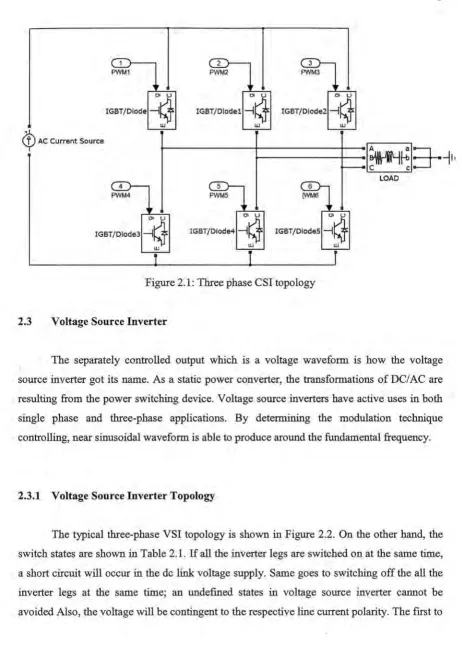
2.2 Current Source Inverter
The ac output current waveform is produce by using static power converter which
getting supply from de current supply. The frequency, phase, and magnitude should be
governable for the sinusoidal output. The generated load voltage which is nearly sinusoidal
OI U
IGBT/Dlode
-1~
w
PWM2
OI U
IGBT/Dlode1
-j~
w
OI U
IGBT/Diode2
-j~
w
5
¢
AC Current Source----l~~l3--1i·
OI U
IGBT/Dlode3
__,~
w
" ' u IGBT/Diode4
__,~
w
"' u
IGBT/DiodeS
-l~
[image:20.597.37.500.89.737.2]w
Figure 2.1: Three phase CS! topology
2.3 Voltage Source Inverter
LOAD
The separately controlled output which is a voltage waveform is how the voltage
source inverter got its name. As a static power converter, the transformations of DC/ AC are
resulting from the power switching device. Voltage source inverters have active uses in both
single phase and three-phase applications. By determining the modulation technique
controlling, near sinusoidal waveform is able to produce around the fundamental frequency.
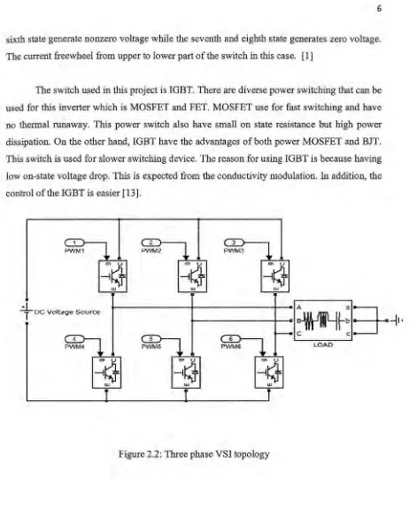
2.3.1 Voltage Source Inverter Topology
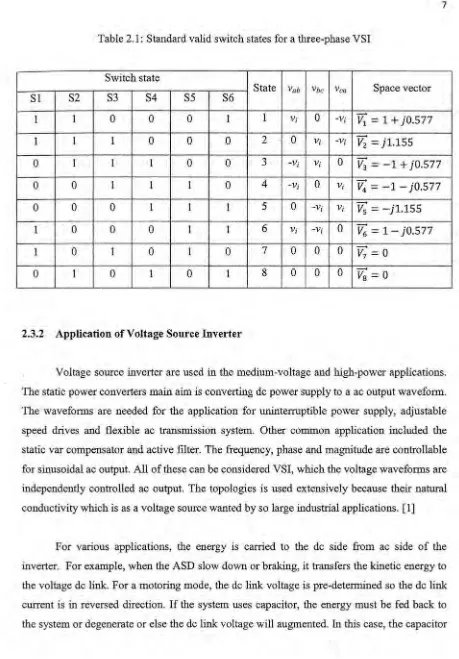
The typical three-phase VS! topology is shown in Figure 2.2. On the other hand, the
switch states are shown in Table 2.1. If all the inverter legs are switched on at the same time,
a short circuit will occur in the de link voltage supply. Same goes to switching off the all the
inverter legs at the same time; an undefined states in voltage source inverter cannot be
6
sixth state generate nonzero voltage while the seventh and eighth state generates zero voltage.
The current freewheel from upper to lower part of the switch in this case. [ 1]
The switch used in this project is IGBT. There are diverse power switching that can be
used for this inverter which is MOSFET and FET. MOSFET use for fast switching and have
no thermal runaway. This power switch also have small on state resistance but high power
dissipation. On the other hand, IGBT have the advantages of both power MOSFET and BJT.
This switch is used for slower switching device. The reason for using IGBT is because having
low on-state voltage drop. This is expected from the conductivity- modulation. In addition, the
control of the IGBT is easier [13].
2 3
PWM2 PWM3
~~
O> u "' u-;~
-;~
w w w
4-
o
c
Voltage Source1~~:1=t-~I
·
LOAD
"' u "' u "' u
-;~
-;~
-;~
[image:21.597.48.510.76.661.2]w UJ w
7
Table 2.1: Standard valid switch states for a three-phase VSI Switch state
State Vab Vbc Vea Space vector
Sl S2 S3 S4 S5 S6
1 1 0 0 0 1 1 V; 0 -V;
v;
=
1+
j0.5771 1 1 0 0 0 2 0 V; -V; --+ V
2
=
jl.1550 1 1 1 0 0 3 -V; V; 0 --+ V
3
=
-1+
j0.5770 0 1 1 1 0 4 -V; 0 V;
-
V4
=
-1 - j0.5770 0 0 1 1 1 5 0 -V; V;
v;
=
- jl.1551 0 0 0 1 1 6 V; -V; 0
v;
=
1 - j0.5771 0 1 0 1 0 7 0 0 0 --+ V
7
=
O0 1 0 1 0 1 8 0 0 0 --+ V
8
=
02.3.2 Application of Voltage Source Inverter
Voltage source inverter are used in the medium-voltage and high-power applications.
The static power converters main aim is converting de power supply to a ac output waveform.
The waveforms are needed for the application for uninterruptible power supply, adjustable
speed drives and flexible ac transmission system. Other common application included the
static var compensator and active filter. The frequency, phase and magnitude are controllable
for sinusoidal ac output. All of these can be considered VSI, which the voltage waveforms are
independently controlled ac output. The topologies is used extensively because their natural
conductivity which is as a voltage source wanted by so large industrial applications. [ 1]
For various applications, the energy is carried to the de side from ac side of the
inverter. For example, when the ASD slow down or braking, it transfers the kinetic energy to
the voltage de link. For a motoring mode, the de link voltage is pre-determined so the de link
[image:22.597.33.492.81.740.2]8
is connected with the resistor in parallel. Other alternative is feeding the energy to the system
but the method need a reversible current topology. There are other kinds of approach to use
the active rectifier for regeneration mode where it is the natural mode of the system.
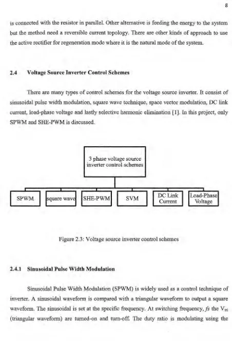
2.4 Voltage Source Inverter Control Schemes
There are many types of control schemes for the voltage source inverter. It consist of
sinusoidal pulse width modulation, square wave technique, space vector modulation, DC link
current, load-phase voltage and lastly selective harmonic elimination [l]. In this project, only
SPWM and SHE-PWM is discussed.
3 phase voltage source inverter control schemes
I
.
.
.
.
.
[image:23.597.35.487.76.748.2]SPWM square wave SHE-PWM SVM DC Current Link Load-Phase Voltage
Figure 2.3: Voltage source inverter control schemes
2.4.1 Sinusoidal Pulse Width Modulation
Sinusoidal Pulse Width Modulation (SPWM) is widely used as a control technique of
inverter. A sinusoidal waveform is compared with a triangular waveform to output a square
waveform. The sinusoidal is set at the specific frequency. At switching frequency,
fs
the V tri9
frequency of the control signal. The switching frequency will contain harmonics because the switching frequency affects the output of inverter. The duty cycle of one of the inverter
switches is amplitude modulation, ma. [2]
The Ycontrozcompared with Y1ri are given as follows.
V A - -_ Vdc
2
V A - - -_ Vdc
2
(2.1)
(2.2)
The frequency modulation ratio, m1 and amplitude modulation ratio, ma is deliberate
using the formula below.
peak amplitude of Vcontrol m =
-a amplitude of Vtri (2.3)
PWM frequency,f5
m -
-! - fundamental frequency,f1
(2.4)
The mf (frequency modulation) has to be an odd integer. The sub harmonics can exist
if 1the mf is not an integer. On the other hand, a de component may exist in the output voltage
if the frequency modulation is even number [3].
0.5
[image:24.600.34.503.66.674.2]·0.5