Abstract—This paper proposes a novel DC-DC converter topology to achieve an ultra-high step-up ratio while maintaining a high conversion efficiency. It adopts a three degree of freedom (3DoF) approach in the circuit design. It also demonstrates the flexibility of the proposed converter to combine with the features of modularity, electrical isolation, soft-switching, low voltage stress on switching devices, and is thus considered to be an improved topology over traditional DC-DC converters. New control strategies including the two-section output voltage control and cell idle control are also developed to improve the converter performance. With the cell idle control, the secondary winding inductance of the idle module is bypassed to decrease its power loss. A 400-W DC-DC converter is prototyped and tested to verify the proposed techniques, in addition to a simulation study. The step-up conversion ratio can reach 1:14 with a peak efficiency of 94% and the proposed techniques can be applied to a wide range of high voltage and high power distributed generation and DC power transmission.
Index Terms—Boost converter, control strategy, DC-DC power conversion, degrees of freedom (DoF), high step-up converter, modularization.
I.INTRODUCTION
Distributed Generation (DG) is playing an increasingly important role in reducing greenhouse gas emissions and improving the quality of human lives. In these systems, power converters are a key component to control power flow within the system. In particular, high step-up DC-DC converters are widely used in solar power generation, fuel cells, electric vehicles and uninterrupted power supplies (UPS) [1]-[13]. The features of DC-DC conversion are also essential to off-shore wind power transmission through HVDC power systems
Manuscript received November 26, 2014; revised May 4, 2015 and August 9, 2015; accepted September 29, 2015. This work is sponsored by the EPSRC of UK (EP/L00089X/1) and NSFC of China (51361130150).
Copyright © 2010 IEEE. Personal use of this material is permitted. However, permission to use this material for any other purposes must be obtained from the IEEE by sending a request to [email protected].
Y. Hu, P. Li and S. Finney are with the College of Electrical Engineering, Zhejiang University, Hangzhou, 310027, China; and the Department of Electronic and Electrical Engineering, University of Strathclyde, Glasgow, U.K.
J. Wu is with the College of Electrical Engineering, Zhejiang University, Hangzhou 310027, China (e-mail: [email protected]).
W. Cao is with the School of Electronics, Electrical Engineering and Computer Science, Queen’s University Belfast, Belfast, U.K.
Y. Li is with the Department of Electronic and Electrical Engineering, University of Strathclyde, Glasgow, UK.
[14][15]. In these applications, high voltage gain and high conversion efficiency of DC-DC converters are highly desirable.
When isolated topologies are utilized, a high voltage gain is traditionally achieved by manipulating the transformer’s turns ratio, the PWM duty ratio or phase-angle shift. The duty ratio of high-frequency switching devices is often considered as one design freedom while the turns ratio of transformers is another [16]-[28]. When both are employed to achieve a high voltage conversion ratio, it is termed the two degrees of freedom (2DoF) design [17][21][23]. Furthermore, soft-switching can also be a useful feature when an active or passive clamping circuit is implemented [4]-[6]. An active clamping circuit consists of one active switching device and one clamping capacitor, while a passive clamping circuit uses some passive switching devices (e.g. diodes) for the same purpose. In theory, the leakage inductance is proportional to the square of the turns ratio [29]. As a result, a very high turns ratio is generally avoided in the transformer design since it can reduce the efficiency of the transformer. A typical topology of high step-up converters uses only one switching device [30][31] while their converter ratings are low. Due to the size of capacitors, the power density of these converters decreases as the voltage gain increases [32]-[34]. In the literature, some high step-up conversion ratios are also reported by combining the features of turns ratio, multi-level and duty ratio in the converter design [35]-[41]. For instance, paper [41] integrates a coupled inductor with a switching capacitor in the high step-up converter using one switching device. The input-parallel output-series structure can also provide a high voltage gain and a high power level [42][43]. In paper [42], coupled inductors are used to achieve a high voltage gain but electrical isolation is absent. Alternatively, the use of a cascaded converter structure can provide a high voltage gain [44][45]. However, the topology in [44] is limited in converter power ratings due to the high current in the switching devices. In order to increase the power level, a modular multilevel converter is presented in [45] but it can only regulate the duty ratio and cell number (i.e. 2DoF). Clearly, these reported topologies do not provide electrical isolation and sufficient flexibility for further expansion.
The voltage gain of a typical 2DoF converter is expressed as:
2
1
N
G
D
(1)where N is the turns ratio and D is the duty ratio.
Obviously, a small change in the duty ratio can lead to a significant change in the voltage gain. This poses a challenge to
Yihua Hu,
Senior Member IEEE
, Jiande Wu, Wenping Cao,
Senior Member,
Weidong Xiao,
Senior Member, IEEE
, Peng Li, Stephen Finney, Yuan Li
Ultra-High Step-up DC-DC Converter for
Distributed Generation by Three Degrees of
Freedom (3DoF) Approach
the converter control so that the accurate regulation of the output voltage becomes difficult. To tackle the problem, this paper proposes a novel ultra-high step-up DC-DC converter, which utilizes the features of modularity, multi-levels and electrical isolation. In effect, this is a three degree of freedom (3DoF) design of DC-DC converters.
II. PROPOSED 3DOFCONVERTER TOPOLOGY
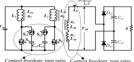
A conventional interleaved flyback-forward DC-DC converter is presented in Fig. 1(a). The voltage gain can be found by:
2
2
1
1
2
1
(1
)
outin LK s
V
N
G
V
D
L
f
D R
(2)
where LLK is the leakage inductance, fs is the switching frequency, and R is the load resistance. Clearly, the voltage gain is determined by the leakage inductance of the coupled inductor, switching frequency, load resistance, in additional to turns ratio and duty ratio.
Do1
Do2 Co1
Co2 R
S1 S2 Vin
Cc2
Cc1
n1 n1
n2
n2
Lk
Sc1 Sc2
L1a L2a
L2b
L1b
* *
L1 L2
Vab
Control freedom: turn ratio Control freedom: turn ratio
(a) Typical Flyback-forward converter [6]
* Do1
Do2 Co1
Co2 R
*
Vab LLk1
LLk2 n2
L1b n2 L2b
n2 L3b
n2 L4b
LLk4 LLk3 S1 S2
Cc2 Cc1
n1 n1
Sc2
L1a L2a
S3 n1
Sc3 L3a
Sc1
Cc3 L1 L2 L3
S4 n1
Sc4 L4a
Cc4 L4 Vin
Vcell-1
Vcell-2
[image:2.612.327.557.237.535.2](b)Proposed flyback-forward DC-DC converter (using two cells)
Fig. 1 DC-DC converter topologies with flyback-forward cells.
If the secondary side of the flyback-forward DC-DC converter is seen as a cell, more cells can be added up in series, as shown in Fig. 1(b). By doing so, a multi-level output voltage can be obtained. The corresponding voltage gain in an idea condition is given by:
2
1
m N
G
D
(3) where m denotes the number of voltage levels.This paper develops a two-cell high step-up DC-DC converter as an example and its topology is shown in Fig. 1(b), where S1-S4 are four main switches. Active clamping circuits including clamp switches Sc1-Sc4 and clamping capacitors
Cc1-Cc4 are employed to limit the voltage stress on the main switches. Four coupled inductors L1-L4, are used to form two
power cells (L1 and L2 for cell-1, L3 and L4 for cell-2). The primary and secondary winding turns for the four coupled inductors are represented by n1 and n2,respectively, and their turns ratio is N = n2/n1. The coupling references are remarked with ―*‖, ―○‖, ―□‖ and ― ▍‖. LLK1-LLK4 are the leakage inductances for coupled inductors L1-L4, respectively. In this figure, the rectifier diodes Do1-Do2 and the output capacitors
C1-C2 also form a voltage-doubling rectifier circuit.
The proposed converter is built on basic cells; each of them consists of two coupled inductors and a power switch. Typical steady-state waveforms of this converter are shown in Fig. 2. The active clamping switches SC1-SC 4 are complementary to the main switches S1-S4, respectively. The outputs of cell-1 and cell-2 are Vcell-1 and Vcell-2, respectively. The switches S1-S4 can be regulated by earthier duty ratio control or phase angle shift control. The waveforms of Vcell-1 and Vcell-2 are identical.
Vgs3
iL1a
iS1
iS2
vds1
vds2
vDo2
iDo2
iL2a iL1a
iS1 iS2
vds2
vDo2
t0 t1 t2t3t4 t5
Vgs3
Vgs4 Vgsc4
Vgsc3
iL2a
vds1
vdsc2
vdsc2
t6t7 t8 t9t10t11t12 t13t14 t15t16
iCc2
iCc2
Vgsc4
Vgs4
Vgsc3
Vgs3
Vgs4
Vgs1
Vgs1
Vgs2 Vgsc2
Vgsc1
Vgsc2
Vgs2
Vgsc1
Vgs1
Vgs2
Vcell-1
Vab
Vcell-1 V ab
iDo2
Fig. 2 Waveforms of the proposed converter.
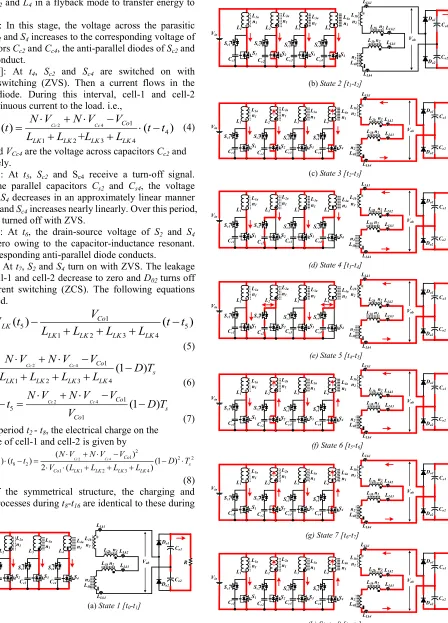
The proposed converter has eight operational stages, as shown in Fig. 3.
State 1 [t0-t1]: During this stage, S1~S4 are turned on and the corresponding clamping switches are off. All the coupled inductors operate in flyback mode to store energy. The outputs of cell-1 and cell-2 are zero and the output rectifier diodes are both reverse-biased. The output capacitors C01and C02 supply the energy to the load.
State 2 [t1-t2]: At t1, S2 and S4 receive a turn-off gate signal, increasing their drain-source voltage across the parasitic capacitor of the main switches in an approximate linear manner. Due to the low parasitic capacitance and the large current in the primary coupled inductor, this period is very short.
[image:2.612.56.289.300.409.2]mode while L2 and L4 in a flyback mode to transfer energy to the load.
State 4 [t3-t4]: In this stage, the voltage across the parasitic capacitor of S2 and S4 increases to the corresponding voltage of clamp capacitors Cc2 and Cc4, the anti-parallel diodes of Sc2 and
Sc4 begin to conduct.
State 5 [t4-t5]: At t4, Sc2 and Sc4 are switched on with zero-voltage switching (ZVS). Then a current flows in the anti-parallel diode. During this interval, cell-1 and cell-2 provide a continuous current to the load. i.e.,
2 4 1
1 4
1 2 3 4
( )
(
)
+
Cc Cc Co
LK
LK LK LK LK
N V
N V
V
i
t
t t
L
L
L
L
(4)where VCc2 and VCc4 are the voltage across capacitors Cc2 and
Cc4, respectively.
State 6 [t5-t6]: At t5, Sc2 and Sc4 receive a turn-off signal.
Because of the parallel capacitors Cs2 and Cs4, the voltage across S2 and S4 decreases in an approximately linear manner and that in Sc2 and Sc4 increases nearly linearly. Over this period,
Sc2 and Sc4 are turned off with ZVS.
State 7 [t6-t7]: At t6, the drain-source voltage of S2 and S4 decrease to zero owing to the capacitor-inductance resonant. Then, the corresponding anti-parallel diode conducts.
State 8 [t7-t8]: At t7, S2 and S4 turn on with ZVS. The leakage currents of cell-1 and cell-2 decrease to zero and D02 turns off with zero-current switching (ZCS). The following equations can be obtained.
1
1 5 5
1 2 3 4
( )
( )
Co(
)
LK LK
LK LK LK LK
V
i
t
I
t
t t
L
L
L
L
(5)
2 4 1
5
1 2 3 4
( )
Cc Cc Co(1
)
LK s
LK LK LK LK
N V
N V
V
I
t
D T
L
L
L
L
(6)2 4 1
8 5
1
(1
)
Cc Cc Co
s Co
N V
N V
V
t
t
D T
V
(7) During the period t2 - t8, the electrical charge on the
secondary side of cell-1 and cell-2 is given by
2 4
2
1 2 2
1 1 5 8 2
1 1 2 3 4
( )
1
( ) ( ) (1 )
2 2 ( )
Cc Cc Co
Co LK s
Co LK LK LK LK
N V N V V
Q I t t t D T
V L L L L
(8) Because of the symmetrical structure, the charging and discharging processes during t8-t16 are identical to these during
t0-t7.
* LLk1 LLk2 n2 L1b n2 L2b n2 L3b n2 L4b LLk4 LLk3 Do1 Do2 Co1 Co2 R S1 S2
Cc2 Cc1
* n1 n1
Sc2 L1a L2a
S3 n1 Sc3 L3a Sc1 Cc3 L1 L2 L3 Vin S4 n1 Sc4 L4a Cc4 L4 Vab
(a) State 1 [t0-t1]
* LLk1 LLk2 n2 L1b n2 L2b n2 L3b n2 L4b LLk4 LLk3 Do1 Do2 Co1 Co2 R
S1 S2
Cc2 Cc1
* n1 n1
Sc2
L1a L2a
S3 n1 Sc3 L3a Sc1 Cc3
L1 L2 L3
Vin S4 n1 Sc4 L4a Cc4 L4 Vab
(b) State 2 [t1-t2]
S1 S2 Cc2 Cc1
* n1 n1
Sc2 L1a L2a
S3 n1 Sc3 L3a Sc1 Cc3 L1 L2 L3 Vin S4 n1 Sc4 L4a Cc4 L4 * LLk1 LLk2 n2 L1b n2 L2b n2 L3b n2 L4b LLk4 LLk3 Do1 Do2 Co1 Co2 R Vab
(c) State 3 [t2-t3]
* LLk1 LLk2 n2 L1b n2 L2b n2 L3b n2 L4b LLk4 LLk3 Do1 Do2 Co1 Co2 R S1 S2
Cc2 Cc1
* n1 n1
Sc2 L1a L2a
S3 n1 Sc3 L3a Sc1 Cc3 L1 L2 L3 Vin S4 n1 Sc4 L4a Cc4 L4 Vab
(d) State 4 [t3-t4]
* LLk1 LLk2 n2 L1b n2 L2b n2 L3b n2 L4b LLk4 LLk3 Do1 Do2 Co1 Co2 R S1 S2
Cc2 Cc1
* n1 n1
Sc2 L1a L2a
S3 n1 Sc3 L3a Sc1 Cc3 L1 L2 L3 Vin S4 n1 Sc4 L4a Cc4 L4 Vab
(e) State 5 [t4-t5]
S1 S2 Cc2 Cc1
* n1 n1
Sc2 L1a L2a
S3 n1 Sc3 L3a Sc1 Cc3 L1 L2 L3 Vin S4 n1 Sc4 L4a Cc4 L4 * LLk2 n2 L1b n2 L2b n2 L3b n2 L4b LLk4 LLk3 Do1 Do2 Co1 Co2 R Vab LLk1
(f) State 6 [t5-t6]
S1 S2 Cc2 Cc1
* n1 n1
Sc2 L1a L2a
S3 n1 Sc3 L3a Sc1 Cc3 L1 L2 L3 Vin S4 n1 Sc4 L4a Cc4 L4 * LLk2 n2 L1b n2 L2b n2 L3b n2 L4b LLk4 LLk3 Do1 Do2 Co1 Co2 R Vab LLk1
(g) State 7 [t6-t7]
S1 S2 Cc2 Cc1
* n1 n1
Sc2 L1a L2a
S3 n1 Sc3 L3a Sc1 Cc3 L1 L2 L3 Vin S4 n1 Sc4 L4a Cc4 L4 * LLk2 n2 L1b n2 L2b n2 L3b n2 L4b LLk4 LLk3 Do1 Do2 Co1 Co2 R Vab LLk1
[image:3.612.104.552.54.677.2](h) State 8 [t7-t8]
III. STEADY STATE ANALYSIS
In order to simplify the analysis of the proposed converter, the following assumptions are made: i) all the four coupled inductors are identical; ii) all the clamping capacitors are identical; iii) the voltage of the clamping capacitors is constant; iv) the dead-time between the main switches and clamping switches is neglected.
A. Voltage stress
The voltage stress on switching devices is equal to the voltage across the clamping capacitors.
1
inDSi Cci
V
V
V
D
(9) where VCci is the voltage of the active clamping switch, VDSi is the voltage of the main switch, and Vin is the input voltage. According to the symmetrical waveforms of Vab, the voltage stress on the output diodes can be found by:
V
co1
V
co2
V
out (10)B. Voltage gain
However, the leakage inductance of the coupled inductor can also impact on the voltage gain. In a two-level high step-up converter, the electrical charge of Co1 is half of the total electrical charge due to the symmetry of the rectifier circuit.
1
1
2
out
Co s
V
Q
T
R
(11) From (8), (9) and (11), the voltage gain can be expressed as
1 2 3 4
4
2
(
)
1
s LK LK LK LKN
G
f
L
L
L
L
D
R
(12) where R is the load resistance.
Due to the series connection of the secondary side of the high step-up power cells, the turns ratios of the coupled inductors in power cells can be different. Under normal conditions, the total voltage gain of M cells is:
1
1
2 (
)
2
(
)
1
m
i i
m
s LKi
i
N
G
f
L
D
R
(13) where Ni is the turns ratio of the ith cell; and LLki is the leakage
inductance of the ith cell.
C. Soft-switching
Soft-switching of power devices can reduce the switching power loss and thus improve the energy efficiency of the converter. In order to realize ZVS for the clamp switches, the antiparallel diodes of clamp switches should conduct prior to the turn-on of the switches. For the main switches, the energy stored in parasitic capacitors should be lower than that stored in the leakage inductor. The ZVS turn-on condition for the main switches is
2 2
2
1
1
2
2
LKi
i DSi DSi
i
L
I
C V
N
(14) where Ii is the primary input current of the power step-up cell and CDSi is the parasitic capacitor voltage.Owing to the series connection of the secondary side of high step-up power cells, the leakage inductance can be easily increased for soft-switching at the expense of the voltage gain, as presented in (12).
IV.CONTROL STRATEGIES FOR THE PROPOSED CONVERTER
There are two control strategies developed to control the output voltage of the proposed converter: the two-section output voltage control and the module idle control.
A. Two-section output voltage control
In the proposed converter, the output voltage is built up by connecting several voltage sources in series, similar to Fig. 1(b). Therefore, the total voltage gain is the sum of individual cells. The output voltage of m cells includes two parts: the output voltage of m-1 cells, and power cell m (used for minor adjustment of the output voltage to limit the duty ratio change).
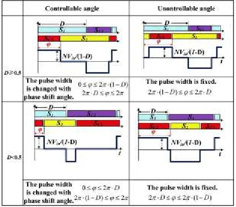
Moreover, the phase-angle shift with respect to the turn-on signal of S1 (see Fig. 2) can be employed to adjust the output
[image:4.612.113.247.508.583.2]voltage of each cell. This has two conditions: controllable and uncontrollable, as illustrated in Fig. 4. The output voltage control under D≥0.5 and D<0.5 is further presented in Fig. 5. At a shift angle of 180°, the output voltage peaks. In the power cell, the two main switches are usually of 180° shift angle, which is in an uncontrollable range, as shown in Figs. 4 and 5. When all cells use the same duty ratio, the phase-angle shift can be employed to control the converter output voltage.
[image:4.612.322.557.520.726.2]Fig. 6 illustrates the proposed converter control strategy. Δ Vref is the threshold value of voltage error. For a given voltage error, major and minor adjustments can be decided. If a major adjustment is needed, all the high step-up power cells are involved and a new duty ratio is assigned. In a minor adjustment, only the mth power cell is involved. If the voltage error is positive, the duty ratio of associated main switches needs to be increased. When the voltage error is negative, the phase-angle shift is employed to control the output voltage.
(a) 0.66 duty ratio
[image:5.612.57.287.46.443.2]
(b) 0.33 duty ratio
Fig. 5 Output voltage with the phase-angle shift control.
Vref
Vout
+
-PI
ref
V V
ref
V V
PI
Duty ratio Power cell (1~M)
0
V
0
V
Duty ratio
Power cellthe Mth
PI Phase shift angle
Power cell the Mth Fig. 6 Schematic diagram of the proposed control strategy.
B. Cell idle control
In the proposed topology, power cell idle conditions can be employed to adjust the voltage gain. If the primary main switching devices are idle, the secondary winding inductor changes from an alternating square voltage source to an inductor. Since the secondary windings of the coupled inductor are series connected; the winding inductance of the idle power cell blocks the current, which is generated from other cells. In this paper, a shielding control strategy is developed for idle power cells by controlling the coupled inductor output with reverse polarity. It is needed to send a turn-off signal to the main switching devices and a turn-on signal to the idle power cells, as presented in Fig. 7. The output of Vcell-2is zero during [t1-t2] and [t3-t4] that ensures the energy flow from Vcell-1 to the load. The equivalent circuit of the idle power cell is shown in Fig. 8. Both L3 and L4 operate in flyback mode, and the secondary side voltage sources are effectively reverse connected. At this condition, the secondary inductor of the idle module is bypassed. In the idle cells, the power losses (associated with the wire resistance and on-state conducting loss of clamp switches) are very low. In effect, cell-1 can operate at the rated output power so as to improve the converter efficiency.
iL3a
Vcell-2
iL3a iL4a
t0 t2 t3
Vgsc4
Vgsc3
iL4a
Vab
t4 t5
Vgsc4
Vgs4
Vgsc3
Vgs3
Vgs1
Vgs1
Vgsc2
Vgsc1
Vgsc2
Vgs2
Vgsc1
Vgs1
Vgs2 Vgsc2
Vcell-1
Vcell-1
Vcell-2
[image:5.612.317.559.52.363.2]t1
Fig. 7 Waveforms of the shielding control under modular power cell idle conditions.
n1
L3a
L3 n1
Cc4
L4
n2
L3b
n2
L4b
LLk4
LLk3
Vcell-2
Cc3
G3Vin
G4Vin
L4a
LLk3
LLk4
Fig. 8 Equivalent circuit of the idle modular power cell.
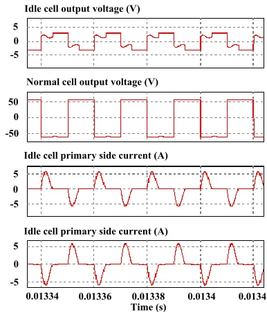
In order to study the mechanism of the cell idle mode, the PSIM simulation software is employed to model the converter. In Fig. 9, a two-cell topology is used as an example. The input voltage is 15 V and the turn ratio is 2. One cell is idle and the other cell is operational. The output voltage of the operating cell is 60 V while the peak output voltage of the idle cell is 3 V, which is associated with the leakage inductance.
0.01334
Time (s) -5
0 5 -5 0 5 -50 0 50 -5 0 5
Idle cell output voltage (V)
Normal cell output voltage (V)
Idle cell primary side current (A)
Idle cell primary side current (A)
[image:5.612.338.531.481.707.2]0.01336 0.01338 0.0134 0.01342
V. EXPANDABLE CHARACTERISTIC AND
PERFORMANCE COMPARISON
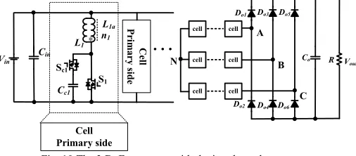
The proposed 3DoF topology is flexible and expandable. First, it can combine with the interleaved structure to expand the power level, as shown in Fig. 10. Furthermore, with the development of high voltage silicon carbine (SiC) devices [46], the topology can be applied to high voltage DC (HVDC) power transmission for offshore wind power. In the simulation, the input voltage is 100 V, converter power is 100 kW, switching frequency is 50 kHz, each winding arm has 4 cells. Simulation results are shown in Fig. 11. The output voltage reaches 6.35 kV (the voltage gain is 63.5). The voltage stress on the primary switching devices is only 200 V and the peak current is 125 A. Furthermore, more diode bridges and winding arms can be added up for a higher output power.
S1 Cc1
* n1
L1a
Sc1 L1
Cin
Vout R
Do2 Do3
Do4 Do5
Do6 Co
Vin
C
ell
P
rim
ar
y s
id
e
Cell Primary side
cell cell
cell cell
cell cell
Do1
N
A
B
[image:6.612.334.536.54.491.2]C
Fig. 10 The 3 DoF converter with the interleaved structure.
Currently, the input-parallel output-series structure is widely used to achieve a high voltage output. However, it needs a large number of diodes and capacitors to connect the secondary sides of all cells in series after the rectifier circuit, increasing connection complexity and fault possibilities. Furthermore, the structure cannot be used to achieve a high power output. In this paper, a new solution is to combine with the input-parallel output-series structure, as shown in Fig. 12. In this case, the 3DoF topology can be seen as a cell in the traditional input-parallel output-series topology to build up a high-voltage-gain converter. Clearly, the features of interleaved structure and input-parallel output-series structure can be used in the proposed 3DoF to increase both power and voltage, as shown in Fig. 13. Therefore, by introducing a new design freedom, the proposed topology can incorporate features of traditional input-parallel output-series converters to increase voltage (via series-connection) and power (via parallel-connection) to meet the requirements.
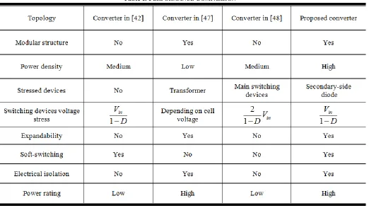
Based on the above analysis, a performance comparison of different DC-DC converter topologies is presented in Table I. Compared with the topologies in [42][47], the proposed topology has a higher power density. Compared with the converter in [48], the proposed topology can provide electrical isolation and soft-switching. Furthermore, the secondary diodes can be achieved by connecting low-voltage diodes in series and parallel connections [49]-[50].
-2k 0k 2k -2k 0k 2k -2k 0k 2k
0.01448 0.0145 0.01454 Time (s)
6.32k 6.33k 6.34k
Vout(V)
VNA(V)
VNB(V)
VNC(V)
0.01452
(a) Output voltage and winding arm output.
-50 0 50 0 62.5 125 0 100 200 0 100 200
VDS(V)
VDSc(V)
IDS(A)
IDSc(A)
0.01448 0.0145 0.01454 Time (s)0.01452
(b) Voltage and current of the primary switching devices Fig. 11 Simulation results for the 3DoF with the interleaved
[image:6.612.49.302.232.343.2]Energy conversion
topology
Energy conversion
topology
Energy conversion
topology
Rectifier Circuit
Load Rectifier
Circuit
Rectifier Circuit
Energy conversion
topology
Energy conversion
topology
Energy conversion
topology
Rectifier Circuit
Input Output
[image:7.612.48.238.49.336.2]Proposed 3 DoF topology
Fig. 12 The 3 DoF converter with the input-parallel output-series structure.
S1 Cc1
* n1
L1a
Sc1
L1 C
ell
P
rim
ar
y s
id
e
Cell Primary side
cell cell
cell cell
cell cell
N
A
B
C
Energy conversion
topology
Energy conversion
topology
Energy conversion
topology
Rectifier Circuit
Load Rectifier
Circuit
Rectifier Circuit
[image:7.612.333.555.51.305.2]Input Output
Fig. 13 Proposed 3 DoF converter for high power and high voltage-gain output.
[image:7.612.57.579.393.687.2]VI. EXPERIMENTAL VERIFICATION
A converter with two cells is designed and fabricated to verify the effectiveness of the proposed converter. The system parameters are tabulated in Table II. The coupled inductor is constructed from a Koolmu magnetic core (0077109A7). Table III lists the parameters of four coupled inductors.
TABLE II.SPECIFICATIONS OF THE PROPOSED CONVERTER
Component/Parameter Value
Power level (Pout) 400 W
Input voltage (Vin) 5~10 V
Load resistance (R) 44 Ω
Output voltage (Vout) 50~100 V
Switching frequency (fs) 50 kHz
Main switches (S1~ S4) FDP047AN
Clamp switches (Sc1~ S c4) FDP047AN
Rectifier diodes (Do1, Do2) FEP30DP
Clamp capacitors (Cc1 ~ Cc4) 4.7 μF
Output capacitor (Co1 and Co2) 470 μF
Turns ratio (N=n2/n1) 40:10
TABLE III.SPECIFICATIONS OF THE COUPLED INDUCTORS
Primary inductance
Primary leakage inductance
Secondary inductance
Secondary leakage inductance
L1 28.65 μH 1.041 μH 442.9 μH 7.651 μH
L2 29.27 μH 0.991 μH 453.5 μH 7.684 μH
L3 28.88 μH 1.002 μH 447.3 μH 7.684 μH
L4 28.81 μH 0.980 μH 446.5 μH 7.886 μH
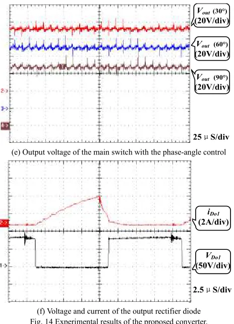
Experimental results are presented in Fig. 14 for a 5 V input voltage, 0.5 duty ratio, and 180° shift angle. Fig. 14(a) presents the cell output voltage under normal conditions using the same duty ratio and phase angle shift for cell-1 and cell-2 where each cell generates half of the output voltage. Fig. 14(b) and (c) show test results for cell-2 idle, without and with the shielding control, respectively. In Fig. 14(b), the input current is limited so that the converter cannot transfer energy to the load. The power generated from the operating module cell is largely absorbed by the idle power cell so that little power is transferred to the load. With the shielding control strategy (see Fig. 14(c)), the energy can be transferred to the secondary side without incurring a voltage drop across the idle windings and the input current increases dramatically. Fig. 14(d) presents the gate signal with the two-section output voltage control where the phase-angle shift control is employed to realize minor voltage adjustment. In cell-1 of Fig. 14(d), S1 and S2 are with a 50% duty ratio and an 180o phase angle shift. In cell-2, S3 and S4 are with also with
a 50% duty ratio but a 150o phase angle shift. Compared with S1,
there is a 30o delay for S3. S2 and S4 have the same phase shift angle and their output voltage is 72 V. Fig. 14(e) shows the output voltage of main switch S3 with a shift angle of 30°, 60° and 90°; the corresponding output voltage are 72V, 70V and 67V, respectively. The output voltage is fairly smooth with the phase-angle control. Fig. 14(f) presents the voltage and current waveforms for the output rectifier diode. Clearly, the rectifier diode reverse-recovery problem is alleviated.
10μS/div Vab
(50V/div)
Vcell-1
(25V/div)
(a) Cell output voltage under normal conditions
10μS/div
Vcell-2
(25V/div)
Vab
(5V/div)
iin
(1A/div)
(b) Without the shielding control
10μS/div
Vab
(25V/div)
iL3
(10A/div)
iin
(10A/div)
(c) With the shielding control
VGS1
(10V/div)
VGS2
(10V/div)
VGS3
(10V/div)
VGS4
(10V/div)
5μS/div
Vout (30°)
(20V/div)
Vout (60°)
(20V/div)
Vout (90°)
(20V/div)
25μS/div
(e) Output voltage of the main switch with the phase-angle control
2.5μS/div
VDo1
(50V/div)
iDo1
(2A/div)
[image:9.612.55.287.49.370.2](f) Voltage and current of the output rectifier diode Fig. 14 Experimental results of the proposed converter.
The soft-switching performance of the main switch (S1) and clamping switch (SC1) is demonstrated in Fig. 15. Due to the symmetry of the topology, all the switches have the same current and voltage profiles. Experimental results from the load transient tests are shown in Fig. 16. Fig. 16(a) shows the response to a step load change from 44 to 24 Ω and Fig. 16(b), step load increase from 24 to 44 Ω. With the closed-loop control, the output voltage can quickly return to the set voltage, showing excellent robustness of the system. The single cell efficiency, one-cell-operating one-cell-idle efficiency and overall converter efficiency are calculated and presented in Fig. 17. In the power cell idle condition, due to the parasitic resistance in the primary-side capacitors and inductors and secondary winding resistance of the idle cell, the converter efficiency is lower than that for a single cell working condition; but is higher than the two-cell operating condition. By using power cells in an idle mode, the converter can maintain a relatively high efficiency over a wide output power range.
10 μS/div
Vgs
10V/div
Vds
20V/div
ids
25A/div
(a) Soft-switching of the main switch
10 μS/div
Vgssc
10V/div
Vdssc
20V/div
isc
25A/div
[image:9.612.321.550.51.202.2](b) Soft-switching of the active clamp switch Fig. 15 Soft-switching performance for S1 and SC1.
100ms/div
iin
40A/div
Vout
25V/div
(a) Step load change from 44 to 24 Ω
100ms/div
iin
30A/div
Vout
25V/div
(b) Step load change from 24 to 44 Ω Fig. 16 Load transient tests.
[image:9.612.323.545.215.726.2] [image:9.612.58.281.596.732.2]VII. CONCLUSION
This paper has presented an ultra-high step-up DC-DC topology based on a 3DoF topology. Through theoretical analysis and experimental tests, the proposed converter is proven to be advantageous.
i) A 3DoF design is achieved to improve the converter performance. The electrical isolation and modular structure of high step-up power cells are combined to increase the output voltage.
ii) The voltage stress on primary switching devices of the coupled inductors is limited and soft-switching of primary-side switches is achieved. The proposed 3DoF converter can use low-voltage power devices to generate a high output voltage. In addition, the reverse-recovery issue with secondary rectifier diodes is also alleviated.
iii) The two-section output voltage control and module idle control are developed to improve the controllability of the output voltage and converter efficiency over a wide power range.
In summary, the proposed converter is featured with electrical isolation, modularity, multi-level structure, controllable turns ratio and duty ratio, and flexible control strategies to provide high system performance. The developed techniques can be applied widely to high-voltage and high-power DC systems.
REFERENCES
[1] K.I. Hwu, Y.T. Yau, ―High step-up converter based on coupling inductor and bootstrap capacitors with active clamping,‖ IEEE Trans. Power Electron., vol. 29, no. 6, pp. 2655-2660, Jun. 2014.
[2] Y. Gu, X. Xin, W. Li, X. He, ―Mode-adaptive decentralized control for renewable DC microgrid with enhanced reliability and flexibility,‖ IEEE Trans. Power Electron., vol. 29, no.9, pp. 5072-5080, Sep. 2014. [3] Y. Park, B. Jung, and S. Choi, ―Nonisolated ZVZCS resonant PWM
DC-DC converter for high step-up and high-power applications,‖ IEEE Trans. Power Electron., vol. 27, no. 8, pp. 3568-3575, Aug. 2012. [4] W. Li, W. Li, X. Xiang, Y. Hu, X. He, ―High step-up interleaved
converter with built-in transformer voltage multiplier cells for sustainable energy applications,‖ IEEE Trans. Power Electron., vol. 29, no. 6, pp. 2829-2836, Jun. 2014.
[5] F. Evran, M.T. Aydemir, ―Isolated high step-up DC-DC converter with low voltage stress,‖ IEEE Trans. Power Electron., vol. 29, no. 7, pp. 3591-3603, Jul. 2014.
[6] W. Li, L. Fan, Y. Zhao, X. He, D. Xu, and B. Wu, ―High-step-up and high efficiency fuel-cell power-generation system with active-clamp flyback–forward converter,‖ IEEE Trans. Ind. Electron., vol. 59, no. 1, pp. 599-610, Jan. 2012.
[7] W. Li, X. He, ―Review of non-isolated high step-up DC/DC converters in photovoltaic grid-connected applications,‖ IEEE Trans. Ind. Electron., vol. 58, no.4, pp. 1239-1250, 2011.
[8] S.M. Chen, T.J. Liang, L.S. Yang, and J.F. Chen, ―A safety enhanced, high step-up dc–dc converter for ac photovoltaic module application,‖
IEEE Trans. Power Electron., vol. 27, no. 4, pp. 1809-1817, Apr. 2012. [9] G. Spiazzi, P. Mattavelli, and A. Costabeber, ―High step-up ratio flyback converter with active clamp and voltage multiplier,‖ IEEE Trans. Power Electron., vol. 26, no. 11, pp. 3205-3214, Nov. 2011.
[10] K.J. Lee, B.G. Park, R.Y. Kim, and D.S. Hyun, ―Nonisolated ZVT two-inductor boost converter with a single resonant inductor for high step-up applications,‖ IEEE Trans. Power Electron., vol. 27, no. 4, pp. 1966-1973, Apr. 2012.
[11] L.S. Yang, T.J. Liang, H.C. Lee, J.F. Chen, ―Novel high step-up DC-DC converter with coupled-inductor and voltage-doubler circuits,‖ IEEE Trans. Ind. Electron., vol. 58, no. 9, pp. 4196-4206, Sep. 2011. [12] K.B. Park, G.W. Moon, and M.J. Youn, ―High step-up boost converter
integrated with a transformer-assisted auxiliary circuit employing quasi-resonant operation,‖ IEEE Trans. Power Electron., vol.27, no.4, pp: 1974-1984, April 2012.
[13] I. Laird, and D.D.C. Lu, ―High step-up DC/DC topology and MPPT algorithm for use with a thermoelectric generator,‖ IEEE Trans. Power Electron., vol. 28, no. 7, pp. 3147-3157, Jul. 2013.
[14] M. Hajian, J. Robinson, D. Jovcic, B. Wu, ―30 kW, 200 V/900 V, thyristor LCL DC/DC converter laboratory prototype design and testing,‖ IEEE Trans. Power Electron., vol. 29, no. 3, pp. 1094-1102, Mar. 2014.
[15] W. Chen, A.Q. Huang, C. Li, G. Wang, and W.S. Gu, ―Analysis and comparison of medium voltage high power DC/DC converters for offshore wind energy systems,‖ IEEE Trans. Ind. Electron., vol. 28, no. 4, pp. 1987-1997, Apr. 2013.
[16] R.J. Wai, C.Y. Lin and Y.R. Chang, ―High step-up bidirectional isolated converter with two input power sources,‖ IEEE Trans. Ind. Electron., vol. 56, no.7, pp. 2629-2643, Jul. 2009.
[17] T. J. Liang, J. H. Lee, S. M. Chen, J. F. Chen, and L. S. Yang, ―Novel isolated high-step-up DC-DC converter with voltage lift,‖ IEEE Trans. Ind. Electron., vol. 60, no.4, pp. 1483-1491, Apr. 2013.
[18] G. Spiazzi, P. Mattavelli, and A. Costabeber, ―High step-up ratio flyback converter with active clamp and voltage multiplier,‖ IEEE Tran. Power Electronics, vol. 26, no. 11, pp. 3205-3214, Nov. 2011.
[19] M. Delshad, and H. Farzanehfard, ―High step-up zero-voltage switching current-fed isolated pulse width modulation DC-DC converter,‖ IET Power Electronics, vol. 4, no. 3, pp. 316-322, 2011.
[20] W. Li, and X. He, ―A family of isolated interleaved boost and buck converters with winding-cross-coupled inductors,‖ IEEE Trans. Power Electronics, vol. 23, no. 6, pp. 3164-3173, Nov. 2008.
[21] W. Li, L. Fan, Y. Zhao, X. He, D. Xu, and B. Wu, ―High-step-up and high-efficiency fuel-cell power-generation system with active-clamp flyback-forward converter,‖ IEEE Trans. Ind. Electron., vol. 59, no. 1, pp. 599-610, Jan. 2012.
[22] B. Yuan, X. Yang, X. Zeng, J. Duan, J. Zhai, and D. Li, ―Analysis and design of a high step-up current-fed multiresonant DC-DC converter with low circulating energy and zero-current switching for all active switches,‖ IEEE Trans. Ind. Electron., vol. 59, no. 2, pp. 964-978, Feb. 2012.
[23] Y. Zhao, X. Xiang, W. Li, and X. He, ―Advanced symmetrical voltage quadrupler rectifiers for high step-up and high output-voltage converters,‖ IEEE Trans. Power Electronics, vol. 28, no. 4, pp. 1622-1631, Apr. 2013.
[24] C.T. Pan, C.M. Lai, and M.C. Cheng, ―A novel integrated single-phase inverter with auxiliary step-up circuit for low-voltage alternative energy source applications,‖ IEEE Trans. Power Electronics, vol. 25, no. 9, pp. 2234-2241, Sep. 2010.
[25] F. Forest, T.A. Meynard, X.E. Laboure, B. Gelis, J. J. Huselstein, and J.C. Brandelero, ―An isolated multicell intercell transformer converter for applications with a high step-up ratio,‖ IEEE Trans. Power Electronics,
vol. 28, no. 3, pp. 1107-1119, Mar. 2013.
[26] K.B. Park, G.W. Moon, and M.J. Youn, ―Two-transformer current-fed converter with a simple auxiliary circuit for a wide duty range,‖ IEEE Trans. Power Electronics, vol. 26, no. 7, pp. 1901-1912, Nov. 2011.
[27] X. Pan, P.R. Prasanna, and A.K. Rathore,
―Magnetizing-inductance-assisted extended range soft-switching three-phase AC-link current-fed DC/DC converter for low DC voltage applications,‖ IEEE Trans. Power Electronics, vol. 28, no. 7, pp. 3317-3328, Jul. 2013.
[28] H. Kim, C. Yoon, and S. Choi, ―A three-phase zero-voltage and zero-current switching DC-DC converter for fuel cell applications,‖
IEEE Trans.Power Electronics, vol. 25, no. 2, pp. 391-398, Feb. 2010. [29] V. Vlatkovic, J.A. Sabate, R.B. Ridley, F.C. Lee, and B.H. Cho,
―Small-signal analysis of the phase-shifted PWM converter,‖ IEEE Trans. Power Electron., vol. 7, no. 1, pp. 128-135, Jan. 1992.
[30] F. L. Luo and H.Ye, ―Positive output super-lift converters‖ IEEE Trans. Power Electron., vol. 18, no. 1, pp. 105-113. Jan. 2003.
[31] F. L.Luo and H. Ye ―Ultra-lift Luo-converter‖ IEE-EPA Proceedings, vol. 152, no. 1 , pp. 27-32, Jan. 2005.
[32] F.L. Luo, and H. Ye, ―Positive output multiple-lift push-pull switched capacitor Luo-converters,‖ IEEE Trans. Ind. Electron., vol. 51, no. 3, pp. 594-602, Jun. 2004.
[33] S, Lee, P. Kim, and S. Choi, ―High step-up soft-switched converter using voltage multiplier cells,‖ IEEE Trans. Power Electron., vol. 28, no. 7, pp. 3379-3387, Jul. 2013.
Alcazar, ―Novel nonisolated high-voltage gain DC-DC converters based on 3SSC and VMC,‖ IEEE Trans. Power Electron., vol.27, no.9, pp.3897-3907, Sep. 2012.
[35] K.C. Tseng, C.C. Huang, ―High step-up high-efficiency interleaved converter with voltage multiplier module for renewable energy system,‖
IEEE Trans. Ind. Electron., vol. 61, no. 3, pp. 1311-1319, Mar. 2014. [36] Y. Tang, T. Wang, Y. He, ―A switched-capacitor-based active-network
Converter with high voltage gain,‖ IEEE Trans. Power Electron., vol. 29, no. 6, pp. 2959-2968, Jun. 2014.
[37] Y.P. Hsieh, J.F. Chen, T.J. Liang, and L.S. Yang, ―Novel high step-up DC-DC converter with coupled-inductor and switched-capacitor techniques for a sustainable energy system,‖ IEEE Trans. Power Electron., vol. 26, no. 12, pp. 3481-3490, Dec. 2011.
[38] J.H. Lee, T.J. Liang, and J.F. Chen, ―Isolated coupled-inductor-integrated DC–DC converter with nondissipative snubber for solar energy applications,‖ IEEE Trans. Ind. Electron., vol. 61, no. 7, pp. 3337-3348, Jul. 2014.
[39] Y.P. Hsieh, J.F. Chen, L.S. Yang, C.Y. Wu, and W.S. Liu, ―High-conversion-ratio bidirectional DC–DC converter with coupled inductor,‖ IEEE Trans. Ind. Electron., vol. 61, no. 1, pp. 210-222, Jan. 2014.
[40] Y.J.A. Alcazar, D. de Souza Oliveira, F.L. Tofoli, R.P. Torrico-Bascope, ―DC–DC nonisolated boost converter based on the three-state switching cell and voltage multiplier cells,‖ IEEE Trans. Ind. Electron., vol. 60, no. 10, pp. 4438-4449, Oct. 2013.
[41] A. Ajami, H. Ardi, A. Farakhor, ―A novel high step-up DC/DC converter based on integrating coupled inductor and switched-capacitor techniques for renewable energy applications,‖ IEEE Trans. Power Electron., vol. 30, no. 8, pp. 4255-4263, Aug. 2015.
[42] X. Hu and C. Gong, ―A high gain input-parallel output-series DC/DC converter with dual coupled inductors‖ IEEE Trans. Power Electron., vol. 30, no. 3, pp. 1306-1317, Mar. 2015.
[43] Q. Du, B. Qi, T. Wang, T. Zhang, and X. Li, ―A high-power input-parallel output-series buck and half-bridge converter and control methods,‖ IEEE Trans. Power Electron., vol. 27, no. 6, pp. 2703-2715, Jun. 2012. [44] J. K. Kim and G. W. Moon, ―Derivation, analysis, and comparison of
nonisolated single-switch high step-up converters with low voltage stress‖,
IEEE Trans. Power Electron., vol. 30, no. 3, pp. 1336-1344, Mar. 2015. [45] X. Zhang, and T. C. Green, ―The modular multilevel converter for high
step-up ratio DC-DC conversion,‖ IEEE Trans. Power Electron., vol. pp, no. 99, pp, 2015.
[46] J. Wang, T. Zhao, J. Li, A.Q. Huang, R. Callanan, F. Husna, A. Agarwal, ―Characterization, modeling, and application of 10-kV SiC MOSFET,‖
IEEE Trans. Electron Devices, vol. 55, no. 8, pp. 1798-1806, Jul. 2008. [47] S. Kenzelmann, A. Rufer, D. Dujic, F. Canales, Y.R. De Novaes, ―Isolated
DC/DC structure based on modular multilevel converter,‖ IEEE Trans. Power Electron., vol. 30, no. 1, pp. 89-98, Jan. 2015.
[48] A. A. Fardoun, and E. H. Ismail, ―Ultra step-up DC–DC converter with reduced switch stress,‖ IEEE Trans. Ind. Appl., vol. 46, no. 5, pp. 2025-2034, Sep/Oct. 2010.
[49] L. Chang, T. Guo, J. Liu, C. Zhang, Y. Deng, and X. He, ―Analysis and design of a current-source CLCC resonant Converter for DBD applications,‖ IEEE Trans. Power Electron., vol. 29, no. 4, pp. 1610 - 1621, Apr. 2014.
[50] M. J. Barnes, and G. D. Wait, ―A 25-kV 75-kHz kicker for measurement of muon lifetime,‖ IEEE Trans. Plasma Science, vol. 32, no. 5, pp. 1932 - 1944 Oct. 2004.
Yihua Hu (M’13-SM’15) received the B.S. degree in electrical motor drives in 2003, and the Ph.D. degree in power electronics and drives in 2011, both from China University of Mining and Technology, Jiangsu, China. Between 2011 and 2013, he was with the College of Electrical Engineering, Zhejiang University as a Postdoctoral Fellow. Between November 2012 and February 2013, he was an academic visiting scholar with the School of Electrical and Electronic Engineering, Newcastle University, Newcastle upon Tyne, UK. He is currently a research associate with the Department of Electronic & Electrical
Engineering, University of Strathclyde, Glasgow, UK. His research interests include PV generation system, power electronics converters & control, and electrical motor drives.
Jiande Wu was born in Zhejiang, China, in 1973.He received the B.Sc. degree from the Department of Electrical Engineering, Zhejiang University, Hangzhou, China, and the M.Sc. degree in power electronics from the College of Electrical Engineering, Zhejiang University, in 1994 and 1997, respectively. In 2012, he received the Ph.D. degree from the same university. Since 1997, he has been a faculty member at Zhejiang University, where he is currently an associate professor. From Oct. 2013 to Oct. 2014, he was an academic visitor at the University of Strathclyde, Glasgow, U.K. His research interests include applications of power electronics and network communication.
Wenping Cao (M’05-SM’11) received the B.Eng in electrical engineering from Beijing Jiaotong University, Beijing, China, in 1991, and the Ph.D. degree in electrical machines and drives from the University of Nottingham, Nottingham, U.K., in 2004.
He is currently a Marie Curie Fellow with the Department of Electrical Engineering and Computer Science, Massachusetts Institute of Technology, Cambridge, MA, U.S.A. and a Chair Professor of Electrical Power Engineering with Aston University, Birmingham, U.K. His research interests include fault analysis and condition monitoring of electric machines and power electronics.
Prof. Cao was the recipient of the Best Paper Award at the 2013 International Symposium on Linear Drives for Industry Applications (LDIA), the Innovator of the Year Award from Newcastle University, Newcastle upon Tyne, U.K., in 2013, and the Dragon’s Den Competition Award from Queen’s University Belfast in 2014. He serves as an Associate Editor for IEEETRANSACTIONS ON
INDUSTRY APPLICATIONS, IEEE Industry Applications Magazine and IET Power Electronics; he is also the Chief Editor for three Special Issues and one book, and an Editor for Electric Power Components and Systems Journal as well as nine other International Journals. Prof. Cao is also a Member of the Institution of Engineering and Technology (IET) and a Fellow of Higher Education Academy (HEA).
Weidong Xiao (S’04-M’07-SM’13) received the Master’s and the Ph.D. degrees in electrical engineering from the University of British Columbia, Vancouver, Canada, in 2003 and 2007 respectively.
Dr. Xiao is an Associate Professor with the department of Electrical Engineering and Computer Science (EECS), Masdar Institute of Science and Technology, Abu Dhabi, United Arab Emirates. In 2010, he was a Visiting Scholar with the Massachusetts Institute of Technology (MIT), Cambridge, USA, where he worked on the power interfaces for PV power systems. Prior to the academic career, he worked as a R&D engineering manager with MSR Innovations Inc., Burnaby, Canada, focusing on integration, research, optimization and design of photovoltaic power systems. His research interest includes photovoltaic power systems, power electronics, dynamic systems and control, and industry applications.
Dr. Xiao is presently an Associate Editor of the IEEE Transactions on Industrial Electronics.
His research interests include high capacity power converters and networking of power electoronics units with controlissues related to reliability, coordination as well as the ability to follow grid codes.