Combinatorial Synthesis and Screening of Chalcogenide
Materials for Data Storage
Samuel Guerin1, Brian Hayden1*, D W Hewak1, Graeme Purdy2 and Robert E Simpson1
1. Optoelectronics Research Centre and School of Chemistry, University of Southampton,
Southampton, SO17 1BJ
2. Ilika Technologies Ltd, Centre for Enterprise and Innovation, University of Southampton,
Southampton, SO17 1BJ
* Corresponding author: Brian Hayden, [email protected]
Abstract
For more than 15 years researchers at the Optoelectronics Research Centre at the University of Southampton have been developing novel compositions of chalcogenide glasses for a wide range of optical applications. Recently this expertise has been combined with those of Ilika Technologies Ltd and the School of Chemistry to focus on the development of enhanced chalcogenide materials for OUM and optical data storage applications. In our talk, we report on our high throughput methodology which allows rapid, reproducible and comprehensive mapping of phase diagrams and screening of optical, thermal and electrical properties. These procedures were initially applied to Ge:Sb:Te compositions where we were able to synthesis and analyse over 4000 sample points spanning the entire ternary system. In order to process such large volumes of compositions, novel screening techniques and strategies have been employed. We are applying this methodology to other novel compositions and our findings are reported.
Introduction
High throughput combinatorial methodologies have revolutionised pharmaceutical research and indeed combinatorial chemistry is now a major field in its own right.
There exist a number of well known phase change chalcogenide materials for data storage applications [1]. However these known compounds are small in comparison to the phase space available. The first reported thin film combinatorial approach to solid state materials science was reported by Xiang et. al [2]. They demonstrated a sputtering technique to allow arrays of material to be generated which could then be optically, magnetically and electrically interrogated. High throughput combinatorial strategies have now been applied to discover and screen of completely new phase change compounds [3-5]. This ability to generate and analyse completely new compounds in combination with theoretical analysis could dramatically accelerate the discovery of phase change materials for data storage applications. With this in mind, initially the compositional high throughput optimisation strategies have been used to efficiently assess the performance of the Ge-Sb-Te (GST) ternary system. The optical and electrical properties of the system have been explored and assessed throughout the ternary space and these results are reported in this paper.
High Throughput Deposition - Methodology
High Throughput Screening and Characterization
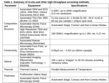
[image:3.595.64.517.181.527.2]High throughput analysis techniques specifically adapted to the characterisation of the structure and composition of thin film materials are required in order to rationalise measured trends in key figures of merit. For the chalcogenide materials synthesised in our programme, a number of methods have been selected in order to provide structural, compositional, optical, thermal and conductivity characterisation; details are given in table 1.
Table 1. Summary of in-situ and other high throughput screening methods.
Parameter Equipment Specifications
Automated SEM and EDS (JEOL JSM-5910; Oxford Instruments INCA 300)
0-30kV, up to 300K magnification (3.0 nm resolution)
Automated Thin Film XRD (Bruker C2 XRD)
Cu Kα source (λ= 1.54184 Å) 2Θ - 29.4° to 62.4° 60 sec per sample (~100µm spot size)
Automated Atomic Force
Microscopy (Oriel) Automated Stage, Contact and Non-Contact Modes. High Resolution TEM and
EDS (JEOL JEM 3010; Oxford Instruments INCA 100TEM)
100-300kV; magnification up to 1.5M, res. 0.21 nm Composition
and Structure
Automated Raman Microscopy (Renishaw)
Conductivity
Automated Four-Point or van de Pauw .
(Four Dimensions Inc. Model 280DI)
0.05µΩ cm – 5 KΩ cm (50nm sample).
Optical
Automated Imaging Ellipsometer
(Nanofilm Technology I-Elli2000)
100 ∆ and ψ ”images” in 20-25 minutes providing refractive index.
Thermal Thermal Camera Parallel Measurement of Temperature
Profilometer (Alpha Step) Thickness
Automated Atomic Force
Electrical Resistivity Measurements
A sample covering a broad composition range was chosen for electrical sheet resistance measurements. Figure 3 shows the ternary diagram for the system with the EDS data points indicating the compositional range covered by the deposition.
[image:4.595.196.397.145.319.2]The as-deposited sample’s conductivity was measured before and after heating in an evacuated oven at 150°C for 2 hours. Each of the points describes the composition where the four-point-probe sheet resistance measurements were made. Figure 4 shows conductivity data, plotted on the ternary diagram, before and after annealing. It should be noted that the scale for this data is Log10. This data can now be correlated against XRD and Raman studies to analyze areas of the ternary system which show properties desirable for electrical phase change data storage.
[image:4.595.71.530.468.640.2]Figure 3: Ternary Diagram Showing the EDS measurements where sheet resistance were made.
Figure 4: Ternary Plots showing the 4-point probe sheet resistivity measurements of the as-deposited film and
after annealing at 150°c
150°c
X Data
2 4 6 8 10
Y D a ta 2 4 6 8 10 26 28 30 32 34 Delta/degrees
2 4 6 8 10
Y D a ta 2 4 6 8 10 144 146 148 150 152
A key problem with the well characterised Ge2Sb2Te5 is its inherent low resistivity in the crystalline phase; large currents are required to Joule heat the material to its melting point. When compared with XRD data these conductivity measurements may reveal areas of the ternary system which show high crystalline sheet resistivity. It is known that moving away from the Ge2Sb2Te5 composition severely affects the set operation of any potential non-volatile memory devices. It is possible that doping this area of the ternary may decrease the switching speed of the system without affecting its electrical properties.
Multilevel or grey scale memories have been suggested as a possible mechanism of increasing the capacity of phase change memory devices. For electrical, phase change, grey scale, RAM a large phase resistivity range is desirable. The conductivity ternary plots of Figure 4 reveal the compositions of greatest change in resistivity between the as-deposited and 150°c anne aled Ge:Sb:Te compositions. It is also believed that the switching speed of this area of the ternary could also be decreased by doping.
Optical Characterization
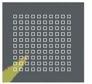
Crystalline regions of the as-deposited films were visible by eye. A processed image of a sample is presented in figure 5. The lighter, more reflective, crystalline regions are clear. To further explore these reflectivity differences, an automated imaging ellipsometer was used to scan 100 “images” in 20-25 minutes providing refractive index and absorption measurements across the sample.
[image:5.595.203.352.307.444.2]Figure 6 shows the results of the ellipsometric measurement of ∆ and Ψ (degrees) measured for the 100 fields shown in the sample in figure 5 plotted in the form of a contour map. The ellipsometric angle ∆ primarily reflects the difference in thickness of the material, which can be substantiated by comparison with the thickness data from AFM (Figure 4). The ellipsometric angle Ψ is dominated by the absorbance of the phase. Comparison of the map of Ψ with the processed optical image clearly shows the correlation of Ψ with the highly reflecting crystalline phase
[image:5.595.68.444.569.722.2]Figure 5: Digitally processed image of a typical as-deposited Ge:Sb:Te film
Figure 6: Ellipsometric
measurements of ∆ and
Conclusions
High throughput techniques allow fast deposition and screening of chalcogenide alloys. To efficiently investigate the optical and electrical data storage capability throughout the available compositional space fast deposition and methodologies are required. Adding dopents to phase change materials adds yet anther degree of flexibility and controllability of the resultant film properties. High throughput synthesis and
screening are ideal tools for the discovery of new phase change materials. Such techniques have now been applied to the deposition of Ge:Sb:Te thin films. Rapid primary electrical and optical measurements of compositions spanning the entire ternary system have been possible.
Acknowledgements
The authors acknowledge the technical and scientific support of Mark Light (EPSRC X-Ray Facility), Claire Mormiche (Ilika technology - AFM), John Tetteh (Ilika Technology - Informatics), Duncan Smith (Chemistry Graduate Student), Sebastian Powers (Chemistry/Ilika Placement Student) and Majid Hassan (ORC – Thin Film Engineering).
References
[1] Materials aspects in phase change optical recording, Zhou, Materials Science and Engineering A, 304– 306 (2001) 73–80
[2] Xiang, X.-D., et al., Science (1995) 268, 1738
[3] Characterization of Ge–Sb–Te thin films deposited using a composition spread approach, Kyrsta, S, et al, Thin Solid Films 398-399 (2001) 379-384
[4] Application of High Throughput Methods to the Development of Materials For Non-Magnetic Storage, C. Eric Ramberg, et al, Mat. Res. Soc. Symp. Proc. Vol. 803