ISSN(Online) : 2319-8753 ISSN (Print) : 2347-6710
I
nternational
J
ournal of
I
nnovative
R
esearch in
S
cience,
E
ngineering and
T
echnology
(An ISO 3297: 2007 Certified Organization)
Vol. 5, Issue 4, April 2016
Characterization of Single and Double Gate
InSb Based HEMT Devices for High
Frequency Application
R.Saravanakumar 1, A.Sarathi2, C.Ramesh3
Associate Professor, Department of Electronics and Communication Engineering, SKP Engineering College
Tiruvannamalai, Tamilnadu, India1
Assistant Professor, Department of Electronics and Communication Engineering, SKP Engineering College
Tiruvannamalai, Tamilnadu, India2
Professor, Department of Electronics and Communication Engineering, SKP Engineering CollegeTiruvannamalai,
Tamilnadu, India 3
ABSTRACT: We report the implementation of double gate symmetric Metal Oxide Semiconductor HEMT(DG-MOSHEMT) based on AlInSb/InSb material .The DG-MOSHEMT consist of 30nm gate length and it exhibit high
transconductance (Gm) , high cut off frequency (ft)and maximum drain bias. We achieved greater ft=750 GHz and fmax
=950 GHz this result is higher than single gate AlInSb/InSb MOSHEMT. The High Electron Mobility Transistor (HEMT) is an important device for high speed, high frequency and microwave circuits.
KEYWORDS: IndiumAntimonide, MOSHEMT, symmetric MOSHEMT
I .INTRODUCTION
The Sb-based devices have intrinsic advantage of high speed and low power consumption that can provide the technology required for these application. In III-V narrow band gap semiconductors such as InAs andInSb have showed extremely high electron mobility because of their smallelectron effective mass [table1], which has brought about an increasing interest in themselves as promising channel materials for future logic, communication and terahertz devices. The two-dimensional electron gascreated at the interface between the channel and the barrierlayers of High Electron Mobility Transistors (HEMT) provides a high concentration of electrons in the channelwith very high mobility. In AlInSb/InSbparticularly suitable for low-drain voltage operation,this material reduced DC-power consumption than GaAs. In Metal oxide Semiconductor HEMT(MOSHEMT) with insulating dielectrical are widely investigated, and excellent performance utilizing Al2O3, TiO2, HfO2.In AlInSb/InSb MOSHEMT using Al2O3 as gate
dielectric.
In symmetrical High electron mobility transistor the drain current(Id) and transconductance (gm) is high. In
single gate High mobility electron transistor the short channel effect is high than compare to double gate. In double gate
MOSHEMTin order to improve higher values of the transconductance over drain conduction ratio gm/gd and lower gate
ISSN(Online) : 2319-8753 ISSN (Print) : 2347-6710
I
nternational
J
ournal of
I
nnovative
R
esearch in
S
cience,
E
ngineering and
T
echnology
(An ISO 3297: 2007 Certified Organization)
Vol. 5, Issue 4, April 2016
GaAs InGaAs InAs InSb units
Energy gap 1.43 0.75 0.356 0.175 eV
Electorn effective
mass 0.072 0.041 0.027 0.013 eV
Mobility for pure material
8500 14,000 30,000 78,000 cm2 V-1 s-1
Electron
saturation velocity 1.2*10 7 8*10 8 3*10 7 5*10 7 cm s-1
Intrinsic carrier
concentration 1.1*10 7 5*10 11 1.3*10 15 1.9*10
16 cm -3
Electron free
mean path length 80 108 194 226 nm
Table[1] comparison of III-IV semiconductor materials
II. DEVICE STRUCTURE
ISSN(Online) : 2319-8753 ISSN (Print) : 2347-6710
I
nternational
J
ournal of
I
nnovative
R
esearch in
S
cience,
E
ngineering and
T
echnology
(An ISO 3297: 2007 Certified Organization)
Vol. 5, Issue 4, April 2016
(b)
Figure1:(a) & (b) Schematic diagram of single gate &double gate symmetric MOSHEMT based on AlInSb/InSb
In Figure1 shows the schematic illustration of the device geometry. In single gate symmetric MOSHEMT grown on 100nm SiC substrate.The barrier1/barrier2 are Al0.15In0.85Sb with 14nm/15nm dimensions. The donor sheet
density of the -doping layer is constant as 2.0*1012 cm2.An etchstop layer placed above the -doping layer with 5nm
for the purpose of controlling the threshold voltage. The source/drain are fabricated in metal with 50nm length and
70nm height. The distance of Lsg and Lgd are 5nm .The Oxide layer(Al2O3) placed below the gate with 3nm thickness.
In double gate symmetric MOSHEMT barrier3/barrier4 are grown below the channel with 14nm/15nm dimensions.
III . RESULTS AND DISCUSSIONS
In Figure2, shows the Vg and Idat source to gate voltage at 0.5V for single and double gate symmetric MOSHEMT.
From this plot the double gate drain current (Id) is higher than compare to single gate symmetric MOSHEMT. In Figure
3,shows the Vg and Gm for Vgs at 0.5V. In double gate symmetric MOSHEMT achieve greater transconductance (Gm)
than compare to single gate MOSHEMT. The Al0.15In0.85Sb
Barrier/buffer, the electron distribution into the barrier as source to gate voltage increases, because of shallower quantum well (QW) channel.
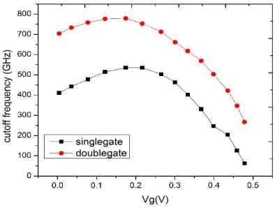
In fig4, which shows the measurement of cut off frequency(fT) versus gate voltage. At drain voltage 0.5V, anfT of
500GHz for single gate MOSHEMT and 750 GHz for double gate symmetric MOSHEMT. From fig 5, shows the
AlInSb/InSb device shows the maximum oscillation frequency (fmax) at drain voltage 0.5V. The estimated fmaxin InSb
ISSN(Online) : 2319-8753 ISSN (Print) : 2347-6710
I
nternational
J
ournal of
I
nnovative
R
esearch in
S
cience,
E
ngineering and
T
echnology
(An ISO 3297: 2007 Certified Organization)
Vol. 5, Issue 4, April 2016
Figure 2 , Vg and Id as a function of Vgs at 0.5 V for single & double gate symmetric MOSHEMT .
Figure 3, Vg and Gm function of Vgs at 0.5V for single & double gate symmetric MOSHEMT.
ISSN(Online) : 2319-8753 ISSN (Print) : 2347-6710
I
nternational
J
ournal of
I
nnovative
R
esearch in
S
cience,
E
ngineering and
T
echnology
(An ISO 3297: 2007 Certified Organization)
Vol. 5, Issue 4, April 2016
Figure5, maximum oscillation frequency versus gate voltage for single & double gate MOSHEMT.
(a) (b)
Figure6 : plot (a) and (b) shows the Id versus Vds characteristics of single & double gate MOSHEMT.
From fig 6, shows the InSb channel show Id versus Vds characteristics with Lg 30nm for single & double gate
MOSHEMT at drain voltage 0.5 V. The gate voltage varies from -1.0 V to 1.0 V the corresponding drain current (Id)
increased in mA/mm. In this graph, the double gate MOSHEMT reaches the high drain current than single gate
symmetric MOSHEMT. The device exhibits excellent pinch-off and drain current saturation behavior up to Vd = 0.7 V.
In fig 7,shows the Vg and Gm for different gate length at 0.5 V for single gate MOSHEMT. The different gate length
the transconductance (Gm) increased. From the plot the different gate length are 120nm,60nm and 30nm the
ISSN(Online) : 2319-8753 ISSN (Print) : 2347-6710
I
nternational
J
ournal of
I
nnovative
R
esearch in
S
cience,
E
ngineering and
T
echnology
(An ISO 3297: 2007 Certified Organization)
Vol. 5, Issue 4, April 2016
Figure 7, Vgversus Gm for different gate length at 0.5 V for single gate MOSHEMT.
Figure 8, Vg and Gm for different gate length double gate MOSHEMT.
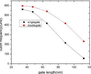
From fig 9, shows cutoff frequencies (fT) versus different gate length in nm at drain voltage at 0.5V. In different gate
length the cutoff frequencies are increased. From the plot the different gate length are 120nm, 90nm, 70nm, and 30nm the corresponding cutoff frequencies are 100GHz, 200GHz, 400GHz and 550GHz respectively. From the relation
ft=Gm/Cox the transconductance (Gm) increased it leads to high cutoff frequencies.
ISSN(Online) : 2319-8753 ISSN (Print) : 2347-6710
I
nternational
J
ournal of
I
nnovative
R
esearch in
S
cience,
E
ngineering and
T
echnology
(An ISO 3297: 2007 Certified Organization)
Vol. 5, Issue 4, April 2016
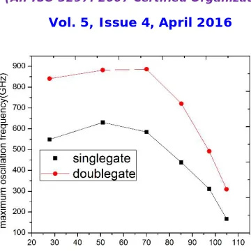
Figure 10, maximum oscillation frequency versus gatelength in nm at drain voltage 0.5V for single and double gate MOSHEMT.
In fig10, the fmaxversus Vg at drain voltage 0.5 V for single and double gate symmetric MOSHEMT. In single gate the
different gate length are 30nm, 70nm, 100nm and 110nm the corresponding fmax are 550GHz, 500GHz, 350GHz,
100GHz respectively. In double gate MOSHEMT the gatelength are reduced the frequencies are increased. The different gate length are 110nm, 100nm, 70nm, 30nm the corresponding frequencies values are 300GHz, 550GHz, 800GHz, 850GHz respectively.
IV. CONCLUSION
We have demonstrated InSb quantum well transistors down to 30nm gatelength with comparable high frequency performance to today’s Si MOSFET’s. The device exhibit excellent transfer and output characteristics to extract current voltage curves. Frequency analysis predicted a cutoff frequency fT = 750GHz and a maximum oscillation
frequency fmax = 950GHz for double gate symmetric MOSHEMT. In future work, according to Moore’s law requires
continuous scaling of Si MOSFETs. The physical gatelength of Si – transistors that are utilized is about 100nm. It is expected that critical dimension will reach about 10nm in the future to improve the transfer, output and RF characteristics of these devices to improve the high performance with low power.
REFERENCES
[1] S. Dattaet al., “85nm Gate Length Enhancement and Depletion mode InSb Quantum Well Transistors for Ultra High Speed and Very Low Power Digital Logic Applications,” 2005 IEEE IEDM Tech. Dig., pp. 763-766, 2005.
[2] Dae-Hyun Kim et al., “fT = 688 GHz and fmax = 800 GHz in Lg = 40 nm In0.7Ga0.3As MHEMTs with gm_max> 2.7 mS/μm,” 2011 IEEE IEDM. Tech. Dig., pp. 13.6.1-13.6.4, 2011.
[3] H. Nishino et al., “Monte Carlo Study of Strain Effect on High Field Electron Transport in InAs and InSb,” 2010 IPRM Proceedings, pp. 156-159. 2010. [4] F. Machida et al., “Strain Effects on Performances in InAs HEMTs,” 2011 IPRM Proceedings, pp. 437-440. 2011.
[5] S. Hara et al., “Quantum-Corrected Monte Carlo Simulation of InSb HEMTs Considering Strain Effects,” 2011 TWHM Abstracts, p. 41, 2011. [6] H. I. Fujishiroet al., “Quantum Corrected Monte Carlo Analysis of Scaling Behavior of Nano-Scale InGaAs High Electron Mobility Transistors,” 2007 ISCS Abstracts, pp. 2795- 2798, 2007.
[7] D.-H.Kim and J.A.del Alamo, IEEE Electron Device Lett.,Vol.29, pp.830-833, 2008.
[8] T.Takegishi, H.Watanabe, R.Yamada, T.Matumoto, S.Haraand H.I.Fujishiro, in Proc. IPRM, pp.124-127, 2009. [9] Y.Hori, Y.Ando, Y.Miyamoto, and O.Sugino, Solid State Electronics, vol.43, pp.1813-1816, 1999.
[10] T.Mizuno, S.Takagi, N.Sugiyama, H.Satake, A.Kurobe, and A.Toriumi, IEEE Electron Device Lett., Vol.21, pp.230-232, 2000. [11] K.Brennan and K.Hess, Solid State Electronics, vol.27, pp.347-357, 1984.
[12] D.C.Herbert, P.A.Childs, Richard A.Abram, G.C.Crow, and M.Walmsley, IEEE Trans. on Electron Devices, vol. 52, pp.1072-1078, 2005. [13] H.Rodilla, T.Gonzalez, D.Pardo, and J.Mateos, J.Appl. Phys., vol. 105, pp.1-6, 2009.
[14] V.Chandramouli and C.M.Maziar, Solid State Electronics, vol.36, pp285-290, 1993. [15] S.C.Jain, J.R.Willis, and R.Bullough, Adv. Phys. 39, pp.127-190, 1990.
[16] M.L.Cohen and T.K.Bergstresser, Phys. Rev., vol.141, pp. 789-796, 1966. [17]M.M.Rieger and P.Vogl, Phys. Rev. B, vol. 48, pp. 14276-14287, 1993.