A Systematic Study on Chip and Package Co-Design of
Clock Network
Sandeep Singh& Neeraj Gupta
1M.Tech. Student, 2Assistant Professor, Dept. of Electronics & Communication Engineering
Amity University Haryana, Gurugram, India
Abstract: -The Package chip mounted on a
printed wiring board. It increase the integration level of system, therefore we are able to work with smaller sizes that are the main advantage of Chip and Package Network. It is an organic or ceramic substrate, and then increases the number of layers to handle this signal and power delivery to get a high efficiency &high performance. The field of packaging has been driven by the number of input output connections required to a chip. So we saw
traditionally that quadruple flat
packagecould not fulfill the I/O
requirements in future. So moving towards ball grid array packageswhich enable a higher number of I/O. So this flip chip ball grid array package can support up to 1000 input-output connections.
I INTRODUCTION
The require going to this next evolution in terms of chip packaging. The 3D technology enables significant reduction in the interconnects and it is improve the overall system performance. So now the timeline of evolution of this different packaging technology. Pentiums used to use these pin grid array package where 2D array of pins which would fit into our motherboard. If we look at the various hierarchy products
thatwe have seen, fortunately there has been very close integration, environmental aspects in production has to be taken care of and time to volume has been volume time has been drastically reduced. The thing about portable products, everybody wants to make their product thinner, smaller, but they still want a lot of function in it. A lot of the chip scale packages that are very thin, low profile.
Let the example of smart phone. It has put together all the different chip size packages, and we notice that there’s a lot of different constructions. We can have a lot of different type substrates. Maybe a flex circuit, a rigid substrate. It could be mostly laminate, but it could have some lead frame types, as well. A lot of different structures, but they’re all called chip-sized packages. These lots of different products on that Mobil phone board and basically used to package a lot of different devices whether it’s Flash, ASICs. Controllers, DSP, Processors Analog Devices. Many of the analog devices and in the ultimate chip scale package would be a wafer level package which is basically what we call a WLP. Those are basically the same size as the dye itself, just with bumps on it.
The chip package could be either ceramic or plastic and then things got a little more complicated, where we introduced all these various packages. That is still using lead frames. But mostly it was a lead frame type package,as shown in Fig. 1&2. These structures called laminated substrates instead of just a lead frame to put this stuff on. Higher pin counts, things got a little more complex. And then all the way up they started getting even more complex. So, basically surmise it to say that the complexity in the packaging has grown over time and still continues to grow.
Figure 1 Motherboard chip package.
These things called DIP packages, as on figure, even though they’ve been around a really long time we progressed all the way to a TSOP and these acronyms are kind of thrown around a lot. TSOP i.e. Thin Small Outline Packages, the TSOP, have gone into this era which we call the area array package.
We have things like ball grid array, CSP, stack packages everybody wants to go high, more dense on the board so that the only way to go in up. So we got third dimensional packages. Ultimate package being a wafer-level package, which is no package at all.
Figure 2Chip Package
III PACKAGE: The area array package is
basically its call a Ball Grid Array and mostly it could be a plastic or laminate substrate. It could be a ceramic substrate. It could be tape or flex although we don’t see much of those anymore because of the expense and the lack of infrastructure in that but these packages is pretty much found on a lot of products today, whether it’s a laptop or portable product and they basically look like they’re shown here[7].
If we look at the construction of this typically the plastic ball grid array, or PBGA, has a laminate substrate. Some kind of epoxy mold compound on the top part.
they kind of freaked out because they couldn’t see these things [7].
Figure 3flip chip package for motherboard.
This is a typical motherboardas shown in Fig. 3. This just happens to be an old Intel motherboard with a package and we can see that package would fit on this board. This is a flip chip package.
We can see the exposed die, there’s no lid on this so this die has been mounted onto the board. These are very common in all of processor packages, or something like that would have a package like that flip chip.
A. Flip Chip:-
Flip chip is basically a bump on a die and we can have all kinds of different types of bumps,as shown in Fig. 4.
Figure 4Layout of Flip-chip Technology
A very common term it’ll hear used is C4. C4 stands for controlled collapse chip connection. That’s kind of a long word, and when IBM invented that term, secretaries had to type it up, and that was too long to type. So they shortened it to just call it C4 and, they will use that general term to refer to a flip chip. Mostly it’s a high temperature solder bump in the early days, a eutectic low temperature solder bump. In some cases when it’s a high temperature solder to a laminate there would be some solder put on the board and then it would be attached. Also polymer bumps that could be used. There is also an isotropic conductive film that could be used. There is also some, other conductive adhesives that can be used. But the majority is typically been the solder bump, as shown in Fig. 5[11].
Some of the drivers for this growth in the flip chip technology; they are very high performance, products. ASICs, field-programmable gate arrays, DSPs, chipsets, graphics, digital TV.Other, like media products, and then a lot of our wireless products, being driven by form factor and performance. A lot of our baseband processors moving to flip chip, and I’ll talk about this thing called the package-on-package, or PoP, and that is an application processor moving to flip chip,
If we look at what one of these things basically looks like, die sizes, or it can be up to, say, 25 millimeters, on a side. The input outputs counts up to thousands. Minimum bump pitch somewhere probably a 130 micron is probably where we are today very small bump diameters, bump heights of 100 micron being typical and a fairly thin package from point four to point seven five millimeters, mostly laminate substrates here with some ceramics and here is a pictures to show what these things looks like in the past. This is actually a flip chip device that is mounted on a module [8].
First IBM flip chip was a copper ball as the “bump” in 1960s. Widespread adoption of the high-Pp. bump using evaporation process (C4 bump). Industry moved to electroplated bumps for flip chip Intel, IBM, Motorola etc. as shown in Fig. 6.
Industry moving to copper pillar process, Transition started with Intel, now all industry made is Cu pillar.
Figure6Die Bump / Flip Chip Microwave Technology (DBD)
The industry is now in the process of moving to something new which is called a copper pillar, a copper post. The difference being that on this post that we have now, there’ll be a little bit of a cap. That is solder and that will be connected [10]. So basically, Intel started this transition. With the presser processor. Now if we look at any Intel part, they’ll all be a copper pillar with some solder cap on it. And by 2013, 2014, we expect this type of technology for flip chip bump to move into very high volume production[8].
B. Chip Size Package (CSP):-
The new iPhone we looked at one of these boards, we would find a lot of CSPs in it. Chip scale or chip size packages and we notice that this is not much space on this board. It’s all crammed full. So the introduction of chip size package is really what enabled a lot of our portable products. Because it allowed us, to package the die in something almost the same size as the die and to crack, cram it all on that board and we know so this really is the era of the chip scale package that we’re in today.
Figure 7Ball grid array (BGA) Chip Size Package
This as we can see is very low profile because there is no package around it. This is the package itself. The die and the package are the same. So all we’ve done is basically taken pieces of silicon and we’ve put solder balls on that and then we’ve attached that to the board. So we can see that this obviously is much thinner than anything that has a substrate on it in a package and obviously, if we use the flex circuit piece it can be fairly thin.So, if we want a really, really thin product is almost package less. But we are still having a ability to all those bump fabrication in the form of wafer-level package. So, this is an example of one of
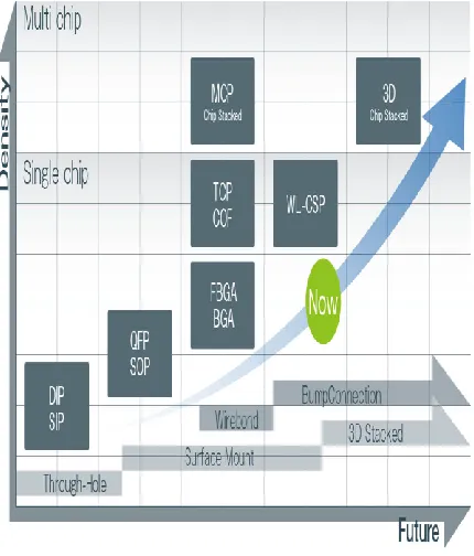
these lead frame type packages we’ll see that they’re pads not balls on it but it’s still called a chip skill package.The Chip Package Roadmapshown in Fig. 10 so it is shows that the day to day technology grows.
Figure 8Chip Package Roadmap
C. Wafer-Level Packages(WLP):-
parts are fabricated on this. It’s an increasing number of analog devices being packaged this way. These are the solder bumps that are formed on the top of it[7].
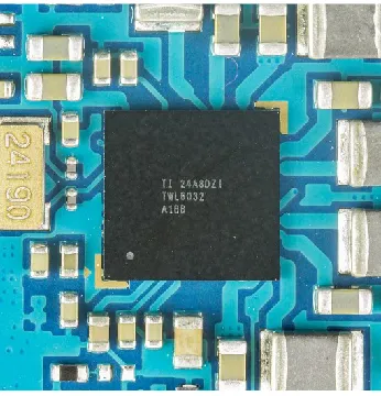
Figure 9Wafer-level packages Texas
Instruments TWL6032.This is one of the highest ones that we’ve seen but these are down at point four millimeters pitch. We are seeing things done at point three millimeter pitch in the future so these balls are getting tighter and tighter, the distance between them all is. This is the use in power management also. RF wireless LAN, integrated passive devices, LED drivers, sound chips, all these things that we find in phones.
Figure 10Wafer-level packages
D. 3D Packaging:-
Now, it’s an ultra-thin, ultra-compact package, as shown in Fig. 11.so if we putting, just stacking down on top of each other little bumps to connect them, that obviously is the best solution. This is demonstrator device that Samsung put together a long time ago. These are basically they could be, they are stacked-up die. This is actually a stacked die with wire bonds. This is from Samsung. This is probably flash memory we can also this is an edge connection for Levine sensors on a on a stacking them here. This is vertical circuits. We could see the edge connection here. Basically used in a lot of space applications, military applications, a very interesting technology and then we have also a type of package [2].
Figure 11High-density 3D Semiconductor Package
E. Basic structure for 3D IC:
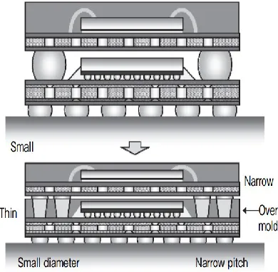
It’s basically taking die and stacking them together to give us the thinnest possible structure,as shown in Fig. 12&13.
Top of each other with this connecting with this pump. Typically, we’re use a process. Use a laser, but most are using familiar with in this, in the fab side and this via like five to 30 microns but that’s going to be, we’re going to put a bump on this. Things and connect these chip together once. Wafer about 50 microns thin [3].
Chips that close together solvers out interconnect delay problems. Our bandwidth bottleneck, it solves the problem device latency. It solves a lot of power management issues because which we put things together they’ll have lower power in it. When we go through some of the charts but there are a lot of issues before we can go and do this in high volume manufacturing
issues including EDA tool availability, a manufacturing process that have very high yield, the thermal part, gee I’m stacking logic and memory, the memory has an operating temperature of which it can’t exceed. If we put a logic device on it, and its hot what happens to my memory. It gets hot, so we have to have a thermal solution.
Smart phones we’d find a lot of 3d packaging. We would see some of these stacked memory parts. There would be some cases where as I mentioned have a flip chip on the bottom on the stack on the top and these package on packages that I mentioned here. In this case we can see that there’s multiple memory die on the top package, a logic die on the bottom and that’s all that’s in the digital base bin section [5].
Figure 123D TSV package technologies
So these different 3D packages inside our smartphone today.In 1980 many Japanese
companies, research institutes and
universities had extensive works on 3D ICs. Unfortunately, they were all failed. Since then, many works on 3D IC have been done. However, all these works did or are doing the same mistakes. Technically, it is not possible to optimize various transistors at below 400 degree Celsius [2].
IV CHIP EMBEDED MEMORY:-
Memory is the functional blocks in most high performance logic products. More embedded memory is better for high performance because embedded memory is about 10x faster than off-chip memory, as shown in Fig. 14Chip Embedded Memory.
Embedded memory is about 100x more expensive than off chip memory. Where 100x comes from cell density difference between embedded SRAM and off-chip DRAM, and product price difference between CPU and off-chip Dram. Embedded memory could reduce power consumption up to 75% in the memory sub-system because no I/0 is needed between CPU and off-chip memory. Embedded flash will be crucial portion of internet-of-things for large data storage, fast data access, low power consumption, security updated, and small form factor
Smart phone, Laptop or our tablet device to reduce this interconnect length and also to reduce form factor, the only way to do that is to stack these chips, either on top or side by side. So there are two ways to could do it. We could either stack, in a 3D manner
which is more, revolutionary approach. A more evolutionary approach which is currently in production now in using stacking. If we’re talking about the Mobil phone space. We got that phone. It gets hot sometimes. The battery doesn’t last long enough but if we go to something we call a wide IO, it would, where we stack the memory and the logic together and connect with those little bumps and the through silicon, we would have a lot thinner smaller form factor product. It would solve our problem with the memory band width and improve the memory the memory power efficiency, which is what we really want. We really have performance and form factor drivers to get this technology moved into production.
Stacked DRAM, with through silicon via in as terms of samples, and things like that with a lot of programs announced by Hynix, Micron, Samsung over here, is the only people that have been able to deliver some of these memory in production today, for some specific government programs. This cube concept has actually a controller in there as well, so as soon as we figure out how to stack that these are some of the early stacking that elide showed.
V ALTERNATIVES TO 3D IC WITH TSV:-
If we just took part of that stuff, and we put it on the silicon interposer and we had the die communication with each other through the interposer. So they’re not stacked on top of each other, but they’re really pretty close together. So if we did that, we could call that a 2.5D solution and we’d have interposers in the with through-silicon via in it. So there are some advantages in this. We can use the silicon to handle the stress for the large die with the ultra-low-k dielectrics. We could incorporate some integrated passives in there too[5].
This is the package substrate and laminate substrate. This is the die, and this FPGA is partitioned into four die and these are mounted on the silicon interposer of carrier and then they are attached to the laminate substrate. So people that are doing this, Xilinx is already shipping this part. Altera’s announced something with it. There are a lot of ASIC designs by many companies.
This is Xilinx, and it is call stacked silicon interconnect. So here’s this idea of this
interposer. Now this die, this FPGA, has now been a partitioned design so that we’ve divided the die instead of this one big honking die where send the signal across it, we’ve partitioned this into four slices. These slices are fabricated at 28 Nano meter node technology and then we can bend these. So basically select the good ones, they’re bumped, and then we’re going to put them on this interposer that has the through-silicon via, and redistribution layers, so that these chips are going to communicate right here. Side by side, they’re going to communicate through this interposer to each other. So they’re going to act as a function of like, one big die and then this silicon interposer is going to place on this package substrate. And there’s via connecting here. So this is a ball grid array package. Remember we stated out with ball grid array package structure. But it’s multiple die. But it’s still a three dimensional structure. But it actually functions as if it were a single device. So these things, here are the micro bumps, as I mentioned, where we’re accessing power and ground, logic regions and basically, we can see the little bumps right there, and then these are we can see that these are connected [8].
this is passive interposer process is basically an older technology so it’s 65 nanometer generation node technology and it has four metal layer’s on it. A redistribution layer’s on it. These are side by side, we could just put a heat sink on the top and not have to worry about and a lot of power sitting on top of each other as if they were stacked die[2].
VI CONCLUTIONS:-
The first generation of, this was using these wire bonds. These wire bonds connecting with chip on silicon package and solder balls which would then connect this package to the outside world. Now in currently we have micro-bump technology which is connecting directly with silicon to this package
The second thing which is driving this change is now improvement in the system performance which is enabled by going to this 2.5D or 3D Packages. So there’s this term which is frequently used called the memory wall. So the overall system performance is limited by the bandwidth at which our CPU can communicate with the system memory.
A lot of structures that have been fabricated and prototypes, and a lot of processes that are still needed to be worked on for us to get the yield up to really see that technology going to large scale production. There’s a lot applications that are using through silicon via, image sensors in MEMs[5].
Various 3D-IC integration technologies are applied for high performance, of low cost applications. Mobile, Wearable in consumer applications will drive the TSV-less 3D
integration technologies such as fan-out WLP to mass production, to reduce cost and power consumption. Cloud Data server, and high performance computing for deep learning will drive through-silicon visa (TSVs)based heterogeneous integration,
including silicon photonics. Fully
integrated/automated co-design between die interposer and package are needed, not only in implementation optimization, but also thermal, electrical analysis and many other fields.
REFERENCES
[1] M.Lakshmanan, AlauddinMohd Ali, "High Performance Parallel Multiplier Using Wallace-Booth Algorithm," IEEE International Conference on Semiconductor Electronics,2002, pp. 433-436
[2] X. Zhao, J. Minz, and S. K. Lim, “Low-power and reliable clock network design for through-silicon via (TSV) based 3D ICs,” Trans. CPMT, vol. 1, no. 2, pp. 247–259, 2011.
[3] S. Garg and D. Marculescu, “Mitigating the impact of process variation on the
performance of 3-D integrated circuits,” Trans. VLSI, vol. 21, no. 10, pp.
1903–1914, 2013.
136–149, 2015.
[5] L.-R. Huang et al., “Parametric fault testing and performance characterization of post-bond interposer wires in 2.5-D ICs,” Trans. CAD, vol. 33, no. 3, pp.
476–488, 2014.
[6] L. Cederström, “EDA environments for 3D chip stacks,” in 3D Stacked Chips – From Emerging Processes to Heterogeneous Systems, I. A. M. Elfadel and G. Fettweis, Eds. Springer, 2016, ch. 9.
[7] UMC, “0.13μm flip-chip layout guideline,” p. 6, 2004.
[8] C.-Y Peng, W.-C Chao, Y.-W. Chang, and J.-H Wang, “Simultaneous
block and I/O buffer floorplanning for flip-chip design,” Proc. of ASPDAC,
[9] G. Huang, D. Sekar, A. Naeemi, K. Shakeri, and J. D. Meindl, “Compact PhysicalModels for Power Supply Noise and
Chip/Package Co-Design of
GigascaleIntegration”, Electronic
Component and Technology Conference, Reno, June,2007.
[10] Van Zant, Peter (2000). Microchip Fabrication. New York: McGraw-Hill.
[11] Desmond Y.R. Chong, “Development of a New Improved High Performance Flip
Chip BGA
![Figure 5One-Piece Lid High Performance Flip Chip BGA (HPfcBGA) Package[11].](https://thumb-us.123doks.com/thumbv2/123dok_us/1995718.1264190/3.612.325.589.431.665/figure-piece-high-performance-flip-chip-hpfcbga-package.webp)