VLSI Architecture for Exploiting Carry-Save Arithmetic
Using Verilog HDL
Saritha Gone
& Dr. G.V. Maha Lakshmi
1PG Scholar, Department. of ECE, Sreenidhi Institute of Science & Technology ,Yamnampet,
Ghatkesar, Medchal, Telangana.
2Professor, Department of ECE, Sreenidhi Institute of Science & Technology ,Yamnampet,
Ghatkesar, Medchal, Telangana.
Abstract: The selective use of carry-save arithmetic, where appropriate, can accelerate a variety of arithmetic-dominated circuits. Carry-save arithmetic occurs naturally in a variety of DSP applications, and further opportunities to exploit it can be exposed through systematic data flow transformations that can be applied by a hardware compiler. Field-programmable gate arrays (FPGAs), however, are not particularly well suited to carry-save arithmetic. To address this concern, we introduce the “field programmable counter array” (FPCA), an accelerator for carry-save arithmetic intended for integration into an FPGA as an alternative to DSP blocks. In addition to multiplication and multiply accumulation, the FPCA can accelerate more general carry-save operations, such as multi-input addition (e.g., add integers) and multipliers that have been fused with other adders. Our experiments show that the FPCA accelerates a wide variety of applications than DSP blocks and improves performance, area utilization, and energy consumption compared with soft FPGA logic. The extension for the
above project is Dadda Multiplier.
Experimental results are seen by using Xilinx ISE 13.2.
Index Terms—Carry-save arithmetic, field-programmable gate array (FPGA), Arithmetic optimizations, flexible accelerator.
I. INTRODUCTION
Modern embedded systems target high-end application domains requiring efficient
implementations of computationally intensive digital signal processing (DSP) functions. The
incorporation of heterogeneity through
specialized hardware accelerators improves performance and reduces energy consumption [1]. Although application-specific integrated circuits (ASICs) form the ideal acceleration solution in terms of performance and power, their inflexibility leads to increased silicon complexity, as multiple instantiated ASICs are needed to accelerate various kernels. Many researchers have propounded the use of
domain-specific coarse-grained reconfigurable
accelerators in order to increase ASICs‘ flexibility without significantly compromising their performance.
High-performance flexible data paths have been propounded to efficiently map primitive or chained operations found in the initial data-flow graph (DFG) of a kernel. The templates of complex chained operations are either extracted directly from the kernel‘s DFG or specified in a predefined behavioral template library. Design decisions on the accelerator‘s data path highly impact its efficiency. Existing works on coarse-grained reconfigurable data
paths mainly exploit architecture-level
optimizations, e.g., increased instruction-level
parallelism (ILP). The domain-specific
computation of entire sub expressions using multiple ALUs with heterogeneous arithmetic features.
The aforementioned reconfigurable architectures exclude arithmetic optimizations during the architectural synthesis and consider them only at the internal circuit structure of primitive components, e.g., adders, during the logic synthesis . However, research activities have shown that the arithmetic optimizations at higher abstraction levels than the structural circuit one significantly impact on the data path
performance. In [10], timing-driven
optimizations based on carry-save (CS) arithmetic were performed at the post-Register Transfer Level (RTL) design stage. In [11], common sub expression elimination in CS computations is used to optimize linear DSP
circuits. Verma et al. [12] developed
transformation techniques on the application‘s DFG to maximize the use of CS arithmetic prior
the actual data path synthesis. The
aforementioned CS optimization approaches target inflexible data path, i.e., ASIC,
implementations. Recently, a flexible
architecture combining the ILP and pipelining techniques with the CS-aware operation chaining has been aimed. However, all the aforementioned solutions feature an inherent limitation, i.e., CS optimization is bounded to merging only additions/subtractions. A CS to binary conversion is inserted before each operation that differs from addition/subtraction, e.g. multiplication, thus, allocating multiple CS to binary conversions that heavily degrades performance due to time-consuming carry propagations.
In this brief, we propose a high-performance architectural scheme for the synthesis of flexible hardware DSP accelerators by combining optimization techniques from both the architecture and arithmetic levels of abstraction. We introduce a flexible data path architecture that exploits CS optimized templates of chained operations. The aimed
architecture comprises flexible computational units (FCUs), which enable the execution of a large set of operation templates found in DSP kernels. The accelerator architecture delivers average gains in area-delay product and in energy consumption compared to state-of-art flexible data paths , sustaining efficiency toward scaled technologies.
II. PREVIOUS WORK
[1] Hardware acceleration has been proved an extremely promising implementation strategy for the digital signal processing (DSP) domain. Rather than adopting a monolithic application-specific integrated circuit design approach, in this brief, we present a novel accelerator architecture comprising flexible computational units that support the execution of a large set of operation templates found in DSP kernels. We differentiate from previous works on flexible accelerators by enabling computations to be aggressively performed with carry-save (CS) formatted data. Advanced arithmetic design concepts, i.e., recoding
techniques, are utilized enabling CS
optimizations to be performed in a larger scope than in previous approaches. Extensive experimental evaluations show that the accelerator architecture delivers average gains of up to 61.91% in area-delay product and 54.43% in energy consumption compared with the state-of-art flexible data-paths.
cycle is enough for producing the correct result in the majority of the cases. In this paper our proposal takes advantage of multispeculation in order to increase the performance of tree structures with a negligible area penalty. By judiciously introducing these structures into computation trees, it will only be necessary to predict the carry signals in certain selected nodes, thus minimizing the total number of predictions and the number of operations that can potentially mispredict. Hence, the average latency will be diminished and thus performance will be increased.
[3] The selective use of carry-save arithmetic, where appropriate, can accelerate a variety of arithmetic-dominated circuits. Carry-save arithmetic occurs naturally in a variety of DSP applications, and further opportunities to exploit it can be exposed through systematic data flow transformations that can be applied by a hardware compiler. Field-programmable gate arrays (FPGAs), however, are not particularly well suited to carry-save arithmetic. To address this concern, we introduce the ―field programmable counter array‖ (FPCA), an accelerator for carry-save arithmetic intended for integration into an FPGA alternative to DSP blocks. In addition to multiplication and multiply accumulation, the FPCA can accelerate more general carry-save operations, such as multi-input addition (e.g., add K>2 integers) and multipliers that have been fused with other adders. Our experiments show that the FPCA accelerates a wider variety of applications than DSP blocks and improves performance, area utilization, and energy consumption compared
with soft FPGA logic
.
One of the ways that custom instruction set extensions can improve over software execution is through the use of hardware structures that have been optimized at the arithmetic level. Arithmetic hardware, in many cases, can be partitioned into networks of full-adders, separated by other logic that is better expressed using other types of logic gates. In this paper we present a novel logic synthesis
technique that optimizes networks of full adders and is intended for use in the context of custom instruction set synthesis. Unlike earlier work (e.g., Three Greedy Approach) our approach does not require any prior knowledge about the functionality of the circuit. The aimed technique automatically infers the use of carry-save arithmetic, when appropriate, and suppresses its use when unfavorable. Our approach reduces the critical path delay through networks of full adders, when compared to the Three Greedy Approach, and in some cases, reduces the cell area as well.
On the exemplary vehicle of a Viterbi decoder as frequently used in communication systems we show which costs in terms of ATE
complexity arise implementing typical
components on different types of architecture blocks. A factor of about seven orders of magnitude spans between a physically
optimized implementation and an
implementation on a programmable DSP kernel. An implementation on an embedded FPGA kernel is in between these two representing an attractive compromise with high flexibility and low power consumption. Extending this comparison to further components, it is shown quantitatively that the cost ratio between different implementation alternatives is closely related to the operation to be performed. This information is essential for the appropriate partitioning of heterogeneous systems.
III. Carry-Save Arithmetic: Motivational Observations and Limitations
built from networks of FAs and HAs. The most common way of computing a multi-input addition is through compressor tree introduced by Wallace and Dadda. A compressor tree takes a set of n integers and reduces them to two output values sum (S) and carry (C).
CS representation has been widely used to design fast arithmetic circuits due to its inherent advantage of eliminating the large
carry-propagation chains. CS arithmetic
optimizations rearrange the application‘s DFG and reveal multiple input additive operations (i.e., chained additions in the initial DFG), which can be mapped onto CS compressors. The goal is to maximize the range that a CS computation is performed within the DFG. However, whenever a multiplication node is interleaved in the DFG, either a CS to binary conversion is invoked or the DFG is transformed using the distributive property. Thus, the aforementioned CS optimization approaches have limited impact on DFGs dominated by multiplications, e.g., filtering DSP applications.
In this brief, we tackle the
aforementioned limitation by exploiting the CS to modified Booth (MB) recoding each time a multiplication needs to be performed within a CS-optimized data path. Thus, the computations throughout the multiplications are processed using CS arithmetic and the operations in the targeted data path are carried out without using any intermediate carry-propagate adder for CS
to binary conversion, thus improving
performance.
IV. Flexible Accelerator
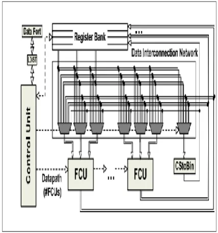
The flexible accelerator architecture is shown in Fig. 1. Each FCU operates directly on CS operands and produces data in the same form1 for direct reuse of intermediate results. Each FCU operates on 16-bit operands. Such a bit-length is adequate for the most DSP data paths, but the architectural concept of the FCU
can be straightforwardly adapted for smaller or larger bit-lengths. The number of FCUs is determined at design time based on the ILP and area constraints imposed by the designer. The CStoBin module is a ripple-carry adder and converts the CS form to the two‘s complement one.
The register bank consists of scratch registers and is used for storing intermediate results and sharing operands among the FCUs. Different DSP kernels (i.e., different register allocation and data communication patterns per kernel) can be mapped onto the proposed architecture using post-RTL data path interconnection sharing techniques.
The control unit drives the overall
architecture (i.e., communication between the data port and the register bank, configuration words of the FCUs and selection signals for the multiplexers) in each clock cycle.
Fig. 1. Abstract form of the flexible data path
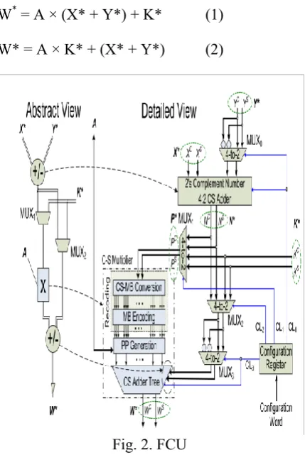
A. Structure of the Flexible Computational Unit
configured to any of the T1–T5 operation templates shown in Fig. 3. The FCU enables intra template operation chaining by fusing the
additions performed before/after the
multiplication &performs any partial operation template of the following complex operations:
W* = A × (X* + Y*) + K* (1)
W* = A × K* + (X* + Y*) (2)
Fig. 2. FCU
The following relation holds for all CS data: X* = { XC, XS} = XC + XS. The operand A is a two‘s complement number. The alternative execution paths in each FCU are specified after properly setting the control signals of the multiplexers MUX1 and MUX2 (Fig. 2). The multiplexer MUX0 outputs Y* when CL0 = 0 (i.e., X* + Y* is carried out) or Y* when X* − Y* is required and CL0 = 1. The two‘s complement 4:2 CS adder produces the N* = X* + Y* when the input carry equals 0 or the N* = X* − Y* when the input carry equals 1. The MUX1 determines if N* (1) or K* (2) is multiplied with A. The MUX2 specifies if K* (1) or N* (2) is added with the multiplication product. The multiplexer MUX3 accepts the output of MUX2 and its 1‘s complement and
outputs the former one when an addition with the multiplication product is required (i.e., CL3 = 0) or the later one when a subtraction is carried out (i.e., CL3 = 1). The 1-bit ace for the subtraction is added in the CS adder tree.
The multiplier comprises a CS-to-MB module, which adopts a recently designed technique to recode the 17-bit P* in its respective MB digits with minimal carry propagation. The multiplier‘s product consists of 17 bits. The multiplier includes a compensation method for reducing the error imposed at the product‘s accuracy by the truncation technique. However, since all the FCU inputs consist of 16 bits and provided that there are no overflows, the 16 most significant bits of the 17-bit W* (i.e., the output of the Carry-Save Adder (CSA) tree, and thus, of the FCU) are inserted in the appropriate FCU when requested.
B. DFG Mapping Onto the FCU-Based Architecture
In order to efficiently map DSP kernels
onto the FCU-based accelerator, the
semiautomatic synthesis methodology has been adapted. At first, a CS-aware transformation is performed onto the original DFG, merging nodes of multiple chained additions/subtractions to 4:2 compressors. A pattern generation on the transformed DFG clusters the CS nodes with the multiplication operations to form FCU template operations (Fig. 3). The designer selects the FCU operations covering the DFG for minimized latency. Given that the number of
FCUs is fixed, a resource-constrained
scheduling is considered with the available FCUs and CStoBin modules determining the resource constraint set. The clustered DFG is scheduled, so that each FCU operation is assigned to a specific control step. A list-based scheduler has been adopted considering the mobility2 of FCU operations. The FCU
operations are scheduled according to
operations are bound onto FCU instances and proper configuration bits are generated. After completing register allocation, a FSM is generated in order to implement the control unit of the overall architecture.
(A) (B)
Fig.3. Typical chaining of addition–
multiplication–addition operations reflecting T1 template of Fig. 3. Its design is based on (A)
CS optimizations with multiplication
distribution (B) incorporating the CS-to-MB recoding concept.
V. EXTENSION
The Dadda multiplier is a hardware multiplier design, invented by computer scientist Luigi Dadda in 1965. It is slightly faster (for all operand sizes) and requires fewer gates (for all but the smallest operand sizes) than array multiplier. Dadda multipliers have the same 3 steps: 1. Multiply (that is - AND) each bit of one of the arguments, by each bit of the other, yielding N2 results. Depending on position of the multiplied bits, the wires carry different weights, for example wire of bit carrying result of a2b3 is 32. 2. Reduce the number of partial products to two layers of full and half adders. 3. Group the wires in two
numbers, and add them with a conventional adder.
Dadda multipliers perform few
reductions only when compared to Wallace multiplier. Because of this, Dadda multipliers have less expensive reduction phase, but the numbers may be a few bits longer, thus requiring slightly bigger adders To achieve this, the structure of the second step is governed by slightly more complex rules than in the wallace multipliers. The reduction rules however are as follows: Take any 3 wires with the same weights and input them into a full adder. The result will be an output wire of the same weight and an output wire with a higher weight for each 3 input wires. If there are 2 wires of the same weight left, and the current number of output wires with that weight is equal to 2 (modulo 3), input them into a half adder. Otherwise, pass them through to the next layer.
If there is just 1 wire left, connect it to the next layer. This step does only as many adds as necessary, so that the number of output weights stays close to a multiple of 3, which is the ideal number of weights when using full adders as (3, 2) counters.
The multiplication of an M-bit multiplicand by an N-bit multiplier yields an N by M matrix of partial products. The reduction of this partial product matrix through the parallel application of (3, 2) and (2, 2) counters results in a matrix with a height of two. Each (3, 2) counter (full adder) accepts three inputs from a given column and produces a sum bit which remains in that column and a carry bit which goes into the next more significant column. A (2, 2) counter (half adder) accepts two inputs from a column and produces a sum bit in the same column and a carry bit in the next more significant column. The implemented 16 × 16 Dadda multiplier with the help of dot diagram is shown in Fig 2 (The notation is taken from [8][10] in which the outputs from a full adder are joined by a solid line, and those from half adders are joined by a line with a dash through the centre). The Dadda scheme essentially minimizes the number of adder stages required to perform the summation of the partial products. This is achieved by using full and half adders to reduce the number of rows in the matrix of bits at each summation stage by a factor of 3/2.
Fig.4 Dadda Multiplier
VI. SIMULATION RESULTS
FCU Simulation.
Design Utilization Summary.
Extension Simulation.
Design Utilization Summary.
VII. CONCLUSION
multiplicative operations. The flexible accelerator architecture is able to operate on both conventional two‘s complement and CS-formatted data operands, thus enabling high degrees of computational density to be achieved. Theoretical and experimental analyses have shown that the solution forms an efficient design tradeoff point delivering optimized latency/area and energy implementations. The extension for the above project is Dadda Multiplier. Experimental results are seen by using Xilinx ISE 13.2. Results when compared with the extension are more better with the flexible accelerator.
Future Scope.
The project here is done for operation in which a number is either multiplied or added. In the Future this can be extended for a polynomial equation which is used in Elliptical Curve Cryptography ECC in which the multiplication process is done for a polynomial equation.
REFERENCES
[1] Kostas Tsoumanis, Sotirios Xydis, GeorgiosZervakis, and Kiamal Pekmestzi‖
Flexible DSP Accelerator Architecture
Exploiting Carry-Save Arithmetic‖.
[2] P. Ienne and R. Leupers, Customizable Embedded Processors: Design Technologies and Applications. San Francisco, CA, USA: Morgan Kaufmann, 2007.
[3] P. M. Heysters, G. J. M. Smit, and E. Molenkamp, ―A flexible and energy-efficient coarse-grained reconfigurable architecture for mobile systems,‖ J. Supercomput., vol. 26, no. 3, pp. 283–308, 2003.
[4] B. Mei, S. Vernalde, D. Verkest, H. D. Man, and R. Lauwereins, ―ADRES: An architecture with tightly coupled VLIW processor and coarse-grained reconfigurable matrix,‖ in Proc. 13th Int. Conf. Field Program. Logic Appl., vol. 2778. 2003, pp. 61–70.
[5] M. D. Galanis, G. Theodoridis, S. Tragoudas, and C. E. Goutis, ―A
high-performance data path for synthesizing DSP kernels,‖ IEEE Trans. Comput.-Aided Design Integr. Circuits Syst., vol. 25, no. 6, pp. 1154– 1162, Jun. 2006.
[6] K. Compton and S. Hauck, ―Automatic design of reconfigurable domainspecific flexible cores,‖ IEEE Trans. Very Large Scale Integr. (VLSI) Syst., vol. 16, no. 5, pp. 493–503, May 2008.
[7] S. Xydis, G. Economakos, and K. Pekmestzi,
―Designing coarse-grain reconfigurable
architectures by inlining flexibility into custom arithmetic data-paths,―Integr., VLSI J., vol. 42, no. 4, pp. 486–503, Sep. 2009.
[8] S. Xydis, G. Economakos, D. Soudris, and K. Pekmestzi, ―High performance and area efficient flexible DSP datapath synthesis,‖ IEEE Trans. Very Large Scale Integr. (VLSI) Syst., vol. 19, no. 3, pp. 429–442, Mar. 2011.
[9] G. Ansaloni, P. Bonzini, and L. Pozzi, ―EGRA: A coarse grained reconfigurable
architectural template,‖ IEEE Trans. Very Large
Scale Integr. (VLSI) Syst., vol. 19, no. 6, pp. 1062–1074, Jun. 2011.
[10] M. Stojilovic, D. Novo, L. Saranovac, P. Brisk, and P. Ienne, ―Selective flexibility:
Creating domain-specific reconfigurable
arrays,‖ IEEE Trans. Comput.-Aided Design
Integr. Circuits Syst., vol. 32, no. 5, pp. 681– 694, May 2013.
[11] T. Kim and J. Um, ―A practical approach to the synthesis of arithmetic circuits using carry-save-adders,‖ IEEE Trans. Comput.- Aided Design Integr. Circuits Syst., vol. 19, no. 5, pp. 615–624, May 2000.