Nonlinear Characteristics of P-I-N Diode Circuits Analyzed
by a Physically Based Simulation Method
Hao Wang1, *, Guodong Wang1, Xiaolian Liu1, Ke Xu2, and Xing Chen2
Abstract—Nonlinear characteristics of semiconductor devices play a key role in the performances of circuits, but their modelling is still a big challenge in circuit simulations nowadays. This paper explores modelling nonlinear characteristics of circuits containing semiconductor devices by presenting a modified physically based simulation method. A p-i-n diode microstrip circuit is taken as a sample, and its nonlinear characteristics, such as the power limiting, bistability, and forward recovery characteristics, are simulated and analysed. The applied method demonstrates its good capability and accuracy of modelling the nonlinear characteristics in the simulation, and moreover clarifies the underlying physical mechanisms. In contrast, the Advanced Design System (ADS) software, a popular circuit simulation program based on the equivalent circuit model, fails to reveal some of those nonlinear characteristics.
1. INTRODUCTION
Semiconductor devices are key components in modern electronic circuits [1, 2]. Their nonlinear characteristics are essential for circuit performances, and thus the accurate modelling of those nonlinear behaviours in circuits is fundamental to the circuit design and application. A number of simulation methods have been proposed, e.g., the equivalent-model based simulation method [3–7]; the analytical-model based simulation method [8], etc.. However, the aforementioned approaches suffer from limitations that may preclude their application in some cases. For example, the equivalent or analytical models may lose their accuracy in some special cases such as high-power or high-frequency applications, and moreover, most of them lack a direct physical interpretation for the physical phenomena. Therefore, nowadays, the simulation of nonlinear characteristics for distributed circuits containing semiconductor devices is still a great challenge.
Among the available techniques, the physically based simulation method attracts researchers’ interest most particularly for the statistical significance and predictive ability [9–11]. It is based on semiconductor devices’ physical models, and solves field equations such as the Maxwell’s equations and semiconductor transport equations, to model the electromagnetic wave propagation and charge transport inside semiconductor devices. Hence it is naturally able to accurately simulate semiconductor devices under various conditions and convenient for predicting the physical effects.
In our previous works, a novel physically based simulation method was proposed for the first time [12, 13]. As an extension of previous studies, the proposed method is modified to be able to model distributed structures by introducing a circuit-field co-simulation model. This paper explores applying this modified physically based simulation method to model semiconductor devices’ nonlinear characteristics in microstrip circuits and clarify the underlying physical mechanisms. Similar to that in our previous works, a commercial p-i-n diode with model number mot bal99lt1 is taken as a sample, and a series of experiments are conducted to validate the simulation results.
Received 5 January 2017, Accepted 20 April 2017, Scheduled 6 May 2017
* Corresponding author: Hao Wang ([email protected]).
1 School of Physics and Electronic Information Engineering, Henan Polytechnic University, Jiaozuo 454000, P. R. China.2 College
∂t q ∂p
∂t = −
1
q∇ ·
− →
Jp−R (3)
− →
Jn = qDn∇n+qµnn∇φ (4)
− →
Jp = qDp∇p+qµpp∇φ (5)
I = A (−→
Jc+−→Jd )
·−→δ =A (
− →
Jn+−→Jp+ε ∂−→E
∂t )
·−→δ (6)
where ε is the permittivity; q is the electron charge, Nt is the net doping concentration; φ is the electrostatic potential; n and p are the electron and hole densities; −→Jn and −→Jp are the electron and
hole current densities;DnandDpare the corresponding diffusion coefficients;µnandµp are the electron
and hole mobilities;I is the branch current;A is the cross-sectional area;−→δ is a unit vector normal to the cross-section.
The procedure of solving the above Equations (1)–(6) can be simplified to the solution of an increment equation
A∆y(k−1)+B∆y(k)+C∆y(k+1)=H(k) (7)
where y = [φ n p]T, ∆y = [∆φ ∆n ∆p]T, A,B, and Care 3×3 matrices, H is a 3×1 matrix. The deriving and solving of Equation (7) is well described in the Reference [12] and need not be detailed here.
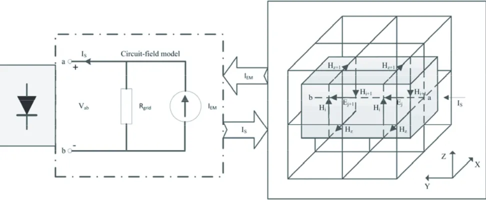
For a two-terminal semiconductor device, the branch current is obtained by calculating Equation (7) for an applied voltageV by Newton’s method. Thus the terminal current can be represented byI(V(t)). For circuits working at high frequencies, they may contain not only lumped elements but also some distributed structures such as microstrip lines. In this paper, the coupling algorithm for semiconductor devices and distributed structures is realized by the circuit-field co-simulation model [15]. Figure 1 illustrates this model for the interaction between a diode and its external distributed part. As shown in the right side of the figure, the distributed part is described by the finite-difference time-domain (FDTD) technique with spatial domain discretized as Yee cell. Assuming a diode is located in the grid at nodes a and b, the external distributed structure can be modelled as an equivalent sub-circuit consisting of a resistor Rgrid and a current source IEM. After solving the lumped circuit at the centrepiece of the
figure, the diode current, in return, is fed back to the field FDTD iteration formulation by IS. The values of the equivalent resistor and current source are determined by Equations (8)–(12) [15].
(
Iyn+1)EM =
β∑=jb
β=ja
(δαβ)Kyijkn+1/(Rny+1)grid (8)
(
Rny+1)grid =
β∑=jb
β=ja
(δαβ) Γnyijk+1/(δx·δz) (9)
Kyijkn+1 = Γnyijk+1·LHSyn+1/2/(δx·δz) + Γnyijk+1(ε˜ijk/δtn+1−σ˜ijk/2 )
Figure 1. Illustration of the circuit-field model for coupling the external distributed structure with a diode.
Γnyijk+1 = 1/(εijk/δt˜ n+1+ ˜σijk/2) (11)
LHSyn+1/2 =
(
Hxijkn+1/2−Hxijkn+1−/21 )
·δxi− (
Hzijkn+1/2−Hzin+1−1/jk2 )
·δzk (12)
3. THE SIMULATION OF NONLINEAR CHARACTERISTICS OF A MICROSTRIP P-I-N DIODE CIRCUIT AND DISCUSSION
In this section, some nonlinear characteristics of a microstrip p-i-n diode circuit will be analysed. The chosen mot bal99lt1 diode and its physical model are illustrated in Figure 2. A Genetic Algorithm (GA) based curve-fitting approach, which is introduced in detail in our previous works [12, 13], is adopted for the extraction of the physical parameters. The extracted results are as follows: the donor and acceptor surface concentrations are 1.8×1016cm−3with a Gaussian doping profile to the interior of the diode; the doping level of i-layer is 0.5×1010cm−3; the widths of the three layers are Xa = 5µm, Xb= 1.55µm and Xd= 0.5µm respectively; the cross-sectional area of the diode isA= 0.7×10⁻⁴cm2.
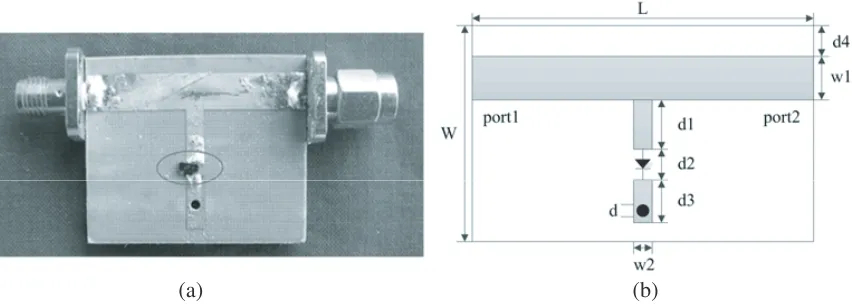
A microstrip p-i-n diode circuit (see Figure 3) is fabricated. It consists of two microstrip lines connected together on Teflon substrate with relative dielectric constant εr = 2.65 and thickness
(a) (b)
(a) (b)
Figure 3. (a) Photo and (b) schematic plot of the microstrip diode circuit.
h = 2 mm. One of the microstrip lines is connected to SMA connectors at both ends. The other microstrip line has a gap,d2, of width 1.35 mm with one end grounded through via hole. A mot bal99lt1 p-i-n diode is mounted across the gap. Other geometrical parameters are as follows (unit mm): L= 32.4,
W = 28.3, w1 = 5.4,w2 = 2.7,d= 1,d1=d3 = 8.1, andd4 = 2.7.
3.1. The Power Limiting and Bistability Characteristics
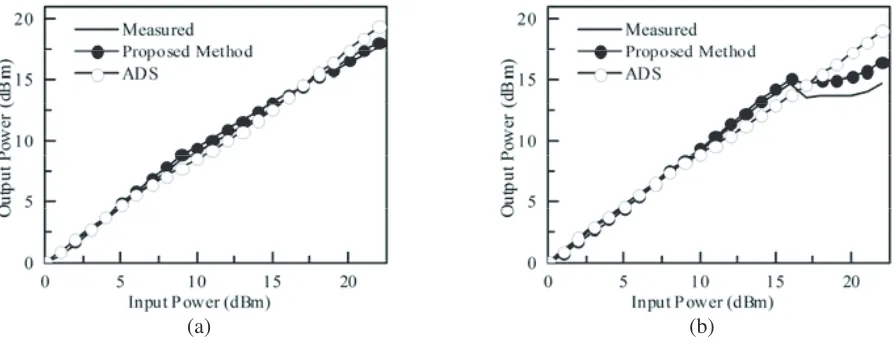
The microstrip circuit, shown in Figure 3, functions as a simple diode limiter with a power limiting characteristic. It has two ports. Port 1 is the input port where power is applied, and port 2 is the output port. The output power versus input power for the microstrip circuit at frequencies of 250 and 600 MHz are simulated by the modified physically based simulation method and the ADS respectively, and then compared with that obtained from experiment, as shown in Figure 4. The measurement is performed by using a CETC power meter AV2432 with an Agilent vector signal generator E8267C. In general, the two modelling approaches both predict the power limiting characteristic, which indicates that the simulated output power is lower than the input power. Moreover, one can observe that the simulation results from both modelling approaches agree well with the measurement ones at frequency of 250 MHz. But for the frequency of 600 MHz, the modified simulation method is more accurate than ADS. In that case, an interesting nonlinear phenomenon, named bistability effect [16–18], occurs. As illustrated in Figure 4(b), the output power increases almost linearly with the input power. However, at the input power of about 16 dBm, there is a jump of the output power. This complicated nonlinear property is successfully predicted by the proposed physically based simulation. In contrast, ADS does not possess the capacity of simulating this physical effect.
3.2. The Forward Recovery Characteristics
The forward recovery characteristic of p-i-n diodes refers to the terminal voltage overshoot phenomenon when a diode turns on abruptly under the influence of the external circuit. This characteristic is very important to p-i-n diodes since it affects the diode switching speed significantly.
Figure 5 shows the forward recovery characteristic of the mot bal99lt1 p-i-n diode. As can be seen in this figure, the measured terminal voltage (solid line) is a little larger than the clamping level at some phase of the forward voltage period, which is denoted by an ellipse. The measurement is conducted under the condition that a 15 dBm sine-wave signal with frequency 50 MHz is injected into the port 1 of the microstrip circuit (see Figure 3) while the port 2 is matched. And a Tektronix TDS1012 oscillograph is used for measurement of terminal voltage.
(a) (b)
Figure 4. Output power vs. input power of the microstrip circuit for (a) 250 MHz and (b) 600 MHz.
Figure 5. The measured and simulated terminal voltage waveforms of the chosen p-i-n diode.
Figure 6. The simulated carrier densities at the center of i-layer during a forward voltage period.
Moreover, the forward recovery characteristic of the chosen p-i-n diode can be clearly and intuitively analysed by the physically based simulation. As illustrated in Figure 6, at the beginning of a forward voltage period, the carrier densities inside i-layer is still in low-level, which means that the diode has a high volume resistivity at this stage. Thus the p-i-n diode actually behaves like a capacitor. This makes the terminal voltage increase with the input voltage and finally results in the rise of the carrier densities. However, when the carrier densities insidei-layer increase to 1.0×1015cm−3, the diode would have low impedance. And this makes the terminal voltage drop to the clamping level.
based approach demonstrates a great capacity of accurately revealing devices’ nonlinear properties, and moreover providing clear physical pictures for those properties. The capacity of accurate simulation and providing physical mechanism for the nonlinear characteristics of semiconductor devices in circuits makes this approach a powerful and effective tool for the semiconductor and distributed circuit analysis.
ACKNOWLEDGMENT
This work was supported by Programs of Henan Polytechnic University (No. B2017-57 and No. T2015-3) and National Natural Science foundation of China (Grant No. U1304608).
REFERENCES
1. Garver, R. V., Microwave Diode Control Devices, Artech House, Norwood, 1976. 2. White, J. F., Microwave Semiconductor Engineering, Van Nostrand, New York, 1982.
3. Mantooth, H. A. and J. L. Duliere, “A unified diode model for circuit simulation,” IEEE
Transactions on Power Electronics, Vol. 12, 816–823, 1997.
4. Kung, F. and H. T. Chuah, “Modeling of bipolar junction transistor in FDTD simulation of printed circuit board,”Progress In Electromagnetics Research, Vol. 36, 179–192, 2002.
5. Xiao, S.-Q., B.-Z. Wang, P. Du, and Z. Shao, “An enhanced FDTD model for complex lumped circuits,”Progress In Electromagnetics Research, Vol. 76, 485–495, 2007.
6. Buiatti, G. M., F. Cappelluti, and G. Ghione, “Physics-based PIN diode SPICE model for power-circuit simulation,”IEEE Transactions on Industry Applications, Vol. 43, 911–919, 2007.
7. Lee, F. K. W. and H.-T. Chuah, “A finite-difference time-domain (FDTD) software for simulation of printed circuit board (PCB) assembly,”Progress In Electromagnetics Research, Vol. 50, 299–335, 2005.
8. Bellone, S., F. G. Della, L. F. Albanese, and F. Pezzimenti, “An analytical model of the forward I-V characteristics of 4H-SiC p-i-n diodes valid for a wide range of temperature and current,”IEEE
Transactions on Power Electronics, Vol. 26, 2835–2843, 2011.
9. Ciampolini, P., L. Roselli, G. Stopponi, and R. Sorrentiono, “Global modeling strategies for the analysis of high-frequency integrated circuits,” IEEE Transactions on Microwave Theory and
Techniques, Vol. 47, 950–955, 1999.
10. Grondin, R. O., S. M. El-Ghazaly, and S. Goodnick, “A review of global modeling of charge transport in semiconductors and full-wave electromagnetics,” IEEE Transactions on Microwave
Theory and Techniques, Vol. 47, 817–829, 1999.
11. Tsai, H. P., R. Coccioli, and T. Itoh, “Time domain global modelling of EM propagation in semiconductor using irregular grids,” International Journal of Numerical Modelling: Electronic
Networks, Devices and Fields, Vol. 15, 355–370, 2002.
12. Chen, X., J. Q. Chen, K. Huang, and X. B. Xu, “A circuit simulation method based on physical approach for the analysis of Mot bal99lt1 pin diode circuits,” IEEE Transactions on Electron
13. Chen, J. Q., X. Chen, C. J. Liu, K. Huang, and X. B. Xu, “Analysis of temperature effect on pin diode circuits by a multiphysics and circuit cosimulation algorithm,” IEEE Transactions on
Electron Devices, Vol. 59, 3069–3077, 2012.
14. Sze, S. M.,Physics of Semiconductor Devices, Wiley, New York, 1981.
15. Sui, W. Q., Time-domain Computer Analysis of Nonlinear Hybrid Systems, CRC Press, Florida, 2002.
16. Lebedev, I. V. and N. V. Drozdovskii, “Bistability and electronic hysteresis of the amplitude characteristics of pin-diode structures,” Journal of Communications Technology & Electronics, Vol. 39, 66–73, 1994.
17. Lebedev, I. V., A. S. Shnitnikov, I. V. Dyakov, et al., “Impedance properties of high-frequency pin diodes,”Solid-State Electronics, Vol. 42, 121–128, 1998.