Article
Morphological, Structural and Optical
Characterization of Bottom-Up Growth of Ag-WO
3Core-Shell Nano-Cube Heterostructures
Muhammad A. Imam and Nitin Chopra *
Department of Metallurgical and Materials Engineering, University of Alabama, Tuscaloosa, AL 35487, USA; [email protected]
* Correspondence: [email protected]; Tel.: +1- (205) 348-4153
Abstract: A new class of nano-cube core-shell heterostructures containing Ag coating on the top of WO3 was fabricated. Physical vapor deposition was used to produce WO3 based nano-heterostructures. All kind of wet toxic chemical process was avoided to make the process simple and contaminant free. Sputtering of WO3 and a subsequent thermal annealing process was done to create nano-cubes of WO3. After that, sputtering of Ag was performed to form the Ag-WO3 core-shell nano-heterostructures (CSNH). The CSNHs were characterized using field emission scanning electron microscopy (FESEM), energy dispersive spectroscopy (EDS), X-ray diffraction analysis (XRD) and UV-vis spectroscopy. The morphologies, elemental analysis, interfaces, crystallinity, phases, and chemical compositions were analyzed. The bottom-up growth of WO3 nanocubes was studied using different time periods at 900°C. Ag coating was also studied before and after annealing. Finally, an optical property (band gap) was also analyzed using Tauc plot derive from absorption spectra. The tailoring the band gap of WO3 from ~2.9eV to ~ 2.45 eV was observed while Ag-WO3 CSNH formed.
Keywords: nano-cube; heterostructures; bottom-up growth; electron microscopy; bandgap; Ag-WO3
1. Introduction
In recent years, manipulation and fabrication of oxide-based core-shell heterostructures and the creation of interface among transition metal oxides have presaged the latest era of materials research. It is enabling an exceptionally discrete set of coinciding material properties to be pooled with an escalating degree of experimental control. Transition metal oxides are also known as semiconducting materials having a wide band gap, which can be tuned while being used as heterostructures. To tune the band gap facilitates rapid charge transport [1] and unique photonic[2] properties which are not possible with a single component or similar structures. Transitional metal oxide heterostructures systems have already exhibited such diverse application as a photocatalyst, photodetectors, FET, LED , gas sensor, chemical sensor, super capacitors, solar cells and surface acoustic wave filters [3-7]. To completely utilize these affluence; it is required to comprehend and be able to control the physics on the smallest scales, creating the exploitation of nanoscale heterostructures. Some of these avenues have already been explored for different applications.
they have a distinctive surface, small-size, and quantum effects. Nanostructures based on transitional metal oxide characteristically have a quicker response due to their very high surface-to-volume ratios. Some literature drew attention towards metal oxide heterostructures, for example, ZnO coated with Ag, WO3, Zinc Tin Oxide (ZTO) and CdS for better photocatalytic and gas sensor application. Similarly, CuO/Co3O4 showed better photocatalytic behavior than simple metal oxide (CuO) nanostructures [3, 5, 17, 25-28]. For better chemical sensing and catalysis, CNT coated Ni/NiO core-shell heterostructures were also studied in the literature [26]. Ag-AgBr coated Al2O3 heterostructure was reported for photo-degradation of industrial contaminants [29]. Ag-coated ZnO, WO3, and MnO2 were also explored for photocatalytic applications, better chemical sensor and supercapacitors respectively [7, 25, 27, 28]. Among the various oxides, WO3 has a graphene-like 2D layered structure [30] with wide band gap (~2.8eV) [31]. This limits its optical responsivity in the visible region of the electromagnetic spectrum for photocatalytic application. Hence, bandgap tuning of WO3 is essential since it governs the energy necessary for the generation of electron-hole pairs. Metal particles such as Ag act as localized surface plasmons (LSP), which attribute electromagnetic waves joined to the combined oscillations of electrons[32]. Ag can tailor the band gap of WO3 in such a way that the spectral response of Ag-coated WO3 heterostructures can be extended to the visible region.
Metal oxide heterostructures drew attention due to their low cost and better photocatalytic/sensing behavior than precious materials. It can be synthesized using a wide array of methods including solution synthesis, gas phase growth i.e. physical/chemical vapor deposition (PVD/CVD), flame synthesis, air oxidation. Gas-phase methods, specifically CVD and pulsed laser deposition (PLD), were used to maintain atomic level control of stoichiometric ratio and perfect particular site deposition. Due to their high cost and low throughput, these processes are not accepted widely for general industrial applications. Sputtering deposition, another tradeoff gas phase technique, have been considered because of its potential for assembling heterostructures, comparably lower cost and high throughput than other gas phase methods[33].
Here, we report a new choice of core-shell nano-heterostructures (CSNH) of Ag-coated WO3 (Ag-WO3) CSNH. Physical vapor deposition (PVD) technique (sputtering) is used to obtain a thin layer, and a subsequent thermal annealing process was used to grow the Ag-WO3 CSNH. All traditional hydrothermal processes were avoided to keep the process simple and reduce the use of toxic chemicals. The nanostructures were extensively characterized for their phases, crystal structures, morphologies and elemental analysis. A field effect scanning electron microscope (FESEM) was used to understand the growth mechanism and morphology. Energy dispersive x-ray spectroscopy (EDX) was performed to confirm the elemental analysis. X-ray diffraction analysis was also conducted to comprehend the phase and crystalline properties of the materials. Along with this, UV-vis was evaluated to calculate the band gap energies of Ag-WO3, which is optically more viable than WO3 for photocatalytic application.
2. Materials and Methods
2.1 Materials
Silicon (111) wafers were acquired from IWS (Colfax, CA), Isopropyl alcohol (IPA) from Sigma-Aldrich (St. Louis, MO), and Deionized (DI, 18.1 MΩ·cm) water was obtained using a Barnstead International DI water system (E-pure D4641). Both WO3 and Ag targets (2 in. diameter) were purchased from AJA International (North Situate, MA). PVD was performed using an AJA International (North Situate, MA) Orion 3 sputtering system. Thermal annealing was conducted in a box furnace (GMF-110) purchased from MTI Inc. (Redmond, CA). Hexane was used as a solvent for ultra-sonication which was procured from Sigma-Aldrich (St. Louis, MO).
2.2. Growth of WO3 Nano-cubes
operating condition for 300 nm thin film of growth was maintained in a high base vacuum pressure of 2×10⁻⁷ torr. Sputtering of WO3 was led using RF power source at 50 W, 150 V with 6.54×10⁻³ torr working pressure. On top of that, 25.1 sccm Ar flow rate, and 25 rpm substrate rotation speed was maintained at a deposition rate of 0.2 A°/s recorded by a quartz thickness monitor. After sputtering of WO3 thin film on Si wafer, it was placed in a crucible and air annealed at ~900°C for 180 min, 240 min and 300 min in a box furnace . After thermal annealing, the furnace was then cooled naturally in the air. Approximately, the 2×2 cm2 area of a silicon wafer containing WO3 nanocubes was ultra-sonicated using hexane as a solvent to prepare a solution for UV-vis.
2.3. Sputtering of Ag onto WO3 Nano-cubes
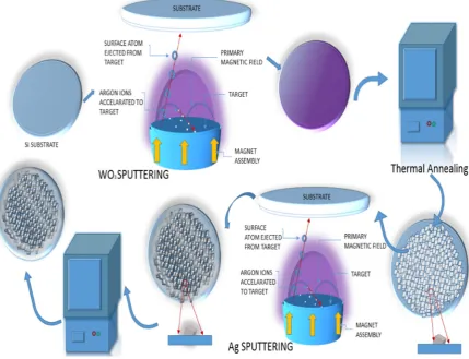
The sample of WO3 nanocubes on Si wafer was loaded into the sputtering chamber. The high base pressure of the chamber was pumped to below 2 × 10− 7 torr. Sputtering of Ag was implemented using a DC power source at 15 W, 750 V with 6.54×10⁻³ torr working pressure. Ar flow rate was maintained 25.1 sccm in the chamber with 25 rpm substrate rotation speed. The sputtering rate was 0.6 A°/s recorded by a quartz thickness monitor. The subsequent heterostructures are stated to as Ag-WO3 core-shell nano-heterostructures (CSNH). Approximately, the 2×2 cm2 area of a silicon wafer containing Ag-WO3 CSNH was ultra-sonicated using hexane as a solvent to prepare a solution for UV-vis before and after 60 min of annealing at inert atmosphere (Ar). The figure, 1 illustrates the schematic fabrication process of CSNH.
2.4. Characterization Methods
A field emission scanning electron microscopy (FESEM, JEOL-7000, equipped with an Oxford EDX detector) was used for morphological characterization and energy-dispersive X-ray spectroscopy (EDX). Philips X`Pert-MPD X-ray Diffraction (XRD) system was used for phase and crystal structure analysis. UV–vis spectroscopy was implemented (absorbance spectra) using an Ocean Optics USB 4000 spectrometer (Dunedin, FL) equipped with DH-2000 UV-vis-NIR light source. The absorption coefficient is defined by the Beer-Lambert’s law as . , where abs and d are the absorption and thickness of the sample holder. Tauc plots were plotted by assuming direct band gap transition and plotting (αhν)1/n vs. hν where n=1/2. The direct band gap were acquired from extrapolating the straight portion of the plot of (αhν)2 versus hν on X- axis at α = 0.
3. Results and Discussion
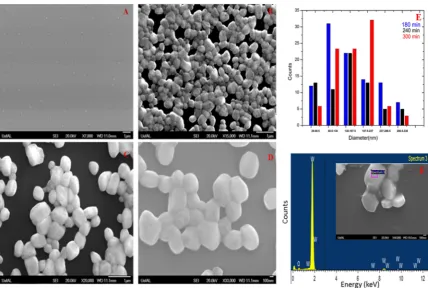
The figure, 2 represents the FESEM micrograph of WO3 after each step including as sputtered (Figure,2A) and after annealing at 900°C for different time periods (Figure,2B-2D). The formation of nano-cube WO3 was evident from the FESEM images (Figure,2B-2D). Thermal process directly enhances the formation of nano-cube WO3 from the sputtered WO3. This is a bottom-up growth of nanoparticles – the vapor-solid (VS) growth mechanism drives this growth process [33]. The diameter of WO3 nanocubes was varied from ~90nm to ~340 nm (Figure, 2E). The figure,2F represents the EDS analysis of growth particle to confirm the elemental analysis. From the spectrum, Tungsten (W) and Oxygen (O2) peak confirm the growth of WO3.
Figure 2. FESEM micrograph of WO3 A. As sputtered, annealing at 900°C B.180 min C.240 min D. 300
min E. Particle size distribution F. EDX based elemental analysis of WO3
Figure 3. FESEM micrograph of Ag-WO3 CSNH A. Before annealing B. Corresponding EDX based
elemental analysis C. After annealing (300°C for 60 min in Ar atmosphere) D. Corresponding EDX based elemental analysis
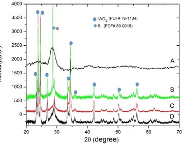
Figure 4. XRD patterns for WO3 A. As sputtered, annealing at 900°C B.300 min C.240 min D. 180 min
Figure 5. XRD patterns of the A. As sputtered WO3, B. Ag-WO3 annealed for 60 min at 300°C, C.
Ag-WO3 before annealing D. Annealed WO3.
The figure, 6 shows the UV-Vis absorption spectra of the WO3 (Figure, 6A), Ag-WO3 before (Figure, 6A) and after (Figure, 6A) annealing. It was observed that there is a lot of changes in major excitation absorption peaks compared to the WO3 (~250 nm) and Ag-WO3 (before ~275 nm and after annealing ~ 280 nm).
Figure 6. UV-vis absorption spectra of WO3 (A), Ag-WO3 before (B) and after annealing (C)
The direct band gap of the CSNH (Figure, 7) was estimated from Tauc plots of hν versus (αhν) 2 for the absorption coefficient α. The band gap of WO3 was calculated ~ 2.9 eV which matched with the literature[31]. The band gap of Ag-WO3 was calculated (Table 1) 2.68 eV and 2.45 eV before and after annealing respectively. The band gap tailoring was identified due to the morphology of CSNH and quantum confinement effect [34]. Interfaces of Ag-WO3 nanocubes heterostructures strongly affects the charge transfer and separation mechanisms[33]. This is due to the Ag nano-layer which is act as a localized surface plasmons (LSP). This separation mechanism attributes the electromagnetic waves to combine the electron oscillations[32]. And this process allows reducing the band gap (Figure, 8.) of the core cell structure. Subsequently, this tailoring band gap permits more visible light interaction with the CSNH than controlled WO3. Tuning the band gap features, the CSNH reflects the promise of this heterostructures as a photocatalysis.
Table 1. Summary of the band gap analysis using UV-vis absorption
Band Gap (eV) Wavelength(nm)
WO3 2.9 428
Ag@WO3 2.68 464
Annealed Ag@WO3 2.45 506
Figure 8. Band gap tailoring mechanism for Ag-coated WO3 CSNH
4. Conclusions
In summary, the study reports the fabrication of core-shell nano-heterostructures. The fabrication comprised of WO3 nano-cubes coated with a thin shell of polycrystalline Ag avoiding all wet chemical routes. Sputtering of WO3 was done on Si substrate, and then the thermal growth of WO3 nanocubes was performed in a box furnace, and again Ag was coated on the surface of the WO3 nanocubes by sputtering. The morphologies, interfaces, elemental analysis, crystal structures, phases and band gaps of the heterostructures were characterized using FESEM, EDX, XRD and UV-vis spectroscopic methods. FESEM images confirmed the particle size, morphologies of the WO3 and the interfaces created between Ag and WO3. EDX supported the elemental analysis of CSNH. On top of that, XRD approved the crystallinity and monoclinic phase of WO3 and presence of polycrystalline Ag coating. In conclusion, band gap analysis of Ag-WO3 nano-cubes heterostructures exposed alterations of absorption peaks compare to pristine WO3 nanocubes and band gap tailoring which could be accredited to the quantum confinement effects of heterostructures.
Acknowledgments: This work was sponsored by the National Science Foundation NSF-EPSCoR RII award (#24067). In addition, N. C. and M.I. thank the Graduate Council Fellowship (GCF) by the University of Alabama Graduate School. The authors express thanks to the Central Analytical Facility (CAF) at the University of Alabama for characterization.
Author Contributions: N. C. and M.I. designed the experiments; M.I. performed the experiments; N. C. and M.I. analyzed the data, M.I. wrote the paper
References
1. Hill, J. J.; Banks, N.; Haller, K.; Orazem, M. E.; Ziegler, K. J., An Interfacial and bulk charge transport model for dye-sensitized solar cells based on photoanodes consisting of core–shell nanowire arrays. Journal of the American Chemical Society 2011, 133, (46), 18663-18672.
2. Musin, R. N.; Wang, X.-Q., Structural and electronic properties of epitaxial core-shell nanowire heterostructures. Physical Review B 2005, 71, (15), 155318.
3. Danwittayakul, S.; Jaisai, M.; Dutta, J., Efficient solar photocatalytic degradation of textile wastewater using ZnO/ZTO composites. Applied Catalysis B: Environmental 2015, 163, 1-8.
4. Eriksson, J.; Khranovskyy, V.; Söderlind, F.; Käll, P.-O.; Yakimova, R.; Spetz, A. L., ZnO nanoparticles or ZnO films: A comparison of the gas sensing capabilities. Sensors and Actuators B: Chemical 2009, 137, (1), 94-102.
5. Lam, S.-M.; Sin, J.-C.; Abdullah, A. Z.; Mohamed, A. R., ZnO nanorods surface-decorated by WO3
nanoparticles for photocatalytic degradation of endocrine disruptors under a compact fluorescent lamp.
Ceramics International 2013, 39, (3), 2343-2352.
6. Tasaltin, C.; Ebeoglu, M. A.; Ozturk, Z. Z., Acoustoelectric effect on the responses of SAW sensors coated with electrospun ZnO nanostructured thin film. Sensors 2012, 12, (9), 12006-12015.
7. Xia, H.; Hong, C.; Shi, X.; Li, B.; Yuan, G.; Yao, Q.; Xie, J., Hierarchical heterostructures of Ag nanoparticles decorated MnO2 nanowires as promising electrodes for supercapacitors. Journal of Materials Chemistry A
2015, 3, (3), 1216-1221.
8. Wang, X.; Liao, M.; Zhong, Y.; Zheng, J. Y.; Tian, W.; Zhai, T.; Zhi, C.; Ma, Y.; Yao, J.; Bando, Y., ZnO Hollow Spheres with Double‐Yolk Egg Structure for High‐Performance Photocatalysts and Photodetectors.
Advanced Materials 2012, 24, (25), 3421-3425.
9. Habibi, M. H.; Habibi, A. H.; Zendehdel, M.; Habibi, M., Dye-sensitized solar cell characteristics of nanocomposite zinc ferrite working electrode: Effect of composite precursors and titania as a blocking layer on photovoltaic performance. Spectrochimica Acta Part A: Molecular and Biomolecular Spectroscopy 2013, 110, 226-232.
10. Han, Z.; Liao, L.; Wu, Y.; Pan, H.; Shen, S.; Chen, J., Synthesis and photocatalytic application of oriented hierarchical ZnO flower-rod architectures. Journal of hazardous materials 2012, 217, 100-106.
11. Habibi, M. H.; Rahmati, M. H., The effect of operational parameters on the photocatalytic degradation of Congo red organic dye using ZnO–CdS core–shell nano-structure coated on glass by Doctor Blade method.
Spectrochimica Acta Part A: Molecular and Biomolecular Spectroscopy 2015, 137, 160-164.
12. Eskizeybek, V.; Sarı, F.; Gülce, H.; Gülce, A.; Avcı, A., Preparation of the new polyaniline/ZnO nanocomposite and its photocatalytic activity for degradation of methylene blue and malachite green dyes under UV and natural sun lights irradiations. Applied Catalysis B: Environmental 2012, 119, 197-206. 13. Habibi, M. H.; Karimi, B.; Zendehdel, M.; Habibi, M., Fabrication, characterization of two nano-composite
CuO–ZnO working electrodes for dye-sensitized solar cell. Spectrochimica Acta Part A: Molecular and Biomolecular Spectroscopy 2013, 116, 374-380.
14. Akhavan, O.; Choobtashani, M.; Ghaderi, E., Protein degradation and RNA efflux of viruses photocatalyzed by graphene–tungsten oxide composite under visible light irradiation. The Journal of Physical Chemistry C 2012, 116, (17), 9653-9659.
15. Habibi, M. H.; Rahmati, M. H., Fabrication and characterization of ZnO@CdS core–shell nanostructure using acetate precursors: XRD, FESEM, DRS, FTIR studies and effects of cadmium ion concentration on band gap. Spectrochimica Acta Part A: Molecular and Biomolecular Spectroscopy 2014, 133, 13-18.
16. Kavitha, T.; Gopalan, A. I.; Lee, K.-P.; Park, S.-Y., Glucose sensing, photocatalytic and antibacterial properties of graphene–ZnO nanoparticle hybrids. Carbon 2012, 50, (8), 2994-3000.
17. Habibi, M. H.; Karimi, B.; Zendehdel, M.; Habibi, M., Preparation of nanostructure mixed copper-zinc oxide via co-precipitation rout for dye-sensitized solar cells: The influence of blocking layer and Co (II)/Co (III) complex redox shuttle. Journal of Industrial and Engineering Chemistry 2014, 20, (4), 1462-1467.
18. Li, Y.; Zhang, W.; Niu, J.; Chen, Y., Mechanism of photogenerated reactive oxygen species and correlation with the antibacterial properties of engineered metal-oxide nanoparticles. ACS nano 2012, 6, (6), 5164-5173. 19. Montazerozohori, M.; Hosseini Pour, S. A., Photocatalytic decolorization of 5-[4-(dimethylamino)
phenylmethylene]-2-thioxo-4-thiazolidinone using nano-powder zinc oxide at various basic buffer pHs.
20. Habibi, M. H.; Mardani, M., Co-precipitation synthesis of nano-composites consists of zinc and tin oxides coatings on glass with enhanced photocatalytic activity on degradation of Reactive Blue 160 KE2B.
Spectrochimica Acta Part A: Molecular and Biomolecular Spectroscopy 2015, 137, 785-789.
21. Penza, M.; Milella, E.; Anisimkin, V., Monitoring of NH3 gas by LB polypyrrole-based SAW sensor. Sensors
and Actuators B: Chemical 1998, 47, (1), 218-224.
22. Jakubik, W. P.; Urbańczyk, M. W.; Kochowski, S.; Bodzenta, J., Palladium and phthalocyanine bilayer films for hydrogen detection in a surface acoustic wave sensor system. Sensors and Actuators B: Chemical 2003, 96, (1), 321-328.
23. Hejczyk, T.; Urbanczyk, M.; Jakubik, W., Semiconductor sensor layer in SAW gas sensors configuration.
Acta Physica Polonica-Series A General Physics 2010, 118, (6), 1153.
24. Jakubik, W. P., Hydrogen gas-sensing with bilayer structures of WO3 and Pd in SAW and electric systems.
Thin Solid Films 2009, 517, (22), 6188-6191.
25. Saoud, K.; Alsoubaihi, R.; Bensalah, N.; Bora, T.; Bertino, M.; Dutta, J., Synthesis of supported silver nano-spheres on zinc oxide nanorods for visible light photocatalytic applications. Materials Research Bulletin 2015, 63, 134-140.
26. Chopra, N.; Shi, W.; Bansal, A., Structural evolution and stability studies of heterostructures comprised of carbon nanotubes decorated with nickel/nickel oxide core/shell nanoparticles. Carbon 2011, 49, (11), 3645-3662.
27. Patil, S. S.; Patil, R. H.; Kale, S. B.; Tamboli, M. S.; Ambekar, J. D.; Gade, W. N.; Kolekar, S. S.; Kale, B. B., Nanostructured microspheres of silver@ zinc oxide: an excellent impeder of bacterial growth and biofilm.
Journal of Nanoparticle Research 2014, 16, (11), 1-11.
28. Xu, L.; Yin, M.-L.; Liu, S., Superior sensor performance from Ag@WO3 core–shell nanostructure. Journal of
Alloys and Compounds 2015, 623, (0), 127-131.
29. Zhou, X.; Hu, C.; Hu, X.; Peng, T.; Qu, J., Plasmon-Assisted Degradation of Toxic Pollutants with Ag−
AgBr/Al2O3 under Visible-Light Irradiation. The Journal of Physical Chemistry C 2010, 114, (6), 2746-2750.
30. Xu, M.; Liang, T.; Shi, M.; Chen, H., Graphene-like two-dimensional materials. Chemical reviews 2013, 113, (5), 3766-3798.
31. Huang, B.-R.; Lin, T.-C.; Liu, Y.-M., WO3/TiO2 core–shell nanostructure for high performance
energy-saving smart windows. Solar Energy Materials and Solar Cells 2015, 133, (0), 32-38.
32. Xu, L.; Yin, M.-L.; Liu, S. F., Agx@WO3 core-shell nanostructure for LSP enhanced chemical sensors.
Scientific reports 2014, 4.
33. Shi, W.; Chopra, N., Controlled fabrication of photoactive copper oxide–cobalt oxide nanowire heterostructures for efficient phenol photodegradation. ACS applied materials & interfaces 2012, 4, (10), 5590-5607.
34. Chopra, N.; Shi, W.; Lattner, A., Fabrication and characterization of copper oxide (CuO)–gold (Au)–titania (TiO2) and copper oxide (CuO)–gold (Au)–indium tin oxide (ITO) nanowire heterostructures. Materials
Characterization 2014, 96, (0), 71-77.