Available Online atwww.ijcsmc.com
International Journal of Computer Science and Mobile Computing
A Monthly Journal of Computer Science and Information Technology
ISSN 2320–088X
IJCSMC, Vol. 3, Issue. 3, March 2014, pg.326 – 331
RESEARCH ARTICLE
Design of Power Gated ML Sensing
Low Power CAM
Neelam Sharma S
M. E VLSI Design
Sri Shakthi Institute of Engineering & technology
[email protected]
Abstract
A Content Addressable Memory (CAM) is a memory unit that performs single clock cycle content matching instead of addresses. CAMs are vast used in look-up table functions, network routers and cache controllers. Since basic lookups are performed over all the stored memory information there is high power dissipation. In reality there is always trade-offs between power consumption, area used and the speed. CAMs are popular in network routers for packet forwarding and packet classification, but they are also beneficial in a variety of other applications that require high speed. The main CAM challenge is to reduce power consumption associated with the large amount of parallel active circuitry, without sacrificing speed or memory density. Thus robust, high-speed and low-power ML sense amplifiers are highly sought after in CAM designs. In this work, we introduce a parity bit and effective gated-power technique to reduce the peak and average power consumption and enhance the robustness of the design against process variations.
Index Terms—CMOS, content addressable memory (CAM), match-line
1.
Introduction
Figure 1. Block diagram of Conventional CAM
This uses two forms of CAM types such as;
1) Pre-Computation CAM Design: The pre -computation CAM uses additional bits to filter some mismatched CAM words before the actual comparison. These extra bits are derived from the data bits and are used as the first comparison stage. For example, in Fig. 2(a) number of “1” in the stored words are counted and kept in the Counting bits segment. When a search operation starts, number of “1”s in the search word is counted and stored to the segment on the left of Fig. 2(a). This extra information is compared first and only those that have the same number of “1”s are turned on in the second sensing stage for further comparison. This scheme reduces a significant amount of power required for data comparison, statistically.
2) Parity Bit Based CAM: The parity bit based CAM design is shown in Fig. 2(b) consisting of the original data segment and an extra one-bit segment, derived from the actual data bits. Only the parity bit is obtained, i.e., odd or even number of “1”s. The obtained parity bit is placed directly to the corresponding word and ML. Thus the new architecture has the same interface as the conventional CAM with one extra bit. During the search operation, there is only one single stage as in conventional CAM. Hence, the use of parity bits does not improve the power performance.
In the case of a matched in the data segment (e.g., ML3), the parity bits of the search and the stored word is the same, thus the overall word returns a match. When 1 mismatch occurs in the data segment (e.g., ML2), numbers of “1”s in the stored and search word must be different by 1. As a result, the corresponding parity bits are different. Therefore now we have two mismatches (one from the parity bit and one from the data bits). If there are two mismatches in the data segment (e.g., ML0, ML1 or ML4), the parity bits are the same and overall we have two mismatches. With more mismatches, we can ignore these cases as they are not crucial cases. The sense amplifier now only has to identify between the 2-mismatch cases and the matched cases.
2.
Gated-Power ML Sense Amplifier Design
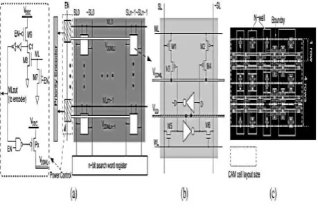
The CAM cells are organized into rows (word) and columns (bit). Each cell has the same number of transistors as the conventional P-type NOR CAM and use a similar ML structure. However, the “COMPARISON” unit, i.e., transistors M1-M4, and the “SRAM” unit, i.e., the cross-coupled inverters, are powered by two separate metal rails, namely VDDML and the V DD, respectively. The VDDML is independently controlled by a power transistor (Px)and a feedback loop that can auto turn-off the ML current to save power.
Figure 2(b) Proposed parity bit based CAM
Figure 3. Proposed power-gated CAM with each CAM cell and its layout
3.
Results and Discussions
SYSTEM SPECIFICATION: MICROWIND version 3.0
Figure 2(a) Conventional pre-computation CAM
The evolution of integrated circuit (IC) fabrication techniques is a unique fact in the history of modern industry. The improvements in terms of speed, density and cost have kept constant for more than 30 years. By the end of 2000, “System-on-Chips” with about 100,000,000 transistors will be fabricated on a single piece of silicon no larger than 2x2 cm.
At logic level, the MOS is considered as a simple switch. Moreover, the logic switch is unidirectional, meaning that the logic signal always flows from the source to the drain. This major restriction has no physical background. In reality, the current may flow both ways. The reason why the logic MOS device enables the signal to propagate only from source to drain is purely a software implementation problem. In the logic simulator of DSCH3, an arrow indicates whether or not the current flows, and its direction. When the device is OFF, the drain keeps its last logic value, thus acting as an elementary memory.
Figure 4.3 Proposed power-gated CAM
The MICROWIND program allows designing and simulating an integrated circuit at physical description level. The package contains a library of common logic and analog ICs to view and simulate. MICROWIND includes all the commands for a mask editor as well as original tools never gathered before in a single module (2D and 3D process view, VERILOG compiler, tutorial on MOS devices). Access to Circuit Simulation by pressing one single key is obtained. The electric extraction of our circuit is automatically performed and the analog simulator produces voltage and current curves immediately.
Figure 4.2 Timing diagram of conventional CAM.
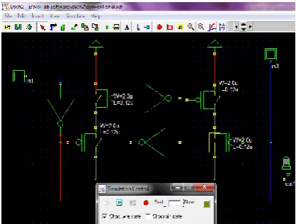
The above figure 4.1 shows the output simulation of conventional CAM loaded in DSCH3. During a pre-charge stage, the MLs are held at ground voltage level while both SL and ~SLs are at VDD. During evaluation stage, complementary search data is broadcast to the SL and ~SLs.
When mismatch occurs in any CAM cell (for example at the first cell of the row D=“1”; ~D= “0”; SL=“1”; ~SL=“0”), transistor on the right will be turned on, charging up the to a higher voltage level. A sense amplifier (MLSA) is used to detect the voltage change on the ML and amplifies it to a full CMOS voltage output. If mismatch happens to none of the cells on a row, no charge up path will be formed and the voltage on the ML will remain unchanged, indicating a match.
The above figure 4.3 shows the proposed power gated ML sensing circuit with parity bit simulation output in DSCH3. The input search data are loaded search data register and broadcast into the memory banks through pairs of complementary search-lines and are directly compared with every bit of the stored words using comparison circuits. The matched output will be shown as the LED glows. If mismatch occurs the output will be zero.
The above figure 4.2 shows voltage vs voltage, voltage vs current, voltage vs time and frequency vs time simulations with different power values.
The steps to compute the results include;
(i)Click File→ Open in the main menu. Select CONV.SCH in the list. In this circuit are one button situated on the left side of the design, the CAM and a led. Click Simulate→ Start simulation in the main menu.
(ii)The schematic diagram including one CAM (CONV.SCH). Now click inside the buttons situated on the left part of the diagram. The result is displayed on the led’s. The red value indicates logic 1; the black value means logic 0. Click the button Stop simulation shown in the picture above. You are back to the editor.
(iii)VERILOG COMPILING: Use DSCH3 to create the schematic diagram of the circuit. Verify the circuit with buttons and lamps. Save the design under the name conv.sch using the command File → Save As.
(iv)Generate the Verilog text by using the command File → Make Verilog File. In MICROWIND3, click on the command Compile → Compile Verilog File. Select the text file conv.txt.
(v) Click Compile. When the compiling is complete, the resulting layout appears shown below. The circuit is routed on the left and on the right. Now, click on Simulate →Start Simulation
(vi)The timing diagrams of figure 4.3 appears and the truth table of the circuit is verified. Click on Close to return to the editor.
4.
Conclusion
We proposed an effective gated-power technique and a parity-bit based architecture that offer several major advantages, namely reduced peak current (and thus IR drop), average power consumption, boosted search speed and improved process variation tolerance. Hence at different supply voltages power consumed in parity bit and power-gating techniques will differ.
References
[1] K. Pagiamtzis and A. Sheikholeslami, “Content-addressable memory (CAM) circuits and architectures: A tutorial and survey,” IEEE J. Solid-State Circuits, vol. 41, no. 3, pp. 712–727, Mar. 2006.
[3] I. Arsovski and A. Sheikholeslami, “A mismatch-dependent power allocation technique for match-line sensing in content-addressable memories,” IEEE J. Solid-State Circuits, vol. 38, no. 11, pp. 1958–1966, Nov. 2003.
[4] pipelined hierarchical search scheme,” IEEE J. Solid-State Circuits, vol. 39, no. 9, pp. 1512–1519, Sep. 2004.
[5] N. Mohan and M. Sachdev, “Low-leakage storage cells for ternary content addressable memories,” IEEE
Trans. Very Large Scale Integr.(VLSI) Syst., vol. 17, no. 5, pp. 604–612, May 2009.
[6] O. Tyshchenko and A. Sheikholeslami, “Match sensing using matchline stability in content addressable memorys (CAM),” IEEE J. Solid-State Circuits, vol. 43, no. 9, pp. 1972–1981, Sep. 2008.
[7] N. Mohan, W. Fung, D. Wright, and M. Sachdev, “A low-power ternary CAM with positive-feedback match-line sense amplifiers,” IEEE Trans. Circuits Syst. I, Reg. Papers, vol. 56, no. 3, pp. 566–573, Mar. 2009. [8] S. Baeg, “Low-power ternary content-addressable memory design using a segmented match line,” IEEE
Trans. Circuits Syst. I, Reg.Papers, vol. 55, no. 6, pp. 1485–1494, Jul. 2008.