48 |
P a g e
DESIGN & SIMULATION OF DVR USING SRFT
Indu Bhushan
1, Abhay Kumar Shah
21
Associate Prof.,
2Assistant Prof., Department of Electrical Engineering,
Greater Noida Institute of Technology, Knowledge Park-II, Greater Noida UP (India)
ABSTRACT
The protection of the sensitive unbalanced nonlinearloads fromsag/swell, distortion, and unbalance in supply
voltage isachieved economically using the dynamic voltage restorer (DVR).A simple generalized algorithm
based on basic synchronousreference-frame theory has been developed for the generation ofinstantaneous
reference compensating voltages for controlling aDVR. This novel algorithm makes use of the d-q transform.
The algorithm is general enoughto handle linear as well as nonlinear loads. A capacitor-supported DVR does
notneed any active power during steady-state operation because theinjected voltage is in quadrature with the
feeder current. The proposedcontrol strategy is validated through extensive simulation.
Index Terms: Dynamic Voltage Restorer (DVR), Srftcontroller, Nonlinear Load, Voltage-Source
Converter (VSC).
I. INTRODUCTION
A DVR is a custom power device used at distribution level .It is similar to SSSC(Static synchronous series
compensator)used at transmission level, but its control and objectives are different from SSSC. The DVR is
implemented using voltage source converter (VSC) with fast switching power semiconductor devices such as
IGBT or IGCT instead of GTO used in SSSC. The voltage injected by VSC in series with distribution feeder is
controlled using sinusoidal PWM control technique. The rapid switching capability provided by IGBT enables
the use of more sophisticated control technique to provide dynamic compensation to sag/swell and harmonics.
A DVR can be viewed as a variable frequency variable voltage source determined by the control algorithm.
The schematic diagram of a self-supported DVR is shown in fig .1.Three phase source voltages (Vsa ,Vsb ,
Vsc) are connected to the 3-phase critical loads through series impedance (Za ,Zb, Zc) and an injection
transformer in each phase. The terminal voltages (Vta,Vtb,Vtc) have power quality problems and the DVR
injects compensating voltages (VCa,VCb,VCc) through an injection transformer to get undistorted and balanced
load voltages (VLa,VLb,VLc) . The DVR is implemented using a voltage source converter (VSC) along with a dc
capacitor (Cdc) . A ripple filter (Lr ,Cr, Rr) is used to filter the switching ripple in the injected voltage. The
considered load, sensitive to power quality problems is a three –phase balanced lagging power factor load.
Various control algorithms are used in implementation of DVR.
The primary objectives of DVR are as follows ,
Dynamic compensation for balanced voltage sags.
Dynamic compensation for balanced voltage swells.
49 |
P a g e
Dynamic compensation for the harmonics present in the supply voltage.
Dynamic compensation for the other power quality problems like surges ,notches present in supply voltage.
II. DESIGN OF DVR
The design of DVR includes selection of rating of the VSC , rating of an injection transformer ,magnitude of DC
bus voltage ,rating of DC bus capacitor and components of ripple filter. The design of component of ripple filter
depends upon the switching frequency of IGBTs of VSC. Value of DC bus capacitor depends on energy
requirement in transient condition .The magnitude of DC bus voltage depends on requirement of worst case sag
compensation, however there is a practical limit(40%) on maximum sag compensation using self/capacitor
supported DVR due to limited energy storage in capacitor depending upon value of capacitance. The ratings of
VSC and injection transformer depend on load current and requirement of worst case sag compensation.
2.1 Selection of Switching Frequency
For selecting a switching frequency ,the highest order of harmonics is considered which has to be compensated
.The switching frequency must be at least two times of highest order of harmonic which is to be compensated
.The selection of switching frequency also highly related to speed of processor as the sampling frequency
depends on the speed of the processor. The general range of the switching frequency is from 5 KHz to 20 KHz
.For low filtering requirements, the highest possible switching frequency should be selected.
2.2 Selection of DC Bus Voltage
There is a direct relationship between the terminal voltage , power factor,of the load and the theoretically
maximum possible achievable load voltage.
From schematic diagram of self-supported DVR as shown in fig:1 ,in steady state one can write the phasor
relationship between the positive sequence voltages,
vt+ |vc| (a+jb) =vL (1)
Where a+ jb is a unit vector that leads the positive sequence load current iL by 900.This Implies that the positive
sequence of the DVR voltage leads that of the load current iL by 900 and hence the real power flowing through
this sequence is Zero. Assuming vL=|vL|<00(1),results in the following quadratic,[15]
|vc| 2-2 a |vL||vc| + |vL| 2- |vt| 2 = 0 (2)
The above quadratic must have two real solutions of |vc| for an achievable target load voltage.
In case of a conjugate pair of roots , the target load voltage is not achievable. From (2),|vc| will have two real
identical solutions when the following equation is true:
|vL| =
|𝑣𝑡|
1−𝑎2 (3)
Equation(3) gives the maximum achievable target load voltage for voltage sag and the DVR voltage is then
given by |vc| = a|vL| (4)
With no losses ,(3) becomes
|vL| =
|𝑣𝑡|
𝐶𝑜𝑠 Ø𝐿 (5)
50 |
P a g e
If an injection transformer ratio is T then , to produce peak compensating voltage |vC| on the secondary side of
the injection transformer , the voltage must be generated by the VSC is |vC| / T. The maximum peak phase
voltage that can be generated by 3 –Leg VSC with sinusoidal PWM control is given by
|vvscmax| =
𝑣𝑑𝑐
2 (6)
To produce maximum peak phase voltage |vvscmax| =
𝑣𝑐
𝑇,the DC bus voltage can be computed from (6)
2.3 Selection of DC Bus Capacitance
During the transient conditions ,there is local energy exchange between DVR and the feeder because of the
computational delay for the control action .The DC bus voltage decays exponentially during a voltage sag
compensation and as the DC bus voltage decays, the ability to compensate severe sags deteriorates . Hence the
compensator using DC bus voltage stored energy can be used only down to a certain voltage level, given by
∆edc =
1
2Cdc (V
*
dc2 - Vdc2 ) (7)
Where V*dc is the initial dc link voltage in the DVR and Vdcis minimum allowed dc link voltage in DVR.
2.4 Selection of Ripple Filter Elements
The ripple filter is composed of inductor L, capacitor C and resistor R as shown fig 3.1,it is used to remove
higher frequency switching ripples produced by VSC. The general thumb rule to select these different elements
of ripple filter is the inductor L should be so chosen that it offers high impedance to the switching ripples having
frequency greater than or equal to the half of the switching frequency and offers low impedance to the switching
ripples having frequency greater than or equal to the half of the switching frequency and offers low impedance
path to fundamental frequency. The resistor R should so selected that the RC combination makes a high pass
filter of cut-off frequency equal to about half of the switching frequency .
2.5 Selection of an Injection Transformer Rating
The KVA rating of an injection transformer of DVR depends on the maximum compensating voltage Vc to be
injected in series and the load current iL. The KVA rating of an injection transformer of DVR can be calculated
as
kVA=vciL/1000 (8)
III.MODELING AND SIMULATION OF DVR USINGMATLAB/ SIMULINK
3.1 General
A basic system configuration is used for implementing Synchronous Reference frame Theory. The basic DVR
51 |
P a g e
Figure-1- Simulink Model of Self Supported DVR.
Now we will discuss the control algorithm and the performance of DVR for two types of disturbances . Case 1
& Case 2. Different combination of Disturbances are used.
3.2 Modeling & Simulation of SRFT Based Controller
Different control algorithms are discussed in this section. Relevant signals waveforms are shown to keep this
dissertation compact and concise. The notations used can be referred to List of Abbreviations. All blocks are
standard blocks referred to Simulink Library. Summary of all parameters and results is given at the end of this
chapter.
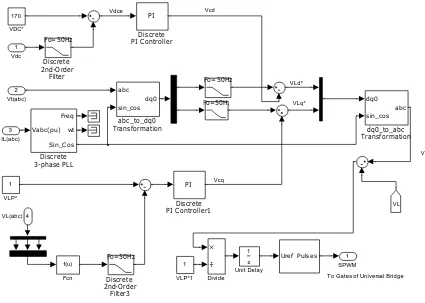
3.3 Synchronous Reference Frame Theory Based Control Algorithm
This theory is based on Parks Transformation. Here we transform the PCC voltage (Vt) in to d-q and then flow
goes as shown in figure: 2.After Controller actions the result is converted back to a-b-c frame these are the
reference signals which are compared with actual load Voltage(VL) at load bus. The difference signals are fed to
PWM generator. The PWM generator gives a sequence of six pulses to control the IGBT based convertor, the
universal bridge as shown in Figure :1.
v*Ld = v td_dc - vcd (9)
v*Lq = v tq_dc + vcq (10)
where v*Ld and v*Lqare estimatedDC componentsof active and reactive voltage component of reference
load voltages in d-q frame. vtq_dc and v td_dc corresponding to the source side active and reactive powers and
vcd and vcq are the discrete PI controller outputs corresponding to required active voltage component for
self-supporting DC bus and required reactive voltage component for voltage regulation at load terminal
respectively.
Ripple filter
Sensitive 3 Phase LOAD
5kva,(415V) 3 Phase Source
(415V,10KVA)
Unprotected 3 Phase LOAD
5kva,(415V) Za Zb Zc Lr Lr Lr Rr ,Cr Rr ,Cr Rr ,Cr Discrete, Ts = 5e-005 s.
powergui v
+
-A B C A B C
A1+ A1 B1+ B1 C1+ C1 A2+ A2 B2+ B2 C2+ C2
Series Injection Transformer
52 |
P a g e
Figure 2 Synchronous Reference Frame Theory (SRFT) Based Controller
f(u) is a function used to compute vLpas shown in fig 4.2 is given by equation 4.3
vLp =
2 (𝑉𝐿𝑎2+𝑉𝐿𝑏2+𝑉𝐿𝑐2)
3 (11)
Where vLpis the computed magnitude of the sensed load voltage in p.u. and V*Lpis the reference magnitude of
load voltage in p.u. .The d-q components of PCC voltages are computed as per the standard park
transformation .
IV. RESULTS AND DISCUSSION
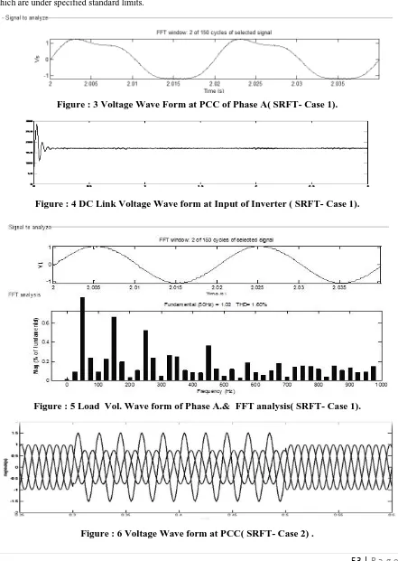
Case:1
Two types of Disturbances are superimposed on balanced three phase positive sequence source which effects
unbalance in all three phases. First disturbance adds harmonics of Order: 3, Amplitude: 0.2 p.u, Phase Shift:
-250 and Sequence: Zero. Second disturbance adds harmonics of Order: 2, Amplitude: -0.2 p.u, Phase Shift: 350
and Sequence: Negative. For the sake of clarity waveforms of phase A are only presented though waveform
distortion takes place in all three phases. In the same way DVR also smoothens all three phases but phase A is
only shown. DVR restores all three phases.
This controller works satisfactorily for Removal of Harmonics. The THD of Supply Voltage is 18.9%.It reduces
THD to 1.41%.(avg) and restores magnitude to 1.02 p.u.(avg) .
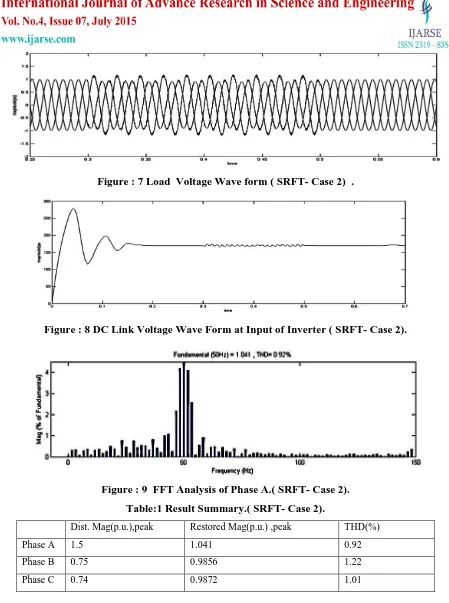
Case:2
Two types of Disturbances are superimposed on balanced three phase positive sequence source which effects
unbalance in all three phases. First disturbance is of Order: 1, Amplitude: 0.3 p.u, Phase Shift: -250 and
Vdce Vcd
Vcq
VLd*
VLq*
VL*
53 |
P a g e
Sequence: Zero. Second disturbance is of Order: 1, Amplitude: 0.2 p.u, Phase Shift: 350 and Sequence:
Negative. For the sake of clarity FFT analysis of phase A is only presented .
This controller works satisfactorily for Removal of unbalance. Using FFT analysis tool of MATLAB
SIMULINK we come to know that DVR restores magnitude about 1.004(avg. ) and THD to 1.05% (avg. )
which are under specified standard limits.
Figure : 3 Voltage Wave Form at PCC of Phase A( SRFT- Case 1).
Figure : 4 DC Link Voltage Wave form at Input of Inverter ( SRFT- Case 1).
Figure : 5 Load Vol. Wave form of Phase A.& FFT analysis( SRFT- Case 1).
54 |
P a g e
Figure : 7 Load Voltage Wave form ( SRFT- Case 2) .
Figure : 8 DC Link Voltage Wave Form at Input of Inverter ( SRFT- Case 2).
Figure : 9 FFT Analysis of Phase A.( SRFT- Case 2).
Table:1 Result Summary.( SRFT- Case 2).
Dist. Mag(p.u.),peak Restored Mag(p.u.) ,peak THD(%)
Phase A 1.5 1.041 0.92
Phase B 0.75 0.9856 1.22
Phase C 0.74 0.9872 1.01
V. CONCLUSION
Synchronous Reference based self supported DVR works satisfactorily for the two cases discussed the results
55 |
P a g e
5.1 Appendix
REFRENCES
[1] N.G.Hingorani and L.Gyuagi,‖Understanding Facts: concepts and Technology of Flexible AC
Transmission Systems‖,(Book)IEEE press, New York,2000.
[2] K.R.Padiyar ―FACTS Controllers in Power Transmission and Distribution ‖,(Book) New Age
International(P) limited , Publishers, New Delhi, 2007.
[3] Math H.J. Bollen, ―Understanding power quality problems :voltage sags and Interruptions‖ ,(Book)IEEE
press, New York, 2000.
[4] R.C. Dugan, M.F. McGranaghan and H.W.Beaty, Electric Power Systems Quality, 2ed Edition ,(Book)
McGraw Hill, Newyork, 2006.
[5] Stump, M.D., Keane, G.J., and Leong, F.K.S, ―The Role of Custom Power Products in Enhancing Power
Quality at Industrial Facilities‖, in Proc.IEEE Energy Management and Power Delivery ’98 Vol .2, pp.
507-5 17. March 1998.
[6] BOLLEN, M.H.J., ―Voltage Sags in Three Phase Systems‖. IEEE Power Engineering Review, vol.21 No.
9 ,pp. 8-15. Sept 2001.
[7] D. Daniel Sabin and AmbraSannino, ―A Summary of the Draft IEEE P1409 Custom Power Application
Guide‖, Transmission and Distribution Conference and Exposition, IEEE PES, vol. 3, pp. 931-936, 7-12
Sept 2003.
[8] C. Alvarez, J. Alamar, A. Domijan Jr., A. Montenegro, and Song, ―An investigation toward new
technologies and issues in power quality,‖ in Proc. 9th Int. Conf. Harmon. Qual. Power, vol. 2, pp. 444–
449, 2000.
[9] Masoud Aliakbar Golkar, ―Power Quality in Electric Networks: Monitoring and Standards‖ the second
world engineering conference, pp. 137-141 July 2002.
SYSTEM DATA OF SELF SUPPORTED DVR
System Element Ratings
AC Main Supply 3Phase, 440V , 50Hz, 10KVA.
DC Link Voltage 170V. Filter
Elements
Rr=3
, Lr= 3 mH& Cr=10µFInjection Transformer 170/250,10KVA
Load 3Phase RL balanced 5KW,440V. pf=0.9.
Universal Bridge IGBT based, PWM switching Frequency:6KHz
56 |
P a g e
[10] N.G. Hingorani, ―Introducing Custom Power", IEEE Spectrum, vol. 32, pp. 41-48, 1995.Force, 2003
[11] Yash Pal, A. Swarup and Bhim Singh, ―A Review of Compensating Type Custom Power Devices for
Power Quality Improvement‖ IEEE Power India Conference, New Delhi pp. 1-8, 12-15Oct 2008.
[12] Fawzi AL Jowder ―Modeling and Simulation of Different System Topologies for Dynamic Voltage
Restorer‖ IEEE International Conference on Electric Power and Energy Conversion Systems, EPECS '09.
Sharjah, pp. 1-6, Nov 2009.
[13] John Godsk Nielsen and FredeBlaabjerg ―Control Strategies for Dynamic Voltage Restorer Compensating
Voltage Sags with Phase Jump‖, Applied Power Electronics Conference and Exposition, IEEE, vol. 2, pp.
1267-1273, 2001.
[14] D.N.Katole ―Analysis and Mitigation of Balanced Voltage Sag with the Help of Energy Storage System‖ ,
3rd International Conference on Emerging Trends in Engineering and Technology ,Goa, India , pp.
317-321, Nov 2010.
[15] Arindam Ghoshand Gerard Ledwich, ―Compensation of Distribution System Voltage Using DVR‖ IEEE
Transactions on Power Delivery, vol. 17, No. 4, pp.1030-1036, Oct 2002.
[16] Chi-Jen Huang, Shyh-Jier Huang and Fu-Sheng Pai, ―Design of Dynamic Voltage Restorer With
Disturbance-Filtering Enhancement‖ IEEE Transactions on Power Electronics, vol. 18, No. 5,
pp.1202-1210, Sept 2003.
[17] D. MahindaVilathgamuwa, A. A. D. RanjithPerera, and S. S. Choi ―Voltage Sag Compensation With
Energy Optimized Dynamic Voltage Restorer ―IEEE Transactions on Power Delivery, Vol. 18, No. 3,
pp.928-936, July 2003.
[18] Arindam Ghosh , Amit Kumar Jindal, Avinash Joshi, ―Design of a Capacitor – Supported Dynamic
Voltage Restorers for Unbalanced and Distorted Loads‖ , IEEE Transactions on Power Delivery Vol.19
,No.1, pp. 405-413 , 2004.
[19] Fitzer C., Barnes, M. and Green P., ―Voltage Sag Detection Techniquefor a Dynamic Voltage Res torer‖.
IEEE Transactions on Industry Applications, vol.40,No.1, pp. 203-212, 2004.
[20] John Godsk Nielsen and FredeBlaabjerg, ―A Detailed Comparison of System Topologies for Dynamic
Voltage Restorers‖, IEEE Transactions on industry Applications, vol. 41, No. 5 pp.1272-1280, , Sept/Oct
2005.
[21] D. MahindaVilathgamuwa, H. M. Wijekoon, and S. S. Choi, ―A Novel Technique to Compensate Voltage
Sags in Multiline Distribution System—The Interline Dynamic Voltage Restorer‖ IEEE Transactions on
Industrial Electronics, vol.53, No.5,pp.1603-1611, Oct 2006.
[22] Yun Wei Li, D. MahindaVilathgamuwa,Poh Chiang Loh and FredeBlaabjerg, ―A Dual-Functional
Medium Voltage Level DVR to Limit Downstream Fault Currents‖ IEEE Transactions on Power
Electronics, vol. 22, No. 4, pp.1330-1340, July 2007.
[23] Carl Ngai-man Ho, Henry S. H. Chung, and Keith T. K. Au ‖ Design and Implementation of a Fast
Dynamic Control Scheme for Capacitor-Supported Dynamic Voltage Restorers‖ IEEE Transactions on
57 |
P a g e
[24] Christoph Meyer, Rik W. De Doncker, Yun Wei Li, andFredeBlaabjerg, ―Optimized Control Strategy for
a Medium-Voltage DVR—Theoretical Investigations and Experimental Results‖ IEEE Transactions on
Power Electronics, vol. 23, No. 6, pp.2746-2754. Nov 2008.
[25] Jing Shi, Yuejin Tang, Kai Yang, Lei Chen, Li Ren, Jingdong Li, and Shijie Cheng, “SMES Based
Dynamic Voltage Restorer for Voltage fluctuations Compensation‖ IEEE transactions on Applied
Superconductivity. vol. 20, No. 3, pp.1360-1364. June 2010.
[26] ParagKanjiya, Bhim Singh, Ambrish Chandra, and Kamal Al-Haddad, ―SRF Theory Revisited to Control
Self-Supported Dynamic Voltage Restorer (DVR) for Unbalanced and Nonlinear Loads‖ IEEE
Transactions on industry Applications, vol. 49, No. 5, pp.2330-2340, Sept/Oct 2013.
[27] ParagKanjiya, ―Modeling ,Design,Control and Implementation of Dynamic voltage Restorer (DVR)‖
,M.tech. dissertation, IIT, EE Dept., Delhi, 2011.
AUTHORS
1.Indu bhushan received the B.Tech (Electrical Engg.) and M.Tech ( Instrumentation & control System )
Degree Degree from Chhotu Ram State College Of Engg. Sonipat, MDU , Rohtak, Harayana , India. Her
research interests are Power System, Electrical Machines, High Voltage Engg.
2.Abhay kr.Shah received the B.Tech (Electrical & Electronics Engg.) Degree from Gautam Budh Technical
University Formely UPTU, Lucknow, India.He received M.Tech ( Power System ) Degree in the Department of
Electrical & Electronics Engineering, AFSET, MDU Rohtak, Haryana India . His research interests are Power