THE ELECTROSTATIC POTENTIAL ASSOCIATED TO INTERFACE PHONON MODES IN NITRIDE SINGLE HETEROSTRUCTURES
M. E. Mora-Ramos and R. P´erez-Alvarez
Facultad de Ciencias
Universidad Aut´onoma del Estado de Morelos Mexico
V. R. Velasco
Instituto de Ciencia de Materiales de Madrid CSIC
Spain
Abstract—The electrostatic potential associated to the interface oscillation modes in nitride-based heterostructure is calculated with the use of a complete phenomenological electroelastic continuum approach for the long wave optical oscillations, and the Surface Green Function Matching technique. The crystalline symmetries of zincblende and — isotropically averaged — wurtzite are both considered in the sets of input bulk frequencies and dielectric constants.
1. INTRODUCTION
interaction Hamiltonian presented in [1]. The outcome of their calculation revealed values for the room temperature mobility well below the most of the experimental reports in such kind of systems. Since several different approaches for the calculation of single electron conduction band states were tested, the problem seems to be related with the particular approach for the optical phonon modes that arises from the uniaxial DCM.
The discussion about the suitability of the DCM for a complete phenomenological description of the optical phonon in polar semiconducting heterostructures dates back to the early nineties [6, 7]. The limitation of the DCM for dealing with the mechanical boundary conditions was then highlighted, and a continuum phenomenological electroelastic model (CPELM) was proposed instead. This model was later applied to the study of polar optical phonon modes in AlGaAs/GaAs single heterostructures [8], in combination with the method of Surface Green Function Matching (SGFM).
2. SOME COMMENTS ON THE THEORY
We will use the CPELM-SGFM formalism in the present article. Due to its rather involved mathematical framework, the reader is referred to references [6–9] for details.
The CPELM deals exclusively with systems made of semiconduc-tors with cubic crystalline symmetry. Nevertheless, we believe that some new information, regarding the interface phonon modes, can be derived with its application to heterostructures of materials bearing hexagonal symmetry such as the wurtzite nitrides. For this purpose, the procedure implies the isotropic averaging of the main input pa-rameters of the model. These are the bulk longitudinal and transver-sal phonon frequencies at the Brillouin Zone center, and the dielectric constants. Besides, it is also needed to average the values of the param-etersβL, andβT. They are related to the phonon dispersion curves in
the bulk, which can be well approximated byω2L(q) =ωLO2 −βL2q2, and by ωT2(q) =ωT O2 −βT2q2, for the longitudinal and transversal phonons respectively. Since the CPELM is a long wavelength model, its appli-cation is usually restricted to a small region — of about 10% — of the Brillouin zone, around the Γ point. This is precisely the region where the parabolic approximation of the dispersion relation appropriately applies.
The work is restricted to deal with GaN-AlGaN structures. We are considering a system that consists of two half-space layers. The one made of AlxGa1−xN is located at the z < 0 region, while for
the following input parameters: ∞(GaN) = 5.30, ∞(AlN) = 4.46;
ρ(GaN) = 6.10 g/cm3, ρ(AlN) = 3.29 g/cm3 ωLO(GaN) = 748 cm−1,
ωLO(AlN) = 920 cm−1; ωT O(GaN) = 562 cm−1, ωT O(AlN) =
670 cm−1; βL2(GaN) = 1.52 × 10⁻¹¹, βL2(AlN) = 1.44 × 10⁻¹¹;
βT2(GaN) = 2.87×10⁻¹³,β2T(AlN) = 5.89×10⁻¹². The corresponding expressions for the cubic alloy AlxGa1−xN are obtained by applying the
Vegard’s law to each of them. That is, f(AlxGa1−x)N) = f(GaN)∗
(1−x) +f(AlN)∗x.
In the case of the wurtzite nitrides, we have: ∞(GaN) = 5.29,
∞(AlN) = 4.68; ρ(GaN) = 6.15 g/cm3, ρ(AlN) = 3.23 g/cm3, with
their corresponding Vegard’s laws. On the other hand, the parabolic dispersion amplitudes are: β2
zL(GaN) = 2.78 ×10⁻¹², βzL2 (AlN) =
2.47×10⁻¹¹; β⊥2L(GaN) = 7.60×10⁻¹², β⊥2L(AlN) = 2.28×10⁻¹¹;
βzT2 (GaN) = −2.53×10⁻¹²,βzT2 (AlN) = 7.34×10⁻¹²;β2⊥T(GaN) = −1.21×10⁻¹²,β⊥2T(AlN) = 2.69×10⁻¹²; Vegard’s law is also applied to these quantities, in order to deal with their values for the alloy.
The indexes “z” and “⊥” label theA1 andE1 infrared-active polar optical mode of the wurzite structure, respectively. The dependencies of the frequencies of these optical modes upon the aluminum molar fraction have been studied in greater detail. The longitudinal modes have a one-mode character. The corresponding frequencies are: ωzL =
734 + 153x+ 75x(1−x) cm−1,ω
⊥L= 7442 + 170x+ 65x(1−x) cm−1.
The transversal modes have two-mode character, GaN-like and AlN-like, with frequencies given by: ωz(GaN) = 532+65x−2x(1−x) cm−1,
ωz(AlN) = 551 + 55x; ω⊥(GaN) = 557 + 53xcm−1, ω⊥(AlN) =
617+47xcm−1. All these data have been collected from different works (see references [10–16]). To grant the application of the CPELM to the wurtzite heterostructures, the “z” and “⊥” values are isotropically averaged.
3. RESULTS AND CONCLUSIONS
Figures 1 and 2 show the local density of states (LDOS) for SHS with cubic and hexagonal symmetry, respectively. The peaks correspond to the value of the interface polar optical phonon oscillations. The set of LDOS peaks for different values of the phonon wavevectorκ generates the dispersion relation of the interface mode. These dispersion relations for nitride SHS are shown in Figure 3 for some values of the Al molar fractionx.
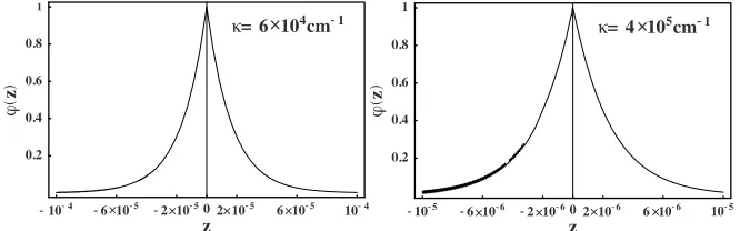
Figures 4 and 5 present the electrostatic potential correspond-ing to the GaN-like interface mode in wurtzite and zincblende AlxGa1−xN/GaN SHS respectively. The values of the phonon
oscilla-660 680 700 720 740 760 780 800 cm- 1
200 400 600 800 1000 1200 LDOS arb . units
κ= 8 104cm- 1
720 740740 760760 780 800 cm- 1
500 1000 1500 2000 LDOS arb . units
κ= 6 105cm- 1
( ) ( )
() ()
ω ω
× ×
Figure 1. LDOS in a zincblende Al0.22Ga0.78N/GaN SHS for phonon
wavevector κ = 8 × 104cm−1 SHS (left), and for a zincblende
Al0.33Ga0.67N/GaN SHS for wavevectorκ= 6×105cm−1 SHS (right).
700 720 740 760 780 800
cm-1 0 1000 3000 5000 7000 LDOS arb . units
= 2 105cm- 1
750 760 770 780 790 800 0 1000 2000 3000 4000 5000 LDOS arb . units
= 4 104 cm- 1
κ κ ( ) () ω ω × () ×
Figure 2. LDOS in a wurtzite Al0.22Ga0.78N/GaN SHS for phonon
wavevector κ = 2 × 105cm−1 SHS (left), and for a wurtzite Al0.40Ga0.60N/GaN SHS for wavevectorκ= 4×104cm−1 SHS (right).
0 2 106 4 106 6 106 8 106 κ 765 770 775 780 785 ωκ
x=0.4
x=0.33
x=0.22
0 106 2 106 3 106 4 106 5 106 6 106
κ 600 650 700 750 800 ωκ
x=0.4
x=0.22
() ()
× × × × × × × × ×
Figure 3. Dispersion relations for the interface polar optical oscillation mode in zincblende AlxGa1−xN/GaN SHS (left), and
-6 10-6-4 10-6-2 10-6 0 2 10-64 10-66 10-6
z
0.2 0.4 0.6 0.8 1
ϕ
z
κ=106cm-1
-6 10-5-4 10-5-2 10-5 0 2 10-5 4 10-5 6 10-5
z
0.2 0.4 0.6 0.8 1
ϕ
z
κ=105cm-1
() ()
× × × × × × × × × × × ×
Figure 4. Electrostatic potential function corresponding to the GaN-like interface phonon mode in wurtzite AlxGa1−xN/GaN SHS. In this
case: x = 0.22, κ = 106cm−1 (left), and x = 0.33, κ = 105cm−1 (right). Arbitrary units are used on both axes.
-10-4 -6 10-5 -2 10-50 2 10-5 6 10-5 10-4
z
0.2 0.4 0.6 0.8
1
ϕ
z
κ=6 104cm-1
-10-5 -6 10-6 -2 10-60 2 10-6 6 10-6 10-5
z
0.2 0.4 0.6 0.8 1
ϕ
z
κ=4 105cm-1
() ()
× × × × × × × ×
× ×
Figure 5. Electrostatic potential function corresponding to the GaN-like interface phonon mode in zincblende AlxGa1−xN/GaN SHS. In this
case: x= 0.33,κ= 6×104cm−1(left), andx= 0.40,κ= 4×105cm−1
(right). Arbitrary units are used on both axes.
tory behavior is observed on the AlGaN side of the SHS. In fact, the amplitude of the small oscillations ofφ in that region depends on the magnitude of the phonon wavevector. It is more apparent for higher values ofκ. To explain this, one should remember that we are studying the GaN-like modes only. For these modes it fulfills thatω(κ)< ωLO
in the regionz <0.
ACKNOWLEDGMENT
M. E. M. R. acknowledges support from CONACyT through Grant 52304.
REFERENCES
1. Lee, B. C., K. W. Kim, M. A. Stroscio, and M. Dutta, “Optical-phonon confinement and scattering in wurtzite heterostructures,” Phys. Rev. B, Vol. 58, No. 8, 4860–4865, 1998.
2. Shi, J.-J, “Interface optical phonon modes and electron-interface-phonon interactions in wurtzite GaN/AlN quantum wells,”Phys. Rev. B, Vol. 68, No. 16, 165335(1)–165335(11), 2003.
3. Shi, J.-J, X. L. Chu, and E. M. Goldys, “Propagating optical-phonon modes and their electron-optical-phonon interactions in wurtzite GaN/AlxGa1−xN quantum wells,” Phys. Rev. B, Vol. 70, No. 11,
115318(1)–115318(8), 2004.
4. Li, L., D. Liu, and J. J. Shi, “Electron-quasi-confined-optical-phonon interactions in wurtzite GaN/AlN quantum wells,” Eur. Phys. J. B, Vol. 44, No. 4, 401–413, 2005.
5. Mora-Ramos, M. E., J. Tutor, and V. R. Velasco, “Interface-phonon-limited two-dimensional mobility in AlGaN/GaN het-erostructures,” J. Appl. Phys., Vol. 100, No. 12, 123708(1)– 123708(9), 2006.
6. Trallero-Giner, C., F. Garc´ıa-Moliner, V. R. Velasco, and M. Cardona, “Analysis of the phenomenological models for long wavelength polar optical modes in semiconductor layered systems,”Phys. Rev. B, Vol. 45, No. 20, 11944–11948, 1992. 7. Garc´ıa-Moliner, F., “Long wave polar optical phonons in
heterostructures,” Phonons in Semiconductor Nanostructures: Proceedings of the NATOAdvanced Research Workshop, J.-P. Leburton, J. Pascual, and C. Sotomayor-Torres (eds.), Kluwer Academic Publishers 1993, 1–12, St. Feliu De Guixols, Spain, September 1992.
8. Chubykalo, A., V. R. Velasco, and F. Garc´ıa-Moliner, “Polar optical phonons at semiconductor interfaces,”Surf. Sci., Vol. 319, Nos. 1–2, 184–192, 1994.
9. Mora-Ramos, M. E. and D. A. Contreras-Solorio, “The polaron in a GaAs/AlAs quantum well,” Physica B, Vol. 253, No. 3-4, 325–334, 1998.
A. P. Mirgorodsky, and R. A. Evarestov, “Phonon dispersion and Raman scattering in hexagonal GaN and AlN,” Phys. Rev. B, Vol. 58, No. 19, 12899–12907, 1998.
11. Zi, J., X. Wan, G. Wei, K. Zhang, and X. Xie, “Lattice dynamics of zinc-blende GaN and AIN: l. Bulk phonons,” J. Phys.: Cond. Matt., Vol. 8, 6323–6328, 1996.
12. Bechstedt, F. and H. Grille, “Lattice dynamics of ternary alloys,” Phys. Stat. Sol. (B), Vol. 216, 761–768, 1999.
13. Bechstedt, F., J. Furthm¨uller, and J.-M. Wagner, “Electronic and vibrational properties of group-III nitrides: Ab initio studies,” Phys. Stat. Sol. (C), Vol. 0, 1732–1749, 2003.
14. Santos, A. M., E. C. F. Silva, O. C. Noriega, H. W. L. Alves, J. L. A. Alves, and J. R. Leite, “Vibrational properties of cubic AlxGa1−xN and InxGa1−xN ternary alloys,”Phys. Stat. Sol. (B),
Vol. 232, 182–187, 2002.
15. Bougrov, V., M. E. Levinshtein, S. L. Rumyantsev, and A. Zubrikov, “GaN, AlN, InN, BN, SiC, SiGe,” Poperties of Advanced Semiconductor Materials, M. E. Levinshtein, S. L. Rumiantsev, and M. S Shur (eds.), John Wiley, New York, 2001.