ISSN (Print) : 2320 – 3765 ISSN (Online): 2278 – 8875
I
nternational
J
ournal of
A
dvanced
R
esearch in
E
lectrical,
E
lectronics and
I
nstrumentation
E
ngineering
(An ISO 3297: 2007 Certified Organization)
Vol. 5, Issue 2, February 2016
Flexible Output Voltage and Improved
Conversion Efficiency Using Three-Level
Quasi-Two-Stage Single-Phase PFC Converter
S.Divyapriya 1, R.Arun Kumar 2
M.E Student (Power Electronics and Drives), Dept. of EEE, Mount Zion College of Engineering and Technology,
Pudukkottai, Tamil Nadu, India.
Assistant Professor, Dept. of EEE, Mount Zion College of Engineering and Technology, Pudukkottai, Tamil Nadu,
India.
ABSTRACT: This framework exhibits a three-level semi two-stage single-stage Power Factor Correction [PFC] converter that has adaptable yield voltage and enhanced change proficiency. The proposed PFC converter elements sinusoidal data present, three-level yield trademark, and an extensive variety of yield DC voltages, and it will be exceptionally suitable for high power applications where the yield voltage can be either lower or higher than the top AC information voltage, for instance Plug-in Hybrid Electric Vehicle (PHEV) charging frameworks. Also, the included DC/DC buck transformation stage might just need to process halfway info control as opposed to full size of the data power, and hence the framework general proficiency can be quite moved forward. Through appropriate control of the buck converter, it is additionally conceivable to moderate the twofold line recurrence swell power that is innate in a solitary stage AC/DC framework, and the subsequent burden end voltage will be genuinely steady. The dynamic reaction of this regulation circle is additionally quick and the framework is along these lines uncaring to outer unsettling influences. Both reenactment and test results are introduced to demonstrate the viability of this converter and in addition its proficiency change against a traditional two-stage arrangement.
KEYWORDS: AC-to-DC, Converter Unit, Decoupling, Regulator Unit, Electric Vehicle Charger, PFC-Power Factor Correction
I. INTRODUCTION
ISSN (Print) : 2320 – 3765 ISSN (Online): 2278 – 8875
I
nternational
J
ournal of
A
dvanced
R
esearch in
E
lectrical,
E
lectronics and
I
nstrumentation
E
ngineering
(An ISO 3297: 2007 Certified Organization)
Vol. 5, Issue 2, February 2016
A typical issue for these topologies is that there is no immediate vitality exchange way amid force transformation and all data power must be prepared by dynamic switches and put away by middle of the road detached parts (either inductors or capacitors) before being supplied to the end loads. This shows the segments will be working under expanded voltage/current anxieties, which might hence prompt diminished force thickness and change effectiveness. Keeping in mind the end goal to enhance the execution of Cuk and SEPIC based PFC topologies, their bridgeless variations have as of late been proposed in with the vast majority of them being worked in broken conduction mode (DCM). For this situation, the PFC c nverter can be built with less semiconductor switches and the on-state conduction misfortunes can be lessened. The exchanging misfortunes are lessened too because of their DCM operation. In any case, the fundamental force switches in these bridgeless topologies are still under high voltage stress and the DCM operation additionally suggests that they are suitable for generally low power applications in light of the high top current in the support inductor. In perspective of this, AC/DC converters with direct buck ability are profoundly coveted in high power PHEV battery charger applications and a buck sort PFC topology, named as Swiss Rectifier has as of now been proposed for three-stage AC/DC frameworks. For single-stage AC/DC rectifiers, a great deal research works have been as of late completed to ponder the execution and operation of a buck topology based PFC converter, which can deliver a lower yield DC voltage and in the interim keep up high proficiency under all inclusive line voltage.
The bridgeless subsidiary of the buck PFC was additionally proposed to assist enhance its transformation proficiency. Lamentably, such buck PFC converters might characteristically subject to a socalled "dead point" restriction when the info voltage is lower than the yield voltage. The AC side information current can't be controlled to be absolutely sinusoidal and solidarity power component is not achievable. An enhanced buck PFC converter with high power element is proposed, where a helper switch and two diodes are included the circuit to give current regulation amid the "dead edge" period. Despite the fact that the force variable can be enhanced, the data current waveform is still not sinusoidal and subsequently, they might just be suited for low power applications (under 1kW), e.g. tablet connector, TV sets power supplies. Another buck PFC converter with force decoupling capacity has as of late been proposed, and it includes superb data present and additionally swell free yield voltage. Be that as it may, the confinement of this topology is that, its yield voltage must be lower than half of the crest AC information voltage, and this might to a great extent oblige the yield voltage range amid low line operation.
Some incorporated bidirectional AC/DC and DC/DC converter topologies were proposed, which joins all essential operation modes that are required for the force converter of PHEVs, specifically module charging from force network, vehicle-to-grid (V2G) release, pumping energy to drive electric engine, and regenerative braking. Regardless of its intense functionalities, these converters include various semiconductor gadgets, and in this way it may not be a productivity upgraded and practical arrangement. To give a basic however viable arrangement, this paper displays a high productivity single-stage PFC converter that elements sinusoidal info present, three-level yield trademark and adaptable yield DC voltage. Its engaging quality is that, in the event of buck operation mode, the inserted bidirectional DC/DC converter might just need to process fractional data control instead of full size of the information power, and thusly its transformation effectiveness can be greatly enhanced as contrasted and the ordinary two-stage arrangement. Additionally, the PFC stage displays three-level yield voltage, and the dV/dt over the switches are diminished, so as the exchanging misfortunes. An additional advantage of this converter is that, the fluctuating 100/120Hz symphonious force in the single-stage framework can be verging on redirected into the dc-join capacitor through appropriate control plan, and the heap voltage will be genuinely steady and of quick element reaction. The operation standard and control systems of the proposed three-level PFC converter are examined in points of interest in this paper, and both reproduction and trial results are given to acceptance of its viability.
A. Operating Principles and System Analysis
ISSN (Print) : 2320 – 3765 ISSN (Online): 2278 – 8875
I
nternational
J
ournal of
A
dvanced
R
esearch in
E
lectrical,
E
lectronics and
I
nstrumentation
E
ngineering
(An ISO 3297: 2007 Certified Organization)
Vol. 5, Issue 2, February 2016
rectifier bridge should be replaced by an unfolding bridge, and D1 and D2 should be replaced by IGBTs with anti-parallel diodes.
Figure-1. Circuit diagram of the proposed three-level PFC converter for single-phase PHEV chargers
As mentioned above, the proposed three-level PFC has a wide range of output voltages and it can function as either a buck or a boost converter. During buck operation, there are two operation modes for Q1 and Q2. When the low DC bus
voltage or simply the load voltage VL is higher than the instantaneous input voltage Vin|sinωt|, where Vin is the peak value of input voltage and ω is the fundamental angular frequency, Q2 will be always on. Q1 and D1 then form up a
standard boost PFC that directly converts input power for DC load consumption, and the converter pole voltage VAB will be changed between 0 and VL. It should be noted that, in this operation period, Q3 and Q4 of the buck converter theoretically do not need to switch because all input power can be directly supplied into the load through D1 and Q2. However, in order to obtain a smooth output voltage, Q3 and Q4 still need to work and provide ripple power compensation during this operation period.
ISSN (Print) : 2320 – 3765 ISSN (Online): 2278 – 8875
I
nternational
J
ournal of
A
dvanced
R
esearch in
E
lectrical,
E
lectronics and
I
nstrumentation
E
ngineering
(An ISO 3297: 2007 Certified Organization)
Vol. 5, Issue 2, February 2016
In the second operation interval when VL is less than Vin|sinωt|, Q1 remains off. Q2 and D2 will modulate
and form up another boost PFC. In this case, the converter pole voltage VAB is changing between VL and the high DC bus voltage VH. It should be noted that, in this operation period, Q3 and Q4 of the buck converter theoretically do not need to switch because all input power can be directly supplied into the load through D1 and Q2. However, in order to obtain a smooth output voltage, Q3 and Q4 still need to work and provide ripple power compensation during this
operation period. In the second operation interval when VL is less than Vin|sinωt|, Q1 remains off. Q2 and D2 will
modulate and form up another boost PFC.
In this case, the converter pole voltage VAB is changing between VL and the high DC bus voltage VH. Intuitively, when D2 is conducting, excessive input power will be flowing into the dc-link capacitor CH and this high bus voltage will be subsequently stepped down by the bidirectional DC/DC converter to cater for load consumption, and this is the root reason that why the DC/DC converter may only process partial input power and higher conversion efficiency can be obtained through the proposed topology. The idealized operating waveforms during these two modes are presented in Fig. 2. In order to ensure smooth transition between the low and high voltage level commutations, an offset is injected into the carrier of the pulse-width modulation (PWM) for Q2 as shown in Fig. 2.
B. System Controller Design
The control system of the proposed three-level AC/DC converter will be relatively more complicated than that of a conventional boost PFC, because it requires at least two voltage control loops to regulate the output voltage VL and the dc-link voltage VH, respectively. Also, the intermittent operation of Q1 and Q2 imposes a disturbance to the system, and a fast control loop must be designed to reject this periodic disturbance. In order to realize these control objectives, two independent control loops are designed for controlling the PFC stage and the buck stage, respectively, and the control algorithms will be elaborated as follows.
A. PFC Converter Control
A classic cascaded control structure is employed to regulate the PFC converter. Its outer voltage control loop is tasked at balancing input and output power, and the dc-link voltage VH is chosen as the control variable because the charging power into the dc-link capacitor CH is directly proportional to input power as long as VL, Vin, and VH are fixed. This voltage control loop will also maintain the average value of VH to be constant, whereas its instantaneous value is not necessary to be constant, because the dc-link capacitor CH has to absorb the double line frequency harmonic in this single-phase system. The control loop is therefore of slow response and its control bandwidth is set below 20Hz as per usual design, and this is realized by tuning the parameters of a proportional-integral (PI) regulator Gv(s) as follow,
Gv(S) = Kpv(1+(1/TvS))
where Kpv is the proportional gain to adjust control bandwidth, and τv is the time constant of the integral term to
achieve high DC compensation gain. In order to prevent the dc-link ripple voltage from distorting the reference of inner
current control loop, a second order notch filter tuned at 2ω is added at the output of the PI regulator.
G nothch (S) = (s2 + (2w)2)/(s2 + K2S + (2w)2)
In addition to the buck operation, the proposed PFC can also function as a boost and this operation mode is triggered when Vin<VL<VH. In this case, the modulation scheme discussed above is still applicable. According to (2), the duty cycle of Q2 will be greater than 1, implying that Q2 is always on. Therefore, the proposed circuit is simplified as a conventional two-level PFC that is comprised of Q1 and D1 only, and the buck converter is only used for ripple power compensation.
B. Buck Converter Control
ISSN (Print) : 2320 – 3765 ISSN (Online): 2278 – 8875
I
nternational
J
ournal of
A
dvanced
R
esearch in
E
lectrical,
E
lectronics and
I
nstrumentation
E
ngineering
(An ISO 3297: 2007 Certified Organization)
Vol. 5, Issue 2, February 2016
Figure 3. Instantaneous power distribution in the PFC converter and the buck converter, given fixed gird voltage, output voltage, and dc-link voltage
Therefore, a single voltage control loop is designed for this power stage to expedite its dynamic response and also to save a current transducer. Another reason for pursuing fast response of this voltage control loop is that it has to reject the periodic disturbance induced by its intermittent operation. Again, using the small signal modelling approach and assuming that the equivalent load resistance Rload is much larger than the ESRs and the filter inductance Ldc, the control duty cycle-to-output voltage transfer function Gvd_dc(s) of the bidirectional buck converter can be derived as,
where ωo is the LC resonant frequency introduced by the output filter. RCL is the ESR of the output capacitor CL and it introduces a zero ωz in the open loop gain. RLdc is the ESR of the boost inductor and these two ESRs together determine the quality factor Q of this second order system and they can provide damping effect to the LC resonance. Using the parameters listed in Table I, the Bode diagram of (12) can then be plotted as dotted line in Fig. 5. As shown, its closed-loop control system is inherently stable even a simple proportional gain is used. However, if the crossover frequency of this control loop is tuned to be less than one tenth of the switching frequency, e.g. 1kHz, the system phase margin is only 17°, which is obviously insufficient and may cause transient oscillations. Furthermore, this system has limited DC gain, and its steady-state tracking error may not be zero.
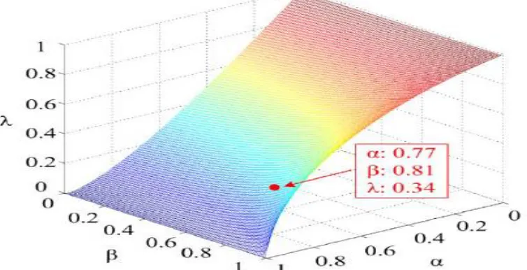
Figure 4. 3D plot of (7) showing the percentage of input power converted by the buck converter as a function of
ISSN (Print) : 2320 – 3765 ISSN (Online): 2278 – 8875
I
nternational
J
ournal of
A
dvanced
R
esearch in
E
lectrical,
E
lectronics and
I
nstrumentation
E
ngineering
(An ISO 3297: 2007 Certified Organization)
Vol. 5, Issue 2, February 2016
The Bode diagrams for the designed type III compensator and the compensated system open loop gain are presented in Fig. 6 as dashed line and solid line, respectively, and it is demonstrated that 63.8° phase margin is successfully achieved when the system crossover frequency is placed at 974Hz, and this confirms its stable operation and fast transient response.
Figure 5. Overall control block diagram for the proposed three-level PFC converter
C. Discussion on Alternative Control Strategies
Since the charging power into the output capacitor CL is also proportional to the PFC’s input power, an alternative control strategy is to use VL, instead of VH, as the control variable for voltage regulation of the PFC converter. The bidirectional DC/DC converter will then be controlled by VH and it essentially becomes a DC/DC boost converter. As discussed, this dc-link voltage control loop should be of fast response in order to compensate system harmonics and disturbance, which means that its reference voltage is no long constant. Instead, its reference voltage must contain double line frequency component in order to absorb those AC side harmonics, and this reference cannot be obtained readily. Furthermore, it is well known that the boost converter has a right-half plane (RHP) zero and it will be more difficult to stabilize than a buck converter. This is especially true when a single voltage control loop is implemented and fast dynamic response is required in the system. Therefore, this control scheme is not chosen for the case studied here.
ISSN (Print) : 2320 – 3765 ISSN (Online): 2278 – 8875
I
nternational
J
ournal of
A
dvanced
R
esearch in
E
lectrical,
E
lectronics and
I
nstrumentation
E
ngineering
(An ISO 3297: 2007 Certified Organization)
Vol. 5, Issue 2, February 2016
In fact, other control strategies, like feed-forward of input voltage, implementing another inner current control loop, and adding nonlinear control element, can also be employed to further enhance the performance of the buck converter. However, they require even more sophisticated design efforts and are not compulsory for this application. The type III compensator discussed above will suffice for regulation of the proposed converter from both steady-state and transient points of view.
D. Simulation and Experimental Results
Simulation study was carried out in Matlab/Simulink environment and the circuit parameters are listed in Table I. The steady-state operation waveforms are presented in Fig. 7. It can be seen that Q1 and Q2 operate alternatively and may produce the desired three-level converter pole voltage VAB. The high level bus voltage is not constant because the dc-link capacitor needs to absorb the system double line frequency harmonic. This fluctuation voltage has basically no impact to the regulation of the boost inductor current, because it can be easily compensated by the fast current control loop. Thanks to the feed-forward mechanism of the open loop duty cycle, the grid current is almost sinusoidal and in phase with the grid voltage, and its ripple component is very small because of the three-level output voltage. As mentioned before, the buck converter theoretically does not need to switch when D2 is blocking. However, in order to deal with the system harmonic power and ensure constant load voltage, the buck converter still has to work during this operation mode. A 2kW prototype circuit was built in the laboratory for experimental validation of the proposed PFC converter and the circuit parameters are basically the same as those used in simulation, despite some very slight differences due to the tolerance of passive components.
II. RELATED WORK
In "Performance evaluation of bridgeless PFC boost rectifiers", the authors L. Huber, Y. Jang, and M. M. Jovanovic, quoted on, in this approach, a systematic review of bridgeless power factor correction (PFC) boost rectifiers, also called dual boost PFC rectifiers, is presented. Performance comparison between the conventional PFC boost rectifier and a representative member of the bridgeless PFC boost rectifier family is performed. Loss analysis and experimental efficiency evaluation for both CCM and DCM/CCM boundary operations are provided.
In "Evaluation and efficiency comparison of front end AC-DC plug-in hybrid charger topologies", the authors "Fariborz Musavi ; Res. Dept., Delta-Q Technol. Corp", quoted on, As a key component of a plug-in hybrid electric vehicle (PHEV) charger system, the front-end ac-dc converter must achieve high efficiency and power density. This paper presents a topology survey evaluating topologies for use in front end ac-dc converters for PHEV battery chargers. The topology survey is focused on several boost power factor corrected converters, which offer high efficiency, high power factor, high density, and low cost. Experimental results are presented and interpreted for five prototype converters, converting universal ac input voltage to 400 V dc. The results demonstrate that the phase shifted semi-bridgeless PFC boost converter is ideally suited for automotive level I residential charging applications in North America, where the typical supply is limited to 120 V and 1.44 kVA or 1.92 kVA. For automotive level II residential charging applications in North America and Europe the bridgeless interleaved PFC boost converter is an ideal topology candidate for typical supplies of 240 V, with power levels of 3.3 kW, 5 kW, and 6.6 kW.
ISSN (Print) : 2320 – 3765 ISSN (Online): 2278 – 8875
I
nternational
J
ournal of
A
dvanced
R
esearch in
E
lectrical,
E
lectronics and
I
nstrumentation
E
ngineering
(An ISO 3297: 2007 Certified Organization)
Vol. 5, Issue 2, February 2016
In "Ultraflat interleaved triangular current mode (TCM) single-phase PFC rectifier", the authors "Majid Pahlevaninezhad", quoted on, this approach presents a novel, yet simple zero-voltage switching (ZVS) interleaved boost power factor correction (PFC) ac/dc converter used to charge the traction battery of an electric vehicle from the utility mains. The proposed opology consists of a passive auxiliary circuit, placed between two phases of the interleaved front-end boost PFC converter, which provides enough current to charge and discharge the MOSFETs' output capacitors during turn-ON times. Therefore, the MOSFETs are turned ON at zero voltage. The proposed converter maintains ZVS for the universal input voltage (85 to 265 Vrms), which includes a very wide range of duty ratios (0.07-1). In addition, the control system optimizes the amount of reactive current required to guarantee ZVS during the line cycle for different load conditions. This optimization is crucial in this application since the converter may work at very light loads for a long period of time. Experimental results from a 3 kW ac/dc converter are presented in the paper to evaluate the performance of the proposed converter. The results show a considerable increase in efficiency and superior performance of the proposed converter compared to the conventional hard-switched interleaved boost PFC converter.
In "Ultra-fast dc-charge infrastructures for EV-mobility and future smart grids", the authors, "D. Aggeler", quoted on, now-a-days Power Electronics (PE) is entering more and more in technology which traditionally belongs to different engineering disciplines. E-mobility is one of these. Power Electronics in fact imposes itself as an emerging technology to enhance sustainable mobility, addressing all the engineering aspects starting from energy distribution for charging purposes until energy transformation on board of the traction related vehicles. This paper in particular focuses on newly developed PE infrastructure technologies enabling fast battery charging processes. Depending on the battery and vehicle type, a recharge sufficient for a travel range of more than 100km in less than 10 min is readily achievable. As battery technologies continuously advance, recharging will become available with the speed and simplicity of a today's fuel stop. Two PE converter architectures for recharging infrastructure applications will be presented and discussed based on both low-frequency (LF) and high-frequency (HF) isolation requirements. Technical evaluation of the two different technologies will be addressed and presented, including a pro- and contra analysis. The impact on the grid is studied by means of simulation with the assumption of a dc fast charging station placed in a rural area in Sweden.
In "A single-stage high-power-factor electronic ballast with ZVS buck–boost conversion", the authors "Hung L. Cheng", quoted on, this system proposes a novel single-stage high-power-factor electronic ballast via the integration of a derivative buck-boost converter and a half-bridge resonant inverter. The derivative buck-boost converter employs two coupled inductors with an appropriate turns-ratio to conduct the current from the input line source into the designated power switches. With the tactful topology and delicately designed circuit parameters, both the active power switches of the resonant inverter can retain the zero voltage switching (ZVS), resulting in a high circuit efficiency. A prototype circuit designed for a T8-36W rapid-start fluorescent lamp was built and tested to verify the analytical predictions, and satisfactory results were obtained experimentally.
III.BLOCK DIAGRAM
ISSN (Print) : 2320 – 3765 ISSN (Online): 2278 – 8875
I
nternational
J
ournal of
A
dvanced
R
esearch in
E
lectrical,
E
lectronics and
I
nstrumentation
E
ngineering
(An ISO 3297: 2007 Certified Organization)
Vol. 5, Issue 2, February 2016
IV.CIRCUIT DIAGRAM
Fig.3. Circuit Diagram
V. EXPERIMENTAL RESULTS
ISSN (Print) : 2320 – 3765 ISSN (Online): 2278 – 8875
I
nternational
J
ournal of
A
dvanced
R
esearch in
E
lectrical,
E
lectronics and
I
nstrumentation
E
ngineering
(An ISO 3297: 2007 Certified Organization)
Vol. 5, Issue 2, February 2016
Fig.5. Low Voltage Waveform
ISSN (Print) : 2320 – 3765 ISSN (Online): 2278 – 8875
I
nternational
J
ournal of
A
dvanced
R
esearch in
E
lectrical,
E
lectronics and
I
nstrumentation
E
ngineering
(An ISO 3297: 2007 Certified Organization)
Vol. 5, Issue 2, February 2016
Fig.7. Power Factor
VI.CONCLUSION
In this system, a three-level quasi-two-stage single-phase PFC converter has been presented. It has flexible output voltage and can be used for single-phase PHEV charger applications, where the battery voltage can be either lower or higher than the peak AC input voltage. The proposed converter features high quality input current, three-level output voltage, and improved conversion efficiency. By designing a fast regulation loop for the buck converter, the inherent fluctuating power issue in single phase systems can also be resolved, and the load voltage will be fairly constant and insensitive to load changes and external disturbances. Moreover, a dynamic gain compensator is implemented in the current control loop and in this case, its control bandwidth can be kept relatively constant irrespective of the DC bus voltage change during two different operation modes. Therefore, the grid current can be well regulated with low THD and high power factor. Experimental results obtained from a 2kW laboratory prototype have been presented in the paper, which are in good agreement with the theoretical analysis. The efficiency curves under universal input conditions were recorded from a commercial power analyser, and it is found that the proposed PFC may have 1% efficiency gain under high line operation as compared to a conventional cascaded two-stage solution. This efficiency improvement is partly contributed by the reduced switching voltage in the PFC stage, and also partly by the reduced power conversion in the DC/DC buck stage.
REFERENCES
[1] Electromagnetic Compatibility (EMC)—Part3: Limits—Section 2: Limits for Harmonic Current Emissions (Equipment Input Current < 16 A Per Phase), IEC Standard 61000-3-2, 1998.
[2] L. Huber, Y. Jang, and M. M. Jovanovic, “Performance evaluation of bridgeless PFC boost rectifiers,” IEEE Trans. Power Electron., vol. 23, no. 3, pp. 1381–1390, May 2008.
[3] F. Musavi, W. Eberle, and W. G. Dunford, “A high-performance single-phase bridgeless interleaved PFC converter for plug-in hybrid electric vehicle battery chargers,” IEEE Trans. Ind. Appl., vol. 47, no. 4, pp. 1833–1843, Jul./Aug. 2011.
ISSN (Print) : 2320 – 3765 ISSN (Online): 2278 – 8875
I
nternational
J
ournal of
A
dvanced
R
esearch in
E
lectrical,
E
lectronics and
I
nstrumentation
E
ngineering
(An ISO 3297: 2007 Certified Organization)
Vol. 5, Issue 2, February 2016
[5] M. Pahlevaninezhad, P. Das, J. Drobnik, P. K. Jain, and A. Bakhshai, “A ZVS interleaved boost AC/DC converter used in plug-in electric vehicles,” IEEE Trans. Power Electron., vol. 27, no. 8, pp. 3513–3529, Aug. 2012.
[6] C. Marxgut, F. Krismer, D. Bortis, and J.W. Kolar, “Ultraflat interleaved triangular current mode (TCM) single-phase PFC rectifier,” IEEE Trans. Power Electron., vol. 29, no. 2, pp. 873–882, Feb. 2014.
[7] D. Aggeler, F. Canales, H. Zelaya - De La Parra, A. Coccia, N. Butcher, and O. Apeldoorn, “Ultra-fast dc-charge infrastructures for EV-mobility and future smart grids,” in Proc. IEEE Power Energy Soc. Innovative Smart Grid Technol. Conf. Europe, Oct. 2010, pp. 1–8.
[8] C. S. Moo, K. H. Lee, H. L. Cheng, and W. M. Chen, “A single-stage high-power-factor electronic ballast with ZVS buck–boost conversion,” IEEE Trans. Ind. Electron., vol. 56, no. 4, pp. 1136–1146, Apr. 2009.
[9] R. Watson, G. C. Hua, and F. C. Lee, “Characterization of an active clamp flyback topology for power factor correction applications,” IEEE Trans. Power Electron., vol. 11, no. 1, pp. 191–198, Jan. 1996.
[10] R. Zane and D. Maksimovic, “Nonlinear-Carrier control for high-power-factor rectifiers based on up-down switching converters,” IEEE Trans. Power Electron., vol. 13, no. 2, pp. 213–221, Mar. 1998.
[11] R. Redl, L. Balogh, and N. O. Sokal, “A new family of single-stage isolated power-factor correctors with fast regulation of the output voltage,” in Proc. IEEE Power Electron. Spec. Conf. (PESC), 1994, pp. 1137–1144.
[12] B. Singh, S. Singh, A. Chandra, and K. Al-Haddad, “Comprehensive study of single-phase AC-DC power factor corrected converters with high-frequency isolation,” IEEE Trans. Ind. Informat., vol. 7, no. 4, pp. 540–556, Nov. 2011.
[13] J. Chen, D. Maksimovic, and R. W. Erickson, “Analysis and design of a low-stress buck-boost converter in universal-input PFC applications,” IEEE Trans. Power Electron., vol. 21, no. 2, pp. 320–329, Mar. 2006.
[14] A. J. Sabzali, E. H. Ismail, M. A. Al-Saffar, and A. A. Fardoun, “New bridgeless DCM SEPIC and cuk PFC rectifiers with low conduction and switching losses,” IEEE Trans. Ind. Appl., vol. 47, no. 2, pp. 873–881, Mar./Apr. 2011.
[15] M. Mahdavi and H. Farzanehfard, “Bridgeless SEPIC PFC rectifier with reduced components and conduction losses,” IEEE Trans. Ind. Electron., vol. 58, no. 9, pp. 4153–4160, Sep. 2011.
[16] E. H. Ismail, “Bridgeless SEPIC rectifier with unity power factor and reduced conduction losses,” IEEE Trans. Ind. Electron., vol. 56, no. 4, pp. 1147–1157, 2009.
[17] A. A. Fardoun, E. H. Ismail, A. J. Sabzali and M. A. Al-Saffar, “New efficient bridgeless Cuk rectifiers for PFC applications,” IEEE Trans. Power Electronics, vol. 27, no. 7, pp. 3292–3301, 2012.
[18] T. Soeiro, T. Friedli, and J.W. Kolar, “Swiss Rectifier: A novel three-phase buck-type PFC topology for electric vehicle battery charging,” in Proc. 26th IEEE Appl. Power Electron. Conf. Exp., Feb. 5–9, 2012, pp. 2617–2624.
[19] T. Soeiro, T. Friedli, and J.W. Kolar, “Design and implementation of a three-phase buck-type third harmonic current injection PFC rectifier SR,” IEEE Trans. Power Electronics, vol. 28, no. 4, pp. 1608–1621, 2013.
[20] L. Huber, L. Gang, and M. M. Jovanovi´c, “Design-oriented analysis and performance evaluation of buck PFC front end,” IEEE Trans. Power Electron., vol. 25, no. 1, pp. 85–94, Jan. 2010.
BIOGRAPHY
Ms. S.DIVYAPRIYA is a Master Degree Student in the Department of Power Electronics and Drives in Mount Zion College of Engineering and Technology, Pudukkottai, Tamil Nadu, India. Her areas of interest are Power Electronics, Power Point Tracking, Power Systems and Electrical Machine Engineering.