Modified-Decimal Matrix Code for Detection
and Correction of Cell Upsets in SRAM
B.Shafiullah1, C.Ravi Shankar Reddy2
PG Scholar [DECS], Dept. of ECE, JNTUCEA, Anantapur, Andhra Pradesh, India1
Lecturer, Dept. of ECE, JNTUCEA, Anantapur, Andhra Pradesh, India2
ABSTRACT: Scaling down of the CMOS technology is facing a wide variety of issues. One of them is soft errors. These errors occur when memories are exposed to radiation environment. To protect memories from soft errors, advanced coding techniques like Error Correction Codes (ECC) are used. But these ECC codes require very complex encoder and decoder structures and also have higher delay overheads. Recently, a novel Decimal Matrix Code (DMC)[1] method based on decimal algorithm is used to protect memories from multiple cell upsets(MCU) [6]. But it can correct only 5 bit errors and also requires more redundant bits for error correction. In this paper, a modified-DMC is proposed to enhance memory reliability. The proposed method uses DMC and Hamming codes for generating check bits. The proposed method can correct more bit errors with less number of redundant bits when compared to existing DMC. The proposed method also uses the encoder-reuse technique (ERT) to minimize the area overhead of extra circuits without modifying the encoding and decoding processes. The obtained results showed that the proposed modified-DMC has better protection level against large MCUs.
KEYWORDS: Error Correction Codes (ECC), Multiple Cell Upsets (MCU), Encoder Reuse Technique (ERT), Decimal Algorithm, Hamming Codes.
I.INTRODUCTION
Soft errors are the major issues in the reliability of memories. Soft errors damages only the data stored in memories but not physically. Computer memories are sensitive to soft errors which affects reliability [5]. Memory cells can be disturbed by high-energy neutron particles from terrestrial atmosphere or alpha particles resulted from IC package material. As CMOS technology scales down to nano scale, multiple cell upsets have become a serious reliability concern. To avoid these cell upsets in memories, advanced error correction codes have been widely used. Some of them are Hamming codes [2], BCH codes [3], and RS codes [4] . These codes uses sophisticated encoding & decoding architectures and require more area, power, and delay overheads. Recently, a new method called Decimal Matrix Code(DMC) is proposed to deal with MCUs. But DMC requires large number of redundant bits, which is more than double the information data and also its correction capability is limited.
In this paper, a modified-DMC method based on Decimal Algorithm and Hamming codes is proposed. It divides the given data into symbols and arranges them in a matrix form. The proposed method employs Hamming Codes to calculate horizontal redundant bits, XOR operations to calculate vertical redundant bits and decimal algorithm to calculate syndrome bits. The proposed method uses encoder reuse technique which avoids the need for a separate circuit for decoding, which in turn reduces the area overhead of extra circuits. The proposed method uses Decimal Algorithm to detect and correct the errors. Decimal algorithm uses decimal integer addition & decimal integer subtraction.
II.RELATED WORK
One of the major approaches for transient errors mitigation is Concurrent Error Detection (CED), also called duplication with comparison [7]. It can only detect errors but cannot correct them. It requires additional techniques for error correction. The CED needs an area overhead higher than 100% and hence it is not preferred. Hamming codes and odd weight codes are also used to mitigate Single Cell Upsets (SCU). These codes can correct single errors with reduced area and performance overhead [8]. The implementation of Hamming code involves two combinational blocks, one is responsible to code the data using parity bits generated from XOR gates and the other for decoding the data using same logic plus a decoder that gives the address of erroneous bits and an inverter gate. However it fails if more than one error occurs. Interleaving technique [9] is used to deal with multiple errors in the physical arrangement of the memory cells, so that cells that belong to the same logical word are separated. The main drawback of using interleaving is that it affects floor planning, access time and power consumption as discussed in [10]. Recently Matrix codes [11] using redundant bits is used to deal with multiple cell upsets. It detects and corrects the cell errors using redundant bits. But its efficiency is low because a column containing multiple errors cannot be corrected using one redundant row. In order to overcome these drawbacks modified-DMC using Hamming code is proposed in this paper. The proposed method gives improved results when compared to other techniques. The area, power, and delay overhead analysis are presented in section VI.
III.EXISTING DMC
In this section, the existing DMC is discussed. This approach uses decimal algorithm, which increases the error detection capability. Decimal algorithm uses decimal integer addition and decimal integer subtraction.
Fig. 1 Block diagram of existing DMC
Fig 1 shows the block diagram of existing DMC. In the encoding process, the information bits D are fed to the DMC encoder which uses decimal adder to compute the horizontal check bits H and exclusive-OR operation to calculate the vertical check bits V. Then the encoded data along with a copy of information data are stored in SRAM cells. When these cells are hit by radiation particles, MCUs may be induced. The decoder corrects these MCUs with the help of syndrome bits. The decoder uses horizontal syndrome bits to detect errors and uses vertical syndrome bits to correct those errors.
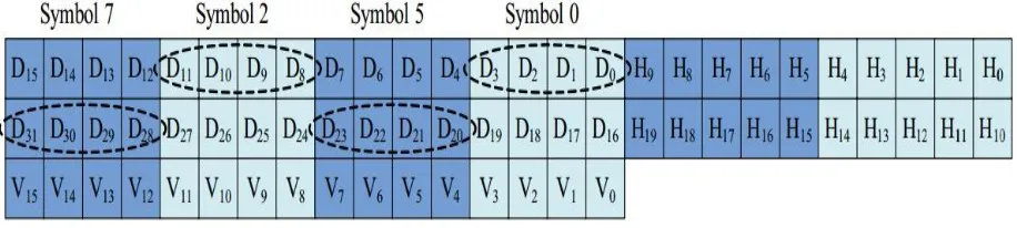
Fig. 2 Logical representation of 32-bit DMC code. Here, each symbol is regarded as a decimal integer
(m = 4) each. The cells numbered from H0 to H19 are horizontal check bits and from V0 to V15 are vertical check bits.
The maximum correction capability of DMC codes and the number of redundant bits are different when different values for k and m are chosen. For example, if k = 2x2 and m = 8, it can correct only one error and the number of redundant bits are 40. If k = 4x4 and m = 2, it can correct three errors and the number of redundant bits are reduced to 32. However, if k = 2x4 and m = 4, it can correct five errors and the number of redundant bits are 36. Therefore, the values of k and m should be selected carefully.
The following equations represent the decimal integer addition to find the horizontal check bits. H[4:0] = symbol2 + symbol0
H[9:5] = symbol7 + symbol5 H[14:10] = symbol3 + symbol1
H[19:15] = symbol6 + symbol4 ….and so on The following equations are used to compute the vertical check bits.
V0 = D0 ^ D16
V1 = D1 ^ D17 …..and so on
The symbol “ ^ “ indicates binary exclusive OR operation. The horizontal syndrome bits are obtained as follows:
▲H[4:0] = H[4:0]’ – H[4:0]
▲H[9:5] = H[9:5]’ – H[9:5] …..and so on The vertical syndrome bits are obtained as follows:
S0 = V0’ ^ V0
S1 = V1’ ^ V1 ……and so on
The errors can be corrected by D0correct = D0’ ^ S0
The drawback of the existing DMC is that it requires large number of redundant bits which is more than double the information bits. The correction capability of this method is also low. It cannot detect type 3, type 4 and type 5 errors discussed later in section V.
IV. PROPOSED MODIFIED-DMC
In this section, modified-DMC is proposed to enhance memory reliability. This approach uses Hamming codes and decimal algorithm, which increases the error detection and correction capability.
A. Block diagram of proposed modified-DMC:
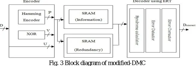
The proposed block diagram of modified- DMC is shown in fig 3. Here, the encoding process may be interpreted as writing the data into SRAM cells and the decoding process as reading the data from SRAM cells. The information bits D are fed to the DMC encoder which computes the horizontal check bits H and vertical check bits V.
Fig. 3 Block diagram of modified-DMC
B.Encoder of modified-DMC:
The proposed modified-DMC encoder is similar to existing DMC encoder but employs Hamming codes for calculating horizontal redundant bits. The circuit of encoder using Hamming encoder and XOR gates is shown in fig 4. First, an N-bit information word is taken as the source data. This N-N-bit word is divided into k-symbols of m-N-bits each which gives N = kxm. These k-symbols are arranged systematically in a k1xk2 2-D matrix form such that k = k1xk2. Here k1
indicates number of rows and k2 indicates number of columns. Second, the horizontal check bits are computed by
employing Hamming codes for each symbol of first row. Here, each symbol is considered as a decimal integer. Third, the vertical check bits are computed by employing binary exclusive OR operation for every column.
Fig. 4 Modified-DMC encoder
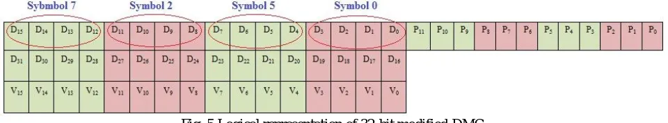
To understand the proposed DMC scheme, implementation of a 32-bit DMC code is explained as an example in fig 5. The cells numbered from D0 to D31 are information bits. This 32-bit word (N = 32) is divided into eight symbols (k = 8)
of 4 bits (m = 4) each. The cells numbered from P0 to P11 are horizontal check bits and from V0 to V15 are vertical check
bits. The maximum correction capability and the number of redundant bits are different when different values for k and m are chosen. For example, if k = 2x4 and m = 4, it can correct maximum of 16-bit errors and the number of redundant bits are 28. Therefore, the values of k and m should be selected carefully.
Fig. 5 Logical representation of 32-bit modified-DMC
The horizontal redundant bits are calculated for all the symbols in only one row. The following equations represent the Hamming equations to calculate the horizontal check bits.
P0 = D3 ^ D1 ^ D0
P1 = D3 ^ D2 ^ D0
P2 = D3 ^ D2 ^ D1 …….and so on
The following equations are used to compute the vertical check bits. V0 = D0 ^ D16
V1 = D1 ^ D17 ……… and so on
The symbol “ ^ “ indicates binary exclusive-OR operation.
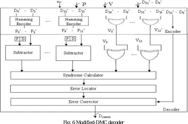
C.Decoder of modified-DMC
In the decoding process, we need to detect the errors if any and correct them accordingly. Here foremost step is using encoder re-use technique. The received information bits D’ are applied to the in-built encoder block in the decoder circuit to obtain the horizontal check bits P0’ to P11’ and vertical check bits V0’ to V15’.The schematic of the decoding
circuit is shown in fig 6.
vertical syndrome bits. The non-zero horizontal syndrome bits indicates error detection and the non-zero vertical syndrome bits gives the location of errors. These errors are corrected by error corrector block using xor operations. The horizontal syndrome bits are obtained as follows:
▲ P0P1P2D3D2D1D0 = P0P1P2D3D2D1D0’ – P0P1P2D3D2D1D0
▲ P3P4P5D7D6D5D4 = P3P4P5D7D6D5D4’ – P3P4P5D7D6D5D4 ….and so on
The vertical syndrome bits are obtained as follows: S0 = V0’ ^ V0
S1 = V1’ ^ V1 …….and so on
The errors can be corrected by D0correct = D0’ ^ S0 … and so on
Fig. 6 Modified-DMC decoder
The table I shows the functions of En signal. The enable signal En can be used to determine whether the encoder needs to be a part of the decoder. Hence, the En signal distinguishes the encoder from the decoder and it will be under the control of the write and read signals in memory.
Table I
Functions of Enable signal
Extra circuit En signal Function Read signal Write signal
Encoder 0 1 Encoding 1 0 Compute syndrome bits
V.ADVANTAGE OF MODIFIED-DMC
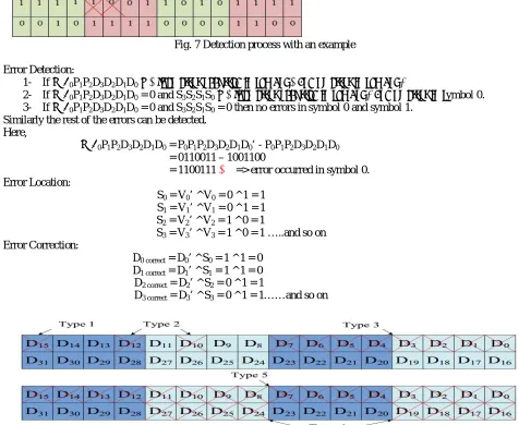
Fig. 7 Detection process with an example
Error Detection:
1- If ▲P0P1P2D3D2D1D0≠ 0 then error occurred in symbol 0 and no error in symbol 1.
2- If ▲P0P1P2D3D2D1D0 = 0 and S3S2S1S0≠ 0 then error occurred in symbol 1 and no error in symbol 0.
3- If ▲P0P1P2D3D2D1D0 = 0 and S3S2S1S0 = 0 then no errors in symbol 0 and symbol 1.
Similarly the rest of the errors can be detected. Here,
▲P0P1P2D3D2D1D0 = P0P1P2D3D2D1D0’ - P0P1P2D3D2D1D0
= 0110011 – 1001100
= 1100111 ≠ 0 => error occurred in symbol 0. Error Location:
S0 = V0’ ^ V0 = 0 ^ 1 = 1
S1 = V1’ ^ V1 = 0 ^ 1 = 1
S2 = V2’ ^ V2 = 1 ^ 0 = 1
S3 = V3’ ^ V3 = 1 ^ 0 = 1 …..and so on
Error Correction:
D0 correct = D0’ ^ S0 = 1 ^ 1 = 0
D1 correct = D1’ ^ S1 = 1 ^ 1 = 0
D2 correct = D2’ ^ S2 = 0 ^ 1 = 1
D3 correct = D3’ ^ S3 = 0 ^ 1 = 1……and so on
Fig. 8 Type 1 is a single error, type 2 is an inconsecutive error in two consecutive symbols, type 3 is a consecutive error in two consecutive symbols, type 4 is an inconsecutive error in two inconsecutive symbols, and type 5 is a consecutive
error in four consecutive symbols.
(1) The decimal integer addition of bits in symbols 0 and 2 is equal to 2m-1 (2) All the bits in symbols 0 and 2 are upset
The proposed modified-DMC successfully detects and corrects type 3 and type 4 errors provided no two errors occur in the same column.
VI. RESULT AND DISCUSSION
The complete proposed method is coded in VHDL. The design was simulated using ModelSim and Xilinx ISE is used to estimate the area required for the design, power consumption and delay overhead. From fig 7, it can be observed that the encoder is re-used for obtaining the syndrome bits in the decoder. Therefore, the overall circuit area for the implementation of the proposed method is reduced.
Table II
Area, Power, Delay analysis for 32-bit data
TECHNIQUE Area (Gate count) Power (mW) Delay (ns)
Modified DMC 65970 84 8.876
DMC 74857 103 11.29
The area, power and delay overhead analysis of encoder and decoder circuits are given in table II. It shows the area in terms of number of gates required to implement the design, the total estimated power consumption in mW and the overall delay to get the output when the input is applied to the design.
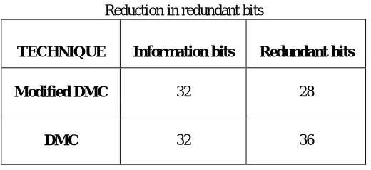
Table III
Reduction in redundant bits
TECHNIQUE Information bits Redundant bits
Modified DMC 32 28
DMC 32 36
The differences in the number of redundant bits required are given in table III. It shows that for 32-bit information the proposed method requires 28 redundant bits while the existing method requires 36 bits. From this table, it can be observed that the proposed modified-DMC technique reduced the number of redundant bits required to detect and correct the MCUs.
VII.CONCLUSION
REFERENCES
1. Jing Guo, Liyi Xiao, “Enhanced memory reliability against multiple cell upsets using decimal matrix code,” IEEE Transactions on VERY LARGE SCALE INTEGRATION (VLSI) SYSTEMS, vol. 22, No.1, January 2014.
2. A. Sanchez-Macian, P. Reviriego, and J. A. Maestro, “Hamming SEC-DAED and extended hamming SEC-DED-TAED codes through selective shortening and bit placement” IEEE Trans. Device Mater. Rel., to be published.
3. R. Naseer and J. Draper, “Parallel double error correcting code design to mitigate multi-bit- upsets in SRAMs,” in Proc. 34th Eur. Solid-State
Circuits, Sep. 2008,, pp. 222-225.
4. G. Neuberger, D. ?L. Kastensmidt, and R. Reis, “An automatic technique for optimizing Reed-Solomon codes to improve fault tolerance in memories,” IEEE Design Test Comput., vol. 22, no; 1, pp; 50-58, Jan.-Feb. 2005.
5. R. C. Baumann, “Radiation-induced soft errors in advanced semiconductor technologies,” IEEE Trans. Device Mater. Reliab., vol. 5, no. 3, pp. 301-316, 2005.
6. E. Ibe, H. Taniguchi, Y. Yahagi, K. Shimbo, and T. Toba, “Impact of scaling on neutron induced soft error in SRAMs from an 250 nm to a 22 nm design rule,” IEEE Trans. Electron Devices, vol. 57, no. 7, pp. 1527-1538, Jul. 2010.
7. Wakerly, J. F. Error detecting codes, self-checking circuits and applications. New York: North-Holland, 1978. 8. A. D. Houghton, The Engineer’s Error Coding Handbook. London, U.K.: Chapman and Hall, 1997.
9. S. Baeg, S. Wen, and R. Wong, “Interleaving distance selection with a soft error failure model,” IEEE Trans. Nucl. Sci., vol. 814-822, Apr. 2010.
10. A. Dutta and N. A. Touba, “Multiple bit upset tolerant memory using a selective cycle avoidance based SEC-DED-DAEC code,” in Proc. IEEE VLSI Test Symp. (VTS), 2007, pp. 349-354.