Design and Implementation of 256-bit Ripple Carry
Adder Design
A.Anandha Raja
1, S.Jeeva
2, P.Karthikeyan
3N.Karthikeyan
4, D.Praveen kumar
51
Assistant Professor, Department of ECE,SNS College of Technology , Coimbatore, (India)
2,3,4
Student, Department of ECE,SNS College of Technology , Coimbatore, (India)
5
SNS College of Technology, Coimbatore, (India)
ABSTRACT
Design and implementation of high speed and less area designs plays a dynamic role in many industrial applications and/or research areas of design in VLSI. Current technology is attenuation to micrometer from nanometer technology in order to meet these design issues. Ripple carry adder is one of the designs which are used in many applications like DSP’s, ALU’s, subtractions and high speed multiplications. In the modern ripple carry adder designs, the main design area is focus on the power factor and not on the high speed operation. Similarly the performance of any design is to be increased to a great extent by improving the speed of operation. So our paper mainly focuses on the high speed 256 bit ripple carry adder design. In our paper an analysis of 256 bit Ripple Carry adder which is designed using Xilinx software.
Keywords: Full Adder, Ripple Carry Adder (RCA), Xilinx
I.
INTRODUCTION
Basic Binary Adder circuit can be made from standard AND and Ex-OR gates allowing us to “ADD” together two single bit binary numbers A and B. The addition of these two digits produces an output called the SUM of the addition and a second output called the CARRY or Carry-out, (COUT) bit according to the rules for binary
addition. One of the main uses for the Binary Adder is in arithmetic and counting circuits.
Today world trends is based on Complementary Symmetry Metal Oxide Semiconductor (CMOS) for integrating more operations within the given area of single chip. Past few years it is seen that there is tremendous use of nano-scale technologies for industrial production of high performance Integrated Circuits(IC) and the 2 important characteristics of CMOS devices which are very important are noise immunity and less static power consumption.
II. RIPPLE CARRY ADDER
Multiple full adder circuits can be cascaded in parallel to add an N-bit number. For an N- bit parallel adder, there must be N number of full adder circuits. A ripple carry adder is a logic circuit in which the carry-out of each full adder is the carry in of the succeeding next most significant full adder. It is called a ripple carry adder because each carry bit gets rippled into the next stage.
In a ripple carry adder the sum and carry out bits of any half adder stage is not valid until the carry in of that stage occurs. Propagation delays inside the logic circuitry is the reason behind this. Propagation delay is time elapsed between the application of an input and occurrence of the corresponding output. Consider a NOT gate, When the input is “0” the output will be “1” and vice versa. The time taken for the NOT gate’s output to become “0” after the application of logic “1” to the NOT gate’s input is the propagation delay here.
Similarly the carry propagation delay is the time elapsed between the application of the carry in signal and the occurrence of the carry out (COUT) signal.
III.
RIPPLE CARRY ADDER
DESIGN USINGNAND GATE
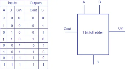
Full adder is a logic circuit that adds two input operand bits plus a Carry in bit and outputs a Carry out bit and a sum bit. The Sum out (SOUT) of a full adder is the XOR of input operand bits A, B and the Carry in (CIN) bit.
Truth table and schematic of a single bit Full adder is shown below.
Figure1: Single bit full adder Truth table and Schematic.
Full adder circuit was designed by using NAND gates and schematic is shown below.
Similarly Circuit diagram of a 4-bit ripple carry adder is shown below.
Figure 3: Schematic of 4-bit ripple carry adder
IV.
RIPPLE CARRY ADDER
DESIGN USING XILINX
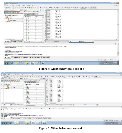
The first step simulation of our design is typically performed to verify RTL (behavioral) code and to confirm that the design is functioning as intended. This code process are shown in below diagrams.
Figure 4: Xilinx behavioral code of a
V.
RIPPLE CARRY ADDER: SIMULATION OUTPUT USINGXILINX
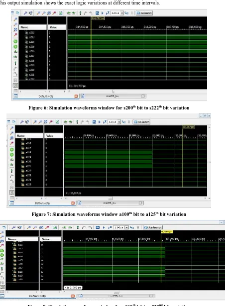
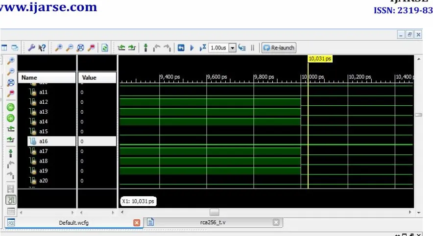
The results of the simulation process of 256-bit Ripple Carry Adder Designis shown in below diagrams. This output simulation shows the exact logic variations at different time intervals.
Figure 6: Simulation waveforms window for s200th bit to s222th bit variation
Figure 7: Simulation waveforms window a100th bit to a125th bit variation
Figure 9: Simulation waveforms window a010th bit to a025th bit variation at different period
Figure 10: Simulation waveforms window for b020th bit to b030th bit variation
VI.
CONCLUSION
In this paper the result concludes that a compact and basic 256 bit designed using Xilinx simulation software, which isshown with their design topology, detailed ease of verification.
Based on the designing and results of adder proved to be more efficient than 128 bit adder.
ACKNOWLEDGMENT
REFERENCES
[1] Dan Wang. "Novel low power full adder cells in 180nm CMOS technology", 2009 4th IEEE Conference on Industrial
Electronics and Applications, 05/2009.Yingtao Jiang, Abdulkarim Al-Sheraidah, Yuke Wang, Edwin Sha, and Jin-Gyun Chung, “A Novel Multiplexer- Based Low-Power Full Adder” IEEE Transaction on circuits and systems-II:
Express Brief,Vol. 51, No. 7,p-345, July-2004.
[2] S.Usha, T.Ravi, “Design of 4-Bit Ripple Carry Adder Using Hybrid 9TFull Adder”, International Conference on Circuit,
Power and Computing Technologies [ICCPCT], 2015. Po-Ming Lee, Chia-Hao Hsu, and Yun-Hsiun Hung, “Novel 10-T full adders realized by GDI structure”, IEEE International Symposium on Integrated Circuits (ISIC-2007).
[3] S.Archana, G.Durga, “Design of Low Power and High Speed Ripple Carry Adder”, International Conference on
Communication and Signal Processing, April 3 -5, 2014.
[4] K. Yano, K. Yano, T. Yamanaka, T. Nishida, M. Saito, K. Shimohigashi, and A. Shimizu, “A 3.8 ns CMOS 16 *16-b
multiplier using complementary pass-transistor logic,” IEEE J. Solid-State Circuits , vol. 25, no. 2, pp. 388–395, Apr.
1990.
[5] M. Suzuki, M. Suzuki, N. Ohkubo, T. Shinbo, T. Yamanaka, A. Shimizu, K. Sasaki, and Y. Nakagome, “A 1.5 ns 32-b
CMOS ALU in double pass-transistor logic,” IEEE J. Solid-State Circuits , vol. 28, no. 11, pp. 1145–1150, Nov. 1993.
[6] R. Zimmerman and W. Fichtner, “Low-powerogic styles: CMOS versus pass-transistor logic,” IEEE J. Solid-State
Circuits ,vol. 32, no. 7, pp. 1079–1090, Jul. 1997.
[7] C. Chang, J. Gu, and M. Zhang, “A review of 0.18- m full adder performances for tree structured arithmetic circuits,”
IEEETrans. Very Large Scale Integr. (VLSI) Syst., vol. 13, no. 6, pp. 686–695, Jun. 2005.
[8] S. Goel, A. Kumar, and M. Bayoumi, “Design of robust, energy-efficient full adders for deep-sub micrometer design
using hybrid-CMOS logic style,” IEEE Trans. Very Large Scale Integration. (VLSI) Syst., vol. 14, no. 12, pp. 1309–
1320, Dec. 2006.
[9] S. Agarwal, V. K. Pavankumar, and R. Yokesh, “Energy efficient high performance circuits for arithmetic units,” in