WANG, JUN. Design, Characterization, Modeling and Analysis of High Voltage Silicon Carbide Power Devices. (Under the direction of Dr. Alex Q. Huang).
This research focuses on the design, characterization, modeling and analysis of high
voltage Silicon Carbide (SiC) metal-oxide-semiconductor field effect transistors (MOSFET),
insulated gate bipolar transistors (IGBT) and emitter turn-off thyristors (ETO) to satisfy
the stringent requirements of advanced power electronic systems. The loss information,
frequency capability and switching ruggedness of these 10-kV SiC power devices are studied
extensively in order to provide their application prospects in solid-state transformers (SST).
Among 10-kV SiC power devices, SiC MOSFETs are of the greatest interest due
to their lower specific on-resistance compared to silicon MOSFETs, and their inherently
fast switching speed due to their majority carrier conduction mechanism. Therefore, 10-kV
SiC MOSFETs are studied first in this dissertation. The characterization, modeling and
analysis of 10-kV SiC MOSFETs were investigated extensively. The low losses and high
switching frequency of 10-kV SiC MOSFETs were demonstrated in characterization study
and a 4-kV 4 kW boost converter.
The on-resistance of SiC MOSFETs increases rapidly with increased junction
tem-perature and blocking voltage. This makes their conduction losses possibly unacceptable
for applications where high DC supply voltages (≥10-kV) and high temperature operation are used. This warrants the development of SiC bipolar devices (IGBTs and thyristors) to
achieve smaller conduction losses due to the conductivity modulation of their thick drift
layers, especially at elevated temperatures. Therefore, design, characterization and
The device exhibited a differential on-resistance of 26 mΩ·cm2at a collector current density of 100 A/cm2 at room temperature. The SiC IGBT showed a turn-off time of 1 µs in an inductive load circuit with a DC-link voltage of 4-kV and a collector current density of
150 A/cm2 at room temperature. The possible approaches to achieve a better performance
trade-off between forward voltage drop and turn-off energy loss were investigated using
numerical simulations.
In order to maintain the superior conduction characteristics of SiC GTO and
im-prove its dynamic characteristics, high voltage SiC ETO was developed. The experimental
demonstration of the world’s first 4.5-kV SiC ETO prototype shows a four time higher
switching frequency and a much higher power density than its silicon counterparts.
Nu-merical simulations and theoretical analysis have been carried out to show the potentially
improved performance of 10-kV SiC ETO. The results show that 10-kV SiC n-type ETO
has much better performance trade-off than that of the p-type ETO due to a smaller
cur-rent gain of the lower bipolar transistor. Further improvement of SiC ETO can be done by
developing SiC n-type GTO.
The characteristics and losses of 10-kV SiC MOSFET, p-IGBT and ETO were
compared using the experimental measurement results, PSPICE simulations and numerical
simulations. Using the extracted loss information of SiC power devices and method of loss
calculation in SST, the frequency capability of these 10-kV SiC power devices in a 20 kVA
SST was investigated and compared in the same power loss density of 300 W/cm2 and
mm2. Using 10-kV SiC MOSFET, a switching frequency of more than 20 kHz in the SST
can be achieved by choosing an optimum chip size of the SiC MOSFET, which can greatly
by Jun Wang
A dissertation submitted to the Graduate Faculty of North Carolina State University
in partial fullfillment of the requirements for the Degree of
Doctor of Philosophy
Electrical Engineering Raleigh, North Carolina
2010
APPROVED BY:
Dr. B. Jayant Baliga Dr. Subhashish Bhattacharya
Dr. Alex Q. Huang Dr. Doug Barlage
BIOGRAPHY
Jun Wang was born in China in 1979. He received a B.S. degree in electrical engineering at
Huazhong University of Science and Technology, Wuhan, China in 2000. He received the
M.S. degree at Chinese Academy of Sciences, Beijing, China in 2003. In 2005, he received
the M.E. degree in Electrical Engineering department at University of South Carolina. His
research activities from 2000 to 2005 focused on the fabrication and characterization of
III-nitrides UV detectors and LEDs.
From June 2005, he started working toward the Ph.D. degree at the
Semicon-ductor Power Electronics Center (renamed as Future Renewable Electric Energy Delivery
and Management (FREEDM) Systems Center in 2008) at North Carolina State University,
Raleigh, NC. His research interests include the design, characterization, modeling and
anal-ysis of high voltage 4H-SiC power devices, including junction barrier Schottky (JBS) diodes,
PiN diodes, metal-oxide-semiconductor field effect transistors (MOSFET), insulated gate
bipolar transistors (IGBT), thyristors, emitter turn-off thyristors (ETO) and base resistance
controlled thyristors (BRT).
He had a summer internship in Cree Inc. in North Carolina in 2007, working on
the characterization and modeling high voltage SiC MOSFETs. In the summer of 2009,
he served as a research participant in an Advanced Short Term Research Opportunity
(ASTRO) program at Oak Ridge National Laboratory (ORNL) in Tennessee, analyzing
600V GaN heterojunction field effect transistors (HFETs) on Si substrates for applications
in motor drive inverters of electric vehicles.
He has authored or coauthored over 20 technical papers and conference
ACKNOWLEDGMENTS
I would like to thank my advisor, Dr. Alex Q. Huang, for his guidance, support and
encouragement over the course of my graduate study and research at North Carolina State
University. His knowledge, vision and creative thinking have been a source of inspiration.
His suggestions on various subjects provided a valuable source of ideas that will benefit
me for years. Besides his direct supervision in the research work, his virtue of patience in
teaching and devotion in research set a model of a scholar for me. It was an invaluable
learning experience to be one of his graduate students.
In the last two years of my study, Dr. B. Jayant Baliga gave me excellent
super-vision on my research. His brilliant ideas and illuminating suggestions helped me a lot. I
am impressed by his broad thoughts and diligent attitude.
I am also grateful to have Dr. Doug Barlage, Dr. Subhashish Bhattacharya as my
doctoral committee members. Their encouragement and expertise helped me throughout
my graduate study. I appreciate that Dr. Xiangwu Zhang and Dr. Daniel J. Lichtenwalner
attended my PhD exams as my graduate representatives.
I would like to thank Dr. Qingchun (Jon) Zhang in Cree Inc.. His creativity and
intelligence drove the in-depth SiC IGBT study. The helpful discussion with him has played
an important role in the completion of this work. I would like to thank Robert Callanan
and Fatima Husna in Cree Inc.. Their instruction and suggestions help me a lot in the
testing and SPICE modeling of SiC MOSFETs. I appreciate the support of Dr. Anant
Agarwal and Dave Grinder in Cree in my research work.
It has been a great pleasure to work with the excellent staffs and students at
conducive to work, due to the presence of friendly and cooperative graduate students and
staff. I would like to thank Ms. Yan Gao, Mr. JeeSung Jung, Mr. Yang Gao, Mr. Tiefu
Zhao, Mr. Gangyao Wang, Mr. Yu Du, Mr. Jun Li, Mr. Xiaohu Zhou, Mr. Yu Liu, Mr.
Edward Van Brunt, Mr. Woongje Sung, Mr. Xin Zhou, Mr. Jiwei Fan, Mr. Jinseok Park,
Mr. Xiaoming Duan and Mr. Bin Chen for many enlightening discussions and exchange of
thoughts. I appreciate the help from Mrs Colleen Reid, Mr. Anousone Sibounheuang and
Mr. Seth Crossno during my study in SPEC.
I would like to thank my parents for being the ultimate source of strength and
encouragement throughout my academic career and personal life. Special thanks to my
wife, Wei Wang, who has always been there with her love, understanding, and support over
TABLE OF CONTENTS
LIST OF TABLES . . . viii
LIST OF FIGURES . . . ix
1 Introduction . . . 1
1.1 Background . . . 1
1.2 Physical and electrical properties of SiC . . . 5
1.3 Challenges of research . . . 10
1.4 Outline of dissertation . . . 11
2 Theoretical Capability of SiC Power Devices . . . 15
2.1 Introduction . . . 15
2.2 Theoretical specific on-resistance of SiC unipolar devices . . . 15
2.3 Theoretical frequency capability of SiC unipolar devices . . . 18
2.3.1 Brief introduction of HMFOM . . . 19
2.3.2 Theoretical frequency capability . . . 21
2.4 Theoretical dynamic avalanche breakdown of 4H-SiC bipolar devices . . . . 23
2.5 Summary . . . 29
3 Characterization, SPICE Modeling and Analysis of 10-kV 4H-SiC MOS-FET . . . 31
3.1 Introduction of power MOSFETs . . . 31
3.1.1 Operation principal . . . 33
3.1.2 Internal capacitances . . . 34
3.1.3 Switching performance . . . 35
3.2 Status of SiC MOSFETs . . . 41
3.3 Characteristic study of a 10kV 5A SiC MOSFET . . . 44
3.3.1 DC characteristic study . . . 44
3.3.2 Transient characteristic study . . . 52
3.4 Behavioral SPICE model of SiC MOSFETs . . . 56
3.4.1 SPICE model infrastructure . . . 56
3.4.2 DC parameter extraction and validation . . . 59
3.4.3 AC model infrastrurcture and parameter extraction . . . 64
3.4.4 Validation of transient characteristics of a 10kV 5A SiC MOSFET . 66 3.5 Validation of SPICE model of a 10kV 10A SiC MOSFET . . . 71
3.6 10 kV SiC MOSFET based boost converter . . . 73
4 Design and Characterization of a 10-kV SiC IGBT . . . 86
4.1 Introduction of IGBTs . . . 86
4.2 Status of SiC IGBTs . . . 90
4.3 Device design and fabrication . . . 91
4.4 Results and discussion . . . 93
4.4.1 Blocking J-V characteristics . . . 93
4.4.2 On-state J-V characteristics . . . 94
4.4.3 Role of CEL layer in IGBT and device geometry optimization . . . . 97
4.4.4 Transient characteristics . . . 101
4.4.5 Reverse bias safe operating area (RBSOA) . . . 104
4.4.6 Effect of carrier lifetime in drift region . . . 106
4.4.7 Optimization of the buffer layer . . . 107
4.5 Conclusion . . . 109
5 Design, Optimization and Analysis of High Voltage SiC ETOs. . . 111
5.1 Introduction of thyristors . . . 111
5.2 Status of SiC thyristors . . . 114
5.3 Introduction of ETOs . . . 115
5.4 Motivation of SiC ETO . . . 119
5.5 Experiment details and results of a 4.5-kV SiC p-type ETO . . . 120
5.6 Result discussions and further improvements in 10-kV SiC ETOs . . . 129
5.6.1 Comparison of n-type and p-type SiC ETOs . . . 130
5.6.2 Effect of buffer layer to the performance trade-off of 10-kV SiC ETOs 134 5.6.3 Effect of drift layer Carrier lifetime on the performance trade-off of 10-kV SiC n-type ETOs . . . 136
5.6.4 Reverse bias safe operating area (RBSOA) of 10-kV SiC n-type ETO 137 5.7 Summary . . . 138
6 Comparison of 10-kV SiC Power Devices in Solid-State Transformer . . . 141
6.1 Introduction . . . 141
6.2 Loss Comparison of 10-kV SiC Power Devices . . . 142
6.2.1 Comparison of forward I-V characteristics . . . 142
6.2.2 Comparison of turn-off loss . . . 144
6.3 Comparison of 10-kV SiC devices in solid-state transformer . . . 146
6.3.1 Introduction of solid-state transformer . . . 146
6.3.2 Loss calculation of 10-kV SiC devices in solid-state transformer . . . 149
6.3.3 Frequency capability of 10-kV SiC power devices in SST . . . 150
6.3.4 Effect of chip size of 10-kV SiC power devices to their frequency ca-pability in SST . . . 153
6.4 Summary . . . 158
7 Summary and Future Work . . . 159
7.1 Major contributions . . . 159
Bibliography . . . 166
LIST OF TABLES
Table 1.1 Comparison of electrical properties of SiC and Si . . . 8
Table 1.2 Comparison of the normalized figures of merits of SiC and Si . . . 10
Table 3.1 Extracted DC parameters . . . 59
Table 3.2 Extracted parameters related to threshold voltage . . . 61
Table 3.3 Extracted parameters related to transconductance . . . 62
Table 3.4 Extracted parameters related to on-state resistance . . . 63
Table 3.5 Extracted parameters related to capacitances of the SiC MOSFET . . . 66
Table 4.1 Physical models and parameters used in simulations . . . 98
Table 6.1 Comparison of 10-kV SiC MOSFET, p-IGBT and ETO in the AC/DC rectifier of the 20 kVA SST . . . 152
Table 6.2 Comparison of 10-kV SiC MOSFET, p-IGBT and ETO in the hard switching DC/DC converter of the 20 kVA SST . . . 152
LIST OF FIGURES
Figure 1.1 Applications of silicon power devices [1] . . . 2
Figure 1.2 Power range of commercially available high power semiconductor devices [2] 3
Figure 1.3 Power and frequency capabilities of today’s silicon power devices . . . 4
Figure 1.4 Comparison of 10 kV SiC MOSFETs based solid state transformer to con-ventional transformer . . . 5
Figure 1.5 The basic structural unit in SiC, the tetragonal bonding of a carbon atom with four nearest silicon neighbors [5] . . . 6
Figure 1.6 Stacking orders along c-axis for 3C-, 4H-, and 6H-SiC. Open and closed circles represent Si and C atoms, respectively [5] . . . 7
Figure 2.1 Comparison of drift layer thickness of Si and SiC power devices as a function of blocking voltage . . . 18
Figure 2.2 Comparison of theoretical specific on-resistance of Si and SiC unipolar de-vices at room temperature . . . 19
Figure 2.3 Calculated frequency capabilities of Si and SiC unipolar devices vs. their blocking voltage at specified conditions. . . 23
Figure 2.4 Schematic illustration of dynamic avalanche of SiC bipolar devices . . . 24
Figure 2.5 Current density vs. onset voltage of dynamic avalanche breakdown of the 10-kV SiC and Si n-type bipolar devices . . . 27
Figure 2.6 Current density vs. onset voltage of dynamic avalanche breakdown of 10-kV SiC n-type and p-type bipolar device. . . 29
Figure 3.1 Cross-section view of a basic Si n-channel power MOSFET cell structure . . 32
Figure 3.2 Output characteristic of a basic Si n-channel power MOSFET cell structure 33
Figure 3.3 Internal capacitances of a basic Si n-channel power MOSFET cell structure 34
Figure 3.5 Circuit used for transient analysis of a power MOSFET . . . 36
Figure 3.6 Turn-on transient waveforms of a power MOSFET . . . 37
Figure 3.7 Equivalent circuit of the clamped inductive load test circuit of a power MOSFET in the stages of turn-on transient . . . 38
Figure 3.8 Turn-off transient waveforms of a power MOSFET . . . 40
Figure 3.9 Simplified cross section of a 10-kV SiC MOSFET . . . 45
Figure 3.10 Measured forward I-V characteristics of a 10-kV 4H-SiC MOSFET at room temperature . . . 46
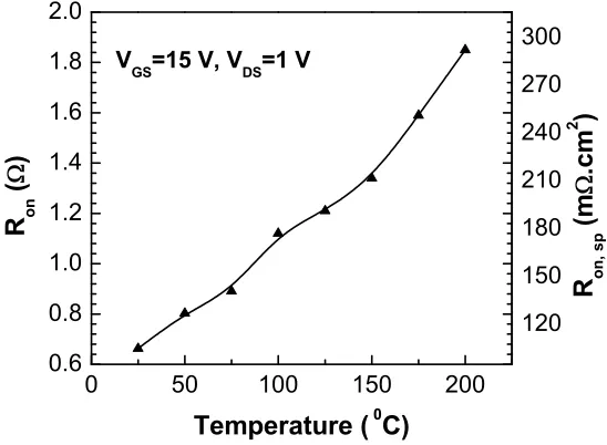
Figure 3.11 Measured on-resistance of a 10-kV 4H-SiC MOSFET as a function of junction temperature . . . 47
Figure 3.12 Measured transfer curve of a 10-kV 4H-SiC MOSFET as a function of tem-perature . . . 47
Figure 3.13 Threshold voltage of a 10-kV 4H-SiC MOSFET as a function of temperature 48
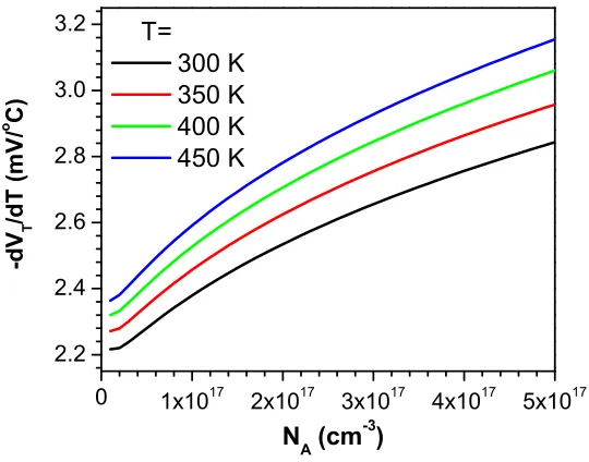
Figure 3.14 Effect of p-well doping concentration of a 10-kV 4H-SiC MOSFET on the rate of change of threshold voltage with doping concentration of p-well surface in elevated temperatures. . . 51
Figure 3.15 Transconductance and transconductance parameter of a 10-kV 4H-SiC MOS-FET as a function of temperature . . . 51
Figure 3.16 Schematic circuit diagram of a resistive load test circuit for a 10 kV SiC MOSFET . . . 52
Figure 3.17 Switching waveforms of 10 kV 4H-SiC MOSFET in resistive load circuit with RG = 1 kΩ and VBU S=1 kV. . . 53
Figure 3.18 Switching waveforms of 10 kV 4H-SiC MOSFET in resistive load circuit with RG= 2Ω and VBU S=1 kV . . . 54
Figure 3.19 Switching energy losses of 10 kV 4H-SiC MOSFET vs. load current in resistive load circuit . . . 54
Figure 3.20 Schematic circuit diagram of a inductive load test circuit for a 10 kV SiC MOSFET . . . 55
Figure 3.22 Measured turn-on energy loss of a 10 kV SiC MOSFET in a clamped induc-tive load circuit . . . 57
Figure 3.23 Measured turn-off energy loss of a 10 kV SiC MOSFET in a clamped inductive load circuit . . . 57
Figure 3.24 Equivalent subcircuit of a SiC power MOSFET . . . 58
Figure 3.25 PSpice simulated and measured output characteristics of a 10 kV SiC MOS-FET at room temperature . . . 60
Figure 3.26 PSpice simulated and measured threshold voltage of a 10 kV SiC MOSFET vs. temperature . . . 61
Figure 3.27 PSpice simulated and measured transfer curve of a 10 kV SiC MOSFET at elevated temperatures. . . 63
Figure 3.28 Measured and PSpice simulated on-resistance of a 10 kV SiC MOSFET as a function of temperature . . . 64
Figure 3.29 Modified switch model for the non-linear CGD of a SiC power MOSFET . . 65
Figure 3.30 PSpice simulated, measured and numerically simulated CGD-VDS curves of
a 10 kV SiC MOSFET . . . 67
Figure 3.31 Measured and PSpice simulated switching waveforms of a 10 kV SiC MOS-FET in a resistive load circuit . . . 68
Figure 3.32 Measured and PSpice simulated switching waveforms of a 10 kV SiC MOS-FET in a clamped inductive load circuit . . . 68
Figure 3.33 Measured and PSpice simulated switching loss of a 10 kV SiC MOSFET in a resistive load circuit with various load currents . . . 69
Figure 3.34 Measured and PSpice simulated turn-on losses of a 10 kV SiC MOSFET in a clamped inductive load circuit . . . 70
Figure 3.35 Measured and PSpice simulated turn-off losses of a 10 kV SiC MOSFET in a clamped inductive load circuit . . . 70
Figure 3.36 Measured and PSpice simulated output characteristics of a 10kV 10A SiC MOSFET at room temperature . . . 71
Figure 3.38 Measured and PSpice simulated transfer characteristics at elevated
temper-ature . . . 72
Figure 3.39 Schematic of the 10-kV SiC MOSFET based boost converter . . . 74
Figure 3.40 Simulated switching waveform of the 10-kV SiC MOSFET in the designed boost converter . . . 75
Figure 3.41 Experimental setup of the 10-kV SiC MOSFET based boost converter . . . . 75
Figure 3.42 Measured switching waveform of the 10-kV SiC MOSFET based boost converter . . . 76
Figure 3.43 Zoomed in switching waveform of the 10-kV SiC MOSFET in the tested boost converter . . . 77
Figure 3.44 Closed loop thermal model for SiC power devices at fixed operation voltage, current and switching frequency. . . 78
Figure 3.45 Measured on-resistance of the 10-kV SiC MOSFET in pulse mode and DC mode vs. ambient temperature . . . 79
Figure 3.46 Extracted DC thermal resistance of the 10-kV SiC MOSFET in the boost converter . . . 80
Figure 3.47 Relationship between the measured power efficiency and the switching fre-quency of the boost converter . . . 81
Figure 3.48 Relationship between the measured power efficiency and the load current of the boost converter . . . 82
Figure 3.49 Relationship between the measured power loss and the load current of the boost converter . . . 83
Figure 3.50 Relationship between the measured power loss of the SiC MOSFET and the input voltage of the boost converter . . . 84
Figure 4.1 Cross section of a basic IGBT cell structure . . . 88
Figure 4.2 Schematic of forward conduction of a basic IGBT cell . . . 88
Figure 4.3 Equivalent circuit of a n-channel IGBT . . . 89
Figure 4.4 Cross section of the IGBT cell structure . . . 93
Figure 4.6 On-state characteristics of IGBTs at 25oC and 200oC . . . 95
Figure 4.7 Hole inversion channel mobility dependence on the gate-anode voltage . . . . 95
Figure 4.8 Room temperature forward I-V characteristics in a BJT test structure . . . . 96
Figure 4.9 The effect of JFET length to the forward voltage drop at 50 A/cm2 current density and the maximum electric field in the gate oxide at zero gate voltage . . . 99
Figure 4.10 Comparison of electron distribution profile along the vertical cut in the center of the JFET region. . . 100
Figure 4.11 The dependence of blocking voltage capability and maximum electric field in oxide at zero gate voltage on the doping concentration of CEL . . . 100
Figure 4.12 C-V curves of a SiC p-IGBT . . . 101
Figure 4.13 Clamped inductive load switching waveforms of a SiC p-IGBT . . . 102
Figure 4.14 Clamped inductive load switching waveforms of a SiC p-IGBT under high SOA condition . . . 103
Figure 4.15 Clamped inductive load switching waveforms of a SiC p-IGBT under high SOA condition . . . 104
Figure 4.16 Simulated RBSOA and experimental turn-off trajectory of the SiC p-channel IGBT . . . 105
Figure 4.17 Forward voltage drop and turn-off energy trade-off curve at various carrier lifetimes in drift layer . . . 107
Figure 4.18 Trade-off curve of forward voltage drop and turn-off energy loss at various buffer layer parameters. The minority carrier lifetime in the drift layer is 450 ns . . 108
Figure 4.19 Trade-off curve of forward voltage drop and turn-off energy loss at various buffer layer parameters. The minority carrier lifetime in the drift layer is 2 us . . . . 109
Figure 5.1 Cross section of a basic thyristor cell structure . . . 112
Figure 5.2 Equivalent circuit of a n-type ETO . . . 118
Figure 5.3 Evolution of ETOs . . . 118
Figure 5.4 4.5-kV SiC ETO prototype . . . 121
Figure 5.6 Circuit symbol of SiC ETO . . . 123
Figure 5.7 Blocking characteristics of the SiC GTO at room temperature . . . 124
Figure 5.8 Forward I-V characteristics of the SiC GTO at elevated temperature . . . 125
Figure 5.9 Forward I-V characteristics of the SiC ETO at elevated temperature . . . 125
Figure 5.10 Turn-off waveforms of the 4.5-kV SiC ETO . . . 127
Figure 5.11 4.5-kV SiC ETO turn-off characteristics under a high SOA condition . . . 129
Figure 5.12 Simulated on-state characteristics of the 10-kV SiC ETO at 25 oC and 200 oC . . . 132
Figure 5.13 Simulated switching waveforms of the 10-kV SiC n-type ETO in a clamped inductive load circuit at 25oC . . . 133
Figure 5.14 Simulated switching waveforms of the 10-kV SiC p-type ETO in a clamped inductive load circuit at 25oC . . . 133
Figure 5.15 Theoretical turn-off loss versus forward voltage drop for the 10-kV SiC ETO with various buffer layer doping densities. . . 135
Figure 5.16 Theoretical turn-off loss versus forward voltage drop for the 10-kV SiC n-type ETO with various drift layer carrier lifetime and buffer layer doping concentration in the SiC GTO . . . 137
Figure 5.17 Dynamic avalanche breakdown of the 10-kV SiC ETO and its comparison with the turn-off I-V trajectory under normal operation conditions and Si ETO . . 139
Figure 6.1 Forward I-V curves of 10-kV SiC MOSFET, p-IGBT and ETO at room temperature . . . 143
Figure 6.2 Forward I-V curves of 10-kV SiC MOSFET, p-IGBT and ETO at 125oC . 143 Figure 6.3 Turn-off energy loss density of a 10-kV SiC MOSFET vs. load current density at 125oC . . . 144
Figure 6.4 Turn-off energy loss density of a 10-kV SiC p-IGBT vs. load current density at 125 oC . . . 145
Figure 6.6 Turn-off energy loss density of a 10-kV SiC MOSFET, p-IGBT and ETO vs. load current density at 125oC . . . 147
Figure 6.7 Topology of a 20 kVA solid-state transformer . . . 148
Figure 6.8 Schematic current waveform of a main switch device in an AC/DC rectifier149
Figure 6.9 Maximum frequencies of 10-kV SiC MOSFET, p-IGBT and ETO in the AC/DC rectifier of the 20 kVA solid-state transformer vs. their chip size . . . 154
Figure 6.10 Conduction losses of 10-kV SiC MOSFET, p-IGBT and ETO in the AC/DC rectifier of the 20 kVA solid-state transformer vs. their chip size . . . 156
Figure 6.11 Maximum frequencies of 10-kV SiC MOSFET, p-IGBT and ETO in the hard switching DC/DC converter of the 20 kVA solid-state transformer vs. their chip size . . . 157
Figure 6.12 Maximum frequencies of 10-kV SiC MOSFET, p-IGBT and ETO in the soft switching DC/DC converter of the 20 kVA solid-state transformer vs. their chip size . . . 157
Figure 7.1 Theoretical, simulated and measured frequency capability of SiC devices vs. their blocking voltage at specified conditions . . . 163
Chapter 1
Introduction
1.1
Background
Power semiconductor devices have played an important role in the regulation and
distribution of power and energy in the world. Some industrial applications for power
semiconductor devices are shown in Fig.1.1, where the boxes indicate the device voltage
and current ratings that the system requires [1]. It is seen that the device ratings span a
broad range of voltages and currents. For high voltage (≥1000V) range, power devices are widely used in traction and HVDC applications.
At present, silicon-based power devices almost entirely dominate power
electron-ics and power system applications. Many types of high voltage silicon devices are widely
used by the designers of power electronics and power systems, such as thyristors, gate
turn-off thyristors (GTO), gate-controlled thyristors (GCT), bipolar junction transistors (BJT),
insulated-gate bipolar junction transistors (IGBT), and power metal-oxide-semiconductor
and commercially available high power semiconductor devices [2].
Figure 1.1: Applications of silicon power devices [1]
Although silicon power devices have served the power electronics industry well for over
five decades, silicon-based technology is reaching its physical limits for power density and
switching frequency. A summary of the capability of today’s silicon-based high-power
de-vices is shown in Fig.1.3. Although silicon dede-vices have achieved very large power handling
capability by increasing current rating to more than 2000 A per device, their voltage
ca-pability is typically below 6.5 kV and their switching frequency caca-pability is below 1 kHz.
Also these silicon power devices normally can’t be used at temperatures higher than 125
Figure 1.2: Power range of commercially available high power semiconductor devices [2]
In recent years, switching applications where advanced power devices are required to
oper-ate at temperatures of more than 125oC, blocking voltages of more than 6.5 kV, switching
frequencies of more than 1 kHz, and higher power densities, are growing for advanced power
conversion and military applications [3] [4]. The implementation of high frequency power
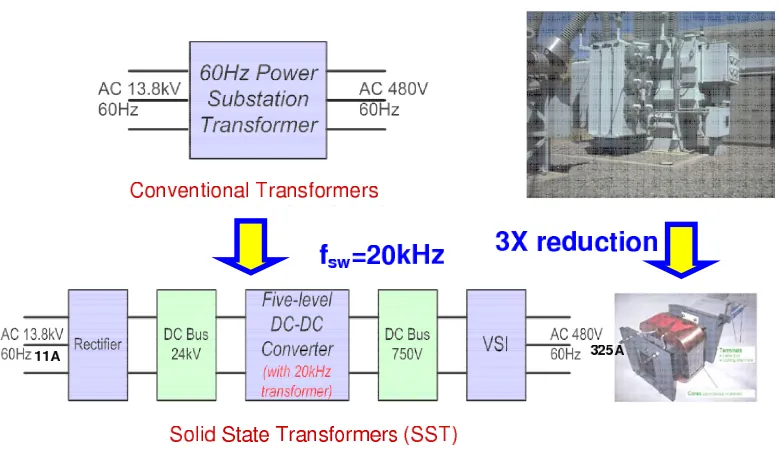
devices in power electronic systems can greatly reduce their size and weight. Our
prelimi-nary study [3] showed that the high-frequency (20 kHz) operation of a 10-kV SiC MOSFETs
based five-level DC/DC converter in a solid-state transformer (SST) can make the weight
and size of the SST three times smaller than that of a conventional 60 Hz mechanical
transformer, as shown in Fig.1.4.
Also, the implementation of high voltage (≥10 kV) power devices in power elec-tronic systems can greatly reduce the part number of series connected switching devices,
Figure 1.3: Power and frequency capabilities of today’s silicon power devices
power devices are not able to meet these stringent requirements even with costly cooling
systems, large numbers of devices in series or parallel connection, and costly snubbers.
Therefore, these applications and situations motivate the development of post-silicon power
devices to achieve high temperature, high voltage and high switching frequency operation
capability.
Wide-bandgap SiC material is the most promising of the post-silicon alternatives because of
its superior properties (e.g., about ten times higher breakdown electric field, higher thermal
conductivity and much lower intrinsic carrier concentration than those of Si). These
su-perior properties enable SiC power devices to operate at high temperatures, high voltages
and high switching frequencies, satisfying the stringent requirements of advanced power
Figure 1.4: Comparison of 10 kV SiC MOSFETs based solid state transformer to conven-tional transformer
1.2
Physical and electrical properties of SiC
Silicon carbide (SiC) is one of the oldest compound semiconductors in the world.
SiC exists in so-called polytypes, which are different crystal structures with the same
sto-ichiometry of a compound semiconductor. Over 250 SiC polytypes have been proven to
exist. The basic unit of structure for all polytypes is a covalently bonded tetrahedron of C
atoms with a Si atom at its center or vice versa, as illustrated in Fig.1.5. The bond length
between Si and C atoms is 1.89 ˚Aand the length between Si-Si or C-C atoms is
approxi-mately 3.08 ˚A.
SiC polytypes are differentiated by the stacking sequence of the tetrahedrally bonded Si-C
bilayers; the individual bond lengths and local atomic environments are nearly identical and
the overall symmetry of the crystal is determined by the stacking periodicity. The most
Figure 1.5: The basic structural unit in SiC, the tetragonal bonding of a carbon atom with four nearest silicon neighbors [5]
structure from the side, the stacking sequence can be shown as in Fig.1.6 [5]. The height
of the unit cell, c, varies with the different polytypes hence the ratio c/a also differs from
one polytype to another polytype. The measuredc/a ratios are approximately 1.641, 3.271
and 4.908 for the 3C-, 4H- and 6H-SiC polytypes, respectively [5].
Out of all of the polytypes of SiC, only 4H-SiC and 6H-SiC are commercially available. At
present, commercial 4H-SiC and 6H-SiC wafers are available at diameters up to 100mm
for research and development samples from a number of manufacturers [6]. The micropipe
densities are as low as 0.8 cm2over an entire 100 mm diameter 4H-SiC wafer. 4H-SiC shows
even more potential for use in high power devices than 6H-SiC because of its higher carrier
mobility and its lower dopant ionization energy. Hence, the power devices to be investigated
in this thesis are based on 4H-SiC.
semicon-Figure 1.6: Stacking orders along c-axis for 3C-, 4H-, and 6H-SiC. Open and closed circles represent Si and C atoms, respectively [5]
ductor applications. A comparison of some properties of SiC and Si is shown in Table 1.1. It
shows that, when compared to silicon, wide bandgap SiC offer a much lower intrinsic carrier
concentration (18 orders of magnitude smaller), a higher electric breakdown field (about 10
times higher), a higher thermal conductivity, and a larger saturated electron drift velocity
(2 times larger).
As shown in Table 1.1, 4H-SiC has a wide bandgap of 3.26 eV at room
tempera-ture. Due to having a wide bandgap, its intrinsic carrier density is very low. For example,
assuming a doping concentration of 2×1014 cm−3, the intrinsic temperature, at which the intrinsic carrier concentration reaches 2×1014 cm−3, is approximately 1100 oC for 4H-SiC, as compared to 245oC for Si. This makes SiC extremely attractive for high-temperature
ap-plications, which also is helpful to reduce the cooling cost and complexity of power electronic
Table 1.1: Comparison of electrical properties of SiC and Si
Material Property Symbol Si SiC Unit
Bandgap Eg 1.1 3.26 eV
Intrinsic Carrier Density ni 1.5×10¹⁰ 8.2×10⁻⁹ cm−3
Critical Electric Field Ec 0.3 3 MV/cm
Electron Mobility µe 1450 900 cm2/Vs
Electron Saturation Velocity vsat 0.86 2 107cm/s
Thermal Conductivity κ 1.5 5 W/cmK
Permittivity ǫ 11.7 9.7
hybrid-electric vehicle’s hood for example, could save space, weight, and cost. Therefore,
SiC technology makes it possible to use the engine’s cooling system and a small heatsink
to cool the power electronics in a hybrid vehicle, making the expense of a dedicated
cool-ing circuit unnecessary. In addition, the large Si-C bondcool-ing energy makes SiC resistant to
chemical attack and radiation, and ensures its stability at high temperatures, which makes
SiC power devices attractive in aerospace applications with reduced radiation shielding.
4H-SiC has a high critical electric field of about 3 MV/cm [7], which is about
10 times higher than that of Si. As a result, a thinner drift layer with a higher doping
concentration can be used for SiC power devices than Si devices at the same blocking
voltage. Thus a low specific on-resistance can be achieved in SiC unipolar devices. Also, a
smaller chip size in SiC unipolar devices can be used to achieve the same forward voltage a
capacitance, fast switching speed and large maximum operation frequency. In addition,
both the storage of minority carriers and associated switching losses of SiC bipolar devices
are smaller than Si bipolar devices. This means the maximum switching frequency of SiC
bipolar devices is larger than that of Si bipolar devices.
4H-SiC has a high saturated drift velocity. The electron saturated drift velocity
of 4H-SiC is as high as 2×107 cm/s, which is twice the saturated drift velocity of Si [8]. During the turn-off transient, when the depletion region forms and expands, minor carriers
are swept out of the depletion region at the saturated drift velocity. Therefore, a higher
saturated drift velocity of 4H-SiC can enable SiC bipolar devices to have a faster switching
speed than Si devices that have the same carrier lifetime in the drift layer.
Another important physical property of SiC is its high thermal conductivity. The
thermal conductivity of 4H-SiC (4.9 K) is more than 3 times that of Si (1.5
W/cm-K). High thermal conductivity reduces thermal impedance of the device packages, allowing
heat generated in SiC-based devices to be more easily transmitted to the ambient. The high
thermal conductivity coupled with the wide bandgap makes SiC power devices suitable for
high temperature switching applications [9] [7], where their junction temperature is more
than twice the junction temperature limit (175oC) of silicon power devices.
To evaluate the performance of semiconductor materials, their unipolar
figures-of-merit (FOM) have also been compared. In 1965, Johnson [10] derived a figure of figures-of-merit,
JFOM =EC·vs/(2π), which assumes the device performance of a typical discrete transistor is
mainly limited by the product of the critical breakdown fieldEC and the electron saturation
velocity vsat. In 1982, Baliga [11] proposed a figure of merit, BFOM = ǫµ·EC3, which
Table 1.2: Comparison of the normalized figures of merits of SiC and Si
figure of merits Si SiC
JFOM 1 540
BFOM 1 515
HMFOM 1 7.5
conduction losses in high-voltage power devices. BFOM is valid only for systems operating
at low frequencies where the conduction losses are dominant. For high frequency switching
applications, In 1989, Baliga proposed another figure of merit, BHFFOM = 1/(Rsp,on·Cin,sp)
[12], which considers the switching losses due to charging and discharging of the device’s
input capacitance. In 2004, Dr. Alex Q. Huang proposed a new material figure of merit
(HMFOM), which considers the swiching losses properly derived from gate charge and
conduction loss [13]. The term (Ecõ) is defined as the new material figure-of-merit called
HMFOM.
Table 1.2 shows the figures-of-merits of SiC and Si. It shows that SiC power
devices can offer great improvements in performance over silicon power devices.
1.3
Challenges of research
With the availability of SiC single crystal wafers from the early 90’s, a number
of government programs are supporting the development of low defect thick epitaxial SiC
materials and high voltage SiC devices. In 2003, the world’s first 10-kV 4H-SiC power
has been made in the development of prototype SiC power devices, the development of high
voltage (≥10kV class) SiC devices is still in its early stages and several important aspects of them have not been investigated extensively.
First, the optimization of high voltage SiC device design should be carried out
to achieve optimum performance trade-off in the early stage of their development. These
optimized design parameters include the devices’ geometry, doping density, mobility, carrier
lifetime, etc.
Second, the choice of device type amongst the SiC power device candidates is
uncertain for more than 10-kV level voltage rating in switching applications. SiC
MOS-FETs, IGBTs and thyristors are possible candidates and the comparison of them needs
to be investigated in order to define their optimum voltage operation range and frequency
capability.
Third, to fully utilize the advantages of high voltage SiC devices in power electronic
systems, the loss extraction, frequency capability and SPICE modeling of SiC power devices
are to be investigated extensively for circuit and system design. Also, their application
prospects and feasibilities in various power electronic systems will be discussed.
1.4
Outline of dissertation
In this dissertation, the design, characterization, SPICE modeling and analysis of
high voltage SiC power devices are investigated extensively. These high voltage SiC power
devices include SiC MOSFET, p-channel IGBT and emitter turn-off thyristors (ETO). The
dissertation consists of eight chapters.
re-search of high voltage SiC power devices.
Chapter 2 extensively investigates the theoretical limits of SiC power devices,
including the theoretical specific on-resistance and frequency capability of SiC unipolar
devices, and the on-set of dynamic avalanche breakdown of SiC bipolar devices. The study
of theoretical specific on-resistance of SiC unipolar devices shows the needed drift layer
thickness of SiC devices is about 10 times smaller than that of Si devices for the same voltage
rating and the theoretical specific on-resistance of SiC unipolar devices is more than 600
times smaller than that of Si devices. Based the theory of HMFOM, the theoretical study of
the frequency capability of SiC and Si unipolar devices shows that SiC unipolar devices can
achieve about 55 time larger operational frequency than Si devices. The theoretical study of
dynamic avalanche of bipolar devices shows that SiC bipolar devices can achieve more than
20 times larger onset power density of dynamic avalanche than Si bipolar devices. These
advantages make SiC devices attractive for applications in high voltage and high frequency
power electronic systems.
At present, power MOSFETs, which are popular in silicon technology, receive
the most attention because of its MOS gate control and inherent fast switching capability
due to their majority carrier conduction mechanism. Therefore, 10-kV SiC MOSFETs are
studied first. Chapter 3 discusses the characterization, modeling and analysis of 10-kV SiC
MOSFETs. The loss information of a 10-kV SiC MOSFET is extracted by experimental
characterization and then a valid SPICE model of a 10-kV SiC MOSFET is built. Using
the built SPICE MOSFET model, a 4-kW boost converter based on a 10-kV SiC MOSFET
is designed and built. The frequency capability of the 10-kV SiC MOSFET is demonstrated
shown in the characterization study and the experiment of the SiC based boost converter
demonstrate their potential in high voltage high frequency power electronic systems.
However, the on-resistance of SiC MOSFETs increases rapidly with junction
tem-perature and blocking voltage. It makes the conduction loss unacceptable for applications
where high DC supply voltages (≥ 10kV) and high temperature operation are used. This stimulates the development of SiC bipolar devices (IGBT and thyristors) to reduce the
con-duction loss due to the strong conductivity modulation in their thick drift layers, especially
at elevated temperatures.
Chapter 4 discusses the design, optimization, characterization and analysis of a
10-kV SiC p-channel IGBT. A 4H-SiC p-IGBT with a novel current enhancement layer (CEL)
structure is fabricated and reported with improved conduction characteristics. The device
exhibited a differential on-resistance of 26 mΩ·cm2 at room temperature. The SiC p-IGBT under clamped inductive load switching conditions with a DC-link voltage of 4 kV and a
load current density of 150 A/cm2 shows a turn-off time of about 1 µs. The approaches to achieve a better performance trade-off between forward voltage drop and turn-off energy
loss are highlighted.
Among the high-voltage SiC devices under development, SiC thyristors are most
promising switching devices for high voltage power systems because of their high voltage
blocking capability and low conduction loss. Chapter 5 discusses the design, fabrication,
characterization and optimization of high voltage SiC emitter turn-off thyristors (ETO). The
experimental demonstration of the world’s first 4.5-kV SiC ETO prototype shows a four
times higher frequency capability than 4.5-kV-class Si counterparts. Numerical simulations
of the high voltage (10-kV) SiC ETO. The results show that the 10-kV SiC n-type ETO
has a much better performance trade-off than that of the p-type ETO due to a smaller
current gain of the lower bipolar transistor. Further improvement of the 10-kV SiC n-type
ETO can be made with adopting an optimum design of the drift layer carrier lifetime and
the buffer layer of the 10-kV SiC GTO. The theoretical analysis and numerical simulation
shows the SiC ETO also has the excellent reverse bias safe operating area (RBSOA).
Chapter 6 compares the losses and frequency capability of 10-kV SiC MOSFET,
IGBT and ETO. Their maximum switching frequency in a 20kVA SST was compared, and
the variation of their maximum switching frequency on active chip size was investigated.
Chapter 7 is a summary of the major contribution of this research work and future
Chapter 2
Theoretical Capability of SiC
Power Devices
2.1
Introduction
Due to the early stage of development of high voltage SiC power devices, many
of the theoretical limits of SiC power devices are not available or have not been studied
extensively. This situation limits the prediction of their application prospects in high voltage
power electronic systems. In this chapter, several theoretical limits of SiC power devices are
studied extensively, including the theoretical specific on-resistance and frequency capability
of SiC unipolar devices, and dynamic avalanche breakdown of SiC bipolar devices.
2.2
Theoretical specific on-resistance of SiC unipolar devices
Avalanche breakdown due to impact ionization in semiconductors will occur when
critical electric field (Ec) of semiconductors. The dependence of the critical electric field in
4H-SiC on doping concentration has been given as follows [7]:
Ec=
2.49×10⁶
1−14log10(1016NcmD−3)
(V /cm) (2.1)
whereND is the doping concentration of 4H-SiC layer. The critical electric field of 4H-SiC
is 3 MV/cm at a doping concentration of 5×1016cm−3, which is about 10 times higher than that in Si.
For power device with an n-type lightly doped drift layer, the blocking junction
can be approximated with a one-side abrupt P+/N junction. The maximum electric field
in the depletion region is given by:
Emax=
r
2qNDVa
ǫs
(2.2)
where Va is the reverse bias voltage, ND is the drift layer doping concentration andǫs is
the dielectric constant of 4H-SiC.
From Eq. (2.2), it can be seen that the maximum electric field in the
deple-tion region increases with increasing bias voltage. When the maximum electric field in
the depletion region of non-punch-through structure SiC power devices reaches the critical
electric field of 4H-SiC, the avalanche breakdown occurs. The breakdown voltage (VB) of
non-punch-through structure 4H-SiC power devices can be derived from equation (2.1) and
(2.2):
VB =
ǫsEc2
2qND
(2.3)
Therefore, for the non-punch-through structure, the doping level (ND) required to
support a given breakdown voltage (VB) can be determined from Eq. (2.3):
ND =
ǫsEc2
2qVB
The required drift layer thickness to sustain the blocking voltage (VB) should be
no less than the maximum depletion width at avalanche breakdown, which is given by:
WD =
s 2ǫsVB
qND
= 2VB
Ec
(2.5)
Thus, the theoretical specific on-resistance (Rsp,on) of 4H-SiC non-punch-through
structure unipolar devices is expressed as:
Rsp,on=
WD
qNDµn
= 4V
2
B
ǫsµnEc3
(2.6)
whereµnis the electron mobility in the drift layer. It is a function of doping concentration
and temperature, as given by [15]:
µn=
950×(300T )−2.8
1 + ( ND 2×10¹⁷)0.76
(2.7)
For Si, the drift layer thickness required to support a given blocking voltage is
given by [16]:
WD = 2.58×10⁻⁶V
7 6
B (2.8)
Based on Eq. (2.5) and (2.8), the required drift layer thickness as a function of
blocking voltage for SiC and Si non-punch-through unipolar devices is plotted and shown
in Fig.2.1. It shows the drift layer thickness of non-punch-through SiC power devices is
approximately 10 times smaller than that of Si devices at the same blocking voltage. Thus,
SiC bipolar devices have less stored charge and faster switching speed than Si bipolar devices
at the same carrier lifetime and forward current density. This makes 4H-SiC bipolar devices
attractive for high voltage and high frequency power electronics applications.
The theoretical specific on-resistance of Si unipolar device at room temperature is
given by [16]:
1 10 10
1 10
2 10
3
S iC
S i
W
D
(
m
)
Blocking Voltage (kV)
Figure 2.1: Comparison of drift layer thickness of Si and SiC power devices as a function of blocking voltage
The theoretical specific on-resistance of Si and 4H-SiC unipolar devices at room temperature
is plotted in Fig.2.2. It can be seen that the specific on-resistance of SiC unipolar devices
can be about 600 times lower than that of Si devices for 1 kV voltage rating due to the
higher critical electric field of SiC.
2.3
Theoretical frequency capability of SiC unipolar devices
SiC power devices are very attractive for high frequency switching applications.
This is of interest in the application of DC-DC power converters, where an increase in
switch-ing frequency corresponds to a decrease in size and weight, as well as an increase in power
1 10 10 -1 10 0 10 1 10 2 10 3 10 4 10 5 S iC S i R o n , s p ( m . c m 2 )
Blocking Voltage (kV)
Figure 2.2: Comparison of theoretical specific on-resistance of Si and SiC unipolar devices at room temperature
2.3.1 Brief introduction of HMFOM
Several device or material figures of merit have been published in the literature,
including JFOM, BFOM and BHFFOM. These figures of merit can not be directly used to
compare the switching loss of unipolar power devices based on various materials, therefore,
Dr. Alex Q. Huang proposed a new material figure of merit (HMFOM) in 2004, which
considers the swiching losses properly derived from gate charge and conduction loss [13].
The switching waveforms of a unipolar power device can be best described by the
gate-charge curve. Switching loss of all unipolar power devices (JFET, MOSFET, MESFET,
etc.) can more accurately be estimated based on the gate charge waveform.
Assuming the turn-on loss is equal to turn-off loss, the loss of unipolar devices in
converters is expressed as
Ploss ≈Irms2 Ron+VDIDtff =
Irms2 Ron,sp
A +
VDIDf Qgd,spA
ig,av
where the first term stands for the conduction loss, the second term stands for the switching
loss, VD is the DC-link voltage in the converter, Irms is the rms current of the converter,
ID is the load current of the converter, tf is the voltage rise time of the device, f is the
switching frequency, A is the area of the device,Ron,sp is the specific on-resistance, Qgd,sp
is the specific gate-drain charge andig,av is the average gate drive current.
As the area of the device increases, the first term decreases and the second term
increases. Consequently, the power loss exhibits a minimum value when dPloss/dA=0.
Therefore, the minimum loss of the device is expressed as
Ploss,min= 2Irms
s
VDIDf
ig,av
Ron,spQgd,sp (2.11)
To compare the relative advantages of unipolar devices based on different
mate-rials, it would be advantageous to relate the FOM to material properties. If the device is
fabricated on a uniformly doped semiconductor layer with a doping of ND, and an abrupt
junction is assumed, the theoretical specific on-resistance of unipolar devices is given by Eq.
(2.6).
The gate charge of a unipolar device, Qgd, is the integration of the gate-to-drain
capacitance over the change from a DC-link voltageVDto the device’s forward voltage drop
(a very small value), is predominantly determined by the charge of the drain’s depletion
layer underneath the gate when the device is supporting the DC-link voltage. Therefore,
from Gauss’s law, we obtain an expression for Qgd,sp.
Qgd,sp=kεED =k
r
VD
VB
εEc (2.12)
where ED is the peak electric field when V=VD, and ε is the dielectric constant of the
to the whole chip area, and it is typically determined by processing capability rather than
material properties.
From Eq. (2.6) and Eq. (2.12), one obtains
Rgd,spQgd,sp=
4kVB√VBVD
µE2
c
(2.13)
Substituting Eq. (2.13) into Eq. (2.11), we can get
Ploss,min=
4√DI 3 2
D(VBVD)
3 4
q
kiDf
ig,av Ecõ
(2.14)
whereVB is the blocking voltage of the device.
The term (Ecõ) is defined as the new material figure-of-merit called HMFOM,
HM F OM =Ecõ (2.15)
2.3.2 Theoretical frequency capability
For very high voltage SiC unipolar devices in power conversion applications, the
device’s turn-on losses usually are larger than the turn-off losses due to the reverse recovery
of the freewheeling diode [17]. The assumption of equal turn-on and turn-off losses in the
derivation of HMFOM should be modified accordingly. Assuming the ratio of the turn-on
loss to the turn-off loss is ζ (≥1) in a high voltage SiC unipolar device, the total loss of a unipolar device in a converter consists of conduction, turn-on loss and turn-off loss and is
expressed as
Ploss =Irms2 Ron+
1 +ζ
2 VDIDtff =
I2
rmsRon,sp
A +
1 +ζ
2
VDIDf Qgd,spA
ig,av
(2.16)
Therefore, the minimum loss of the device in a converter is expressed as
Ploss,min= 2Irms
s 1 +ζ
2
VDIDf
ig,av
Substituting Eq. (2.13) into Eq. (2.17), we can get
Ploss,min=
4Irms(VBVD)
3 4
r
k(1+2ζ)IDf
ig,av Ecõ
(2.18)
From Eq. (2.18), the operation frequency of SiC unipolar devices is expressed as
f = P
2
lossE2cig,avµ
16I2
rmsID(VBVD)
3 2k(1+ζ
2 )
(2.19)
wherePlossis the total loss of the power device allowed by thermal management.
Eq. (2.19) shows the maximum operation frequency of unipolar devices is in
proportion to HMFOM2. This means SiC unipolar devices can achieve about 55 times
larger maximum operation frequency than their Si counterparts for the same device voltage
rating and circuit conditions.
Assuming a unipolar power device operates in a converter with a DC-link voltage
that is 50 percent of its blocking voltage (VD=VB/2), a duty cycle of D (Irms=
√ D·ID),
the operation frequency of SiC unipolar devices can be simplified to
f = P
2
lossE2cig,avµ
2.828DID3VB3k(1 +ζ) (2.20)
Eq. (2.20) shows the maximum operation frequency of unipolar devices is inversely
proportional to VB3 and ID3, and proportional toPloss2. Eq. (2.19) also shows the
maxi-mum operation frequency of unipolar devices is proportional to Ploss2. This indicates that
with better thermal management, the power devices can be operated at a higher maximum
frequency.
When 1 cm2 Si and SiC MOSFETs with a geometry factor of 0.5 (k=0.5) and a
A (ig,av), a total power loss of 400 W, and a corresponding junction temperature of 175oC,
the variation of their maximum operation frequency with their blocking voltage is plotted
in Fig.2.3. For a 1 cm2 10-kV SiC unipolar device, its maximum operation frequency is
estimated to be 33 kHz.
2 4 6 8 10 12 14 16 18 20
0 1 10 100 1000 10000 100000
Si theoretical limit
at 175 o
C
SiC theoretical limit at 175 o C M a x i m u m f r e q u e n c y ( k H z )
Blocking Voltage (kV)
Figure 2.3: Calculated frequency capabilities of Si and SiC unipolar devices vs. their blocking voltage at specified conditions
2.4
Theoretical dynamic avalanche breakdown of 4H-SiC
bipo-lar devices
Rapid improvement of 4H-SiC material quality and maturation of SiC device
switching applications. As one of the major concern of bipolar devices, the onset of dynamic
avalanche breakdown of SiC pnp and npn transistors has been systematically analyzed.
Figure 2.4: Schematic illustration of dynamic avalanche of SiC bipolar devices
Dynamic avalanche breakdown (or avalanche injection) is a basic failure mechanism of
bipo-lar devices [18]. Fig.2.4 shows schematic illustration of dynamic avalanche of SiC punch
through structure bipolar devices. When the turn-off process of a SiC n-type bipolar
de-vice is determined by the turn-off of an open base pnp transistor (hard-driven turn-off),
the current transport in the depletion region occurs exclusively via holes. Due to the high
electric field prevalent in the depletion region, holes pass through the depletion region at
the saturated drift velocity (vsat,p). The presence of holes adds charge to the space charge
its turn-off transient, the net charge in the space charge region is given by
Nef f ≈ND+
JA
q·vsat,p
(2.21)
where the first term ND is then− drift layer doping concentration (cm−3), the second term
is the current controlled hole concentration,vsat,p is the hole saturated drift velocity (cm/s)
and its value is about 8.6×106 cm/s for 4H-SiC [19], and JA is the anode current density
(A/cm2).
For high voltage Si bipolar devices, the second term on the right of Eq. (2.21),
the current controlled hole concentration, is much larger than the first term (ND) and the
first term can be neglected at a high current density. However, because the critical electric
field of 4H-SiC is about 10 times larger than that of Si, for the same breakdown voltage,
the doping concentration of the drift region of 4H-SiC power devices is 10 times larger than
that of Si power devices and is a large component of the net charge compared to the current
controlled hole concentration at a high current density.
The electric field distribution in the depletion region is determined by the net
charge (Nef f). Poisson’s equation in the space charge region is expressed as
dE(x)
dx =− q εs
Nef f ≈ −
q εs
(ND + JA
q·vsat,p
) (2.22)
The presence of holes in the space charge region increases the slope of the electric
field profile and the peak electric field at the p-base/n− drift region junction. When the
peak electric field reaches a critical value (EC), the onset of dynamic avalanche breakdown
occurs. An empirical relation may be established for the dependence of the critical electric
field on the effective carrier concentration in 4H-SiC, and is given in Eq. (2.1).
According to Poisson’s equation, the onset of dynamic avalanche breakdown of SiC
current density is higher than a specific current density (Jth) given by
Jth=q.vsat,p·(
εs·Ec
q·Wpt −
ND) (2.23)
where Wpt is the drift layer thickness of a punch through structure SiC n-type bipolar
device.
For a designed 10-kV SiC n-type punch through GTO with a 100µm thick, 6×1014 cm−3doped drift layer, a current density of Jth=400 A/cm2 is required to form a triangular
electric field profile at the onset of dynamic avalanche breakdown. When the load current is
below theJth(JA≤Jth), the electric field in the drift layer has a trapezoidal profile. Ignoring
the effect of the bipolar transistor current gain on the breakdown voltage of SiC bipolar
devices because of a small gain in a punch through structure device, the onset voltage of
dynamic avalanche breakdown of a SiC n-type bipolar device is simply expressed as that of
a parallel-plane abrupt junction diode, as given by
BVdy ≈EC·Wpt− q·Nef f·W
2 pt 2·εs
= 2.49×10⁶
1−1 4log10(
ND+ JA q.vsat,p 1016 )
·Wpt−9.42×10⁻⁸·(ND +q·vJsat,pA )·Wpt2
(2.24)
When JA>Jth, the onset voltage of dynamic avalanche of a SiC n-type bipolar
device is expressed as
BVdy ≈12EC·Wpt=
εsEC(Nef f)2 2qNef f
= εs
2q(ND+q·vsat,pJA )
·( 2.49×10⁶
1−1 4log10(
ND+ JA q.vsat,p 1016 )
)2 (2.25)
Similarly, the onset voltage of dynamic avalanche of a Si n-type bipolar device is
expressed as
BVdy≈
1
2EC ·W =
5.34×10¹³ (ND+q·vJsat,pA )
3 4
0 2 4 6 8 10 12 14 0
200 400 600 800 1000
A
B
10-kV SiC n type bipolar device
dynamic avalanche
10-kV Si n type bipolar device On-set of dynamic avalanche
J
C
(
A
/
c
m
2
)
V C
(kV)
Figure 2.5: Current density vs. onset voltage of dynamic avalanche breakdown of the 10-kV SiC and Si n-type bipolar devices
The curves A and B in Fig.2.5 shows the theoretical onset of dynamic avalanche breakdown
of 10-kV SiC and Si n-type bipolar devices under the hard-driven switching condition, as
predicted by Eq. (2.24) (2.24) (2.26). It shows that the onset power density of dynamic
avalanche of the 10-kV SiC bipolar device is more than 7 MW/cm2, while the onset power
density of dynamic avalanche of the 10-kV Si bipolar device is about 250 kW/cm2.
There-fore, SiC bipolar devices have much better ruggedness than Si bipolar power devices.
In 4H-SiC, the impact ionization coefficient of holes is much larger than that
of electrons. This is related to the energy band structure of 4H-SiC and can be mainly
explained by the discontinuous conduction band suppressing the electron heating and impact
acceptor doping concentration can be approximated by a relationship [20].
EC = 3.3×10⁴·Nef f1/8 (2.27)
Similar to Eq. (2.23), when the cathode current density is less than a specific
current density
|JC|<|Jth| (2.28)
The onset voltage of dynamic avalanche of a 4H SiC p-type bipolar device is
expressed as
BVdy= [3.3×10⁴·(NA+ |
JC|
q·vsat,n
)18 ·W
pt−9.42×10⁻⁸·(NA+ |
JC|
q·vsat,n
)·Wpt2] (2.29)
when the cathode current density is larger than a specific current density
|JC|>|Jth| (2.30)
the onset voltage of dynamic avalanche of a 4H SiC p-type bipolar device is expressed as
BVdy =
2.9×10¹⁵ (NA+q·|vJsat,nC| )
3 4
(2.31)
The hole saturated drift velocity (vsat,p≈0.86×107 cm/s) of 4H-SiC is smaller than
the electron saturated drift velocity (vsat,n≈1.83×107 cm/s) [8], so the effective carrier
density in the space charge region of a pnp transistor is larger than that of a npn transistor
during the turn-off transient at the same load current density. Therefore, SiC pnp transistors
have a smaller onset voltage of dynamic avalanche than npn transistors due to the larger
saturated drift velocity and smaller impact ionization coefficient of electron in 4H-SiC than
those of holes. Calculated from Eqs.(2.24), (2.25), (2.29), and (2.31), the onset of dynamic
turn-off condition is shown in Fig.2.6. The onset dynamic avalanche breakdown of the
10-kV SiC p-type bipolar device is nearly as large as its static breakdown voltage.
0 2 4 6 8 10 12 14
0 200 400 600 800 1000
10-kV p type bipolar device
10-kV n type bipolar device
I
J
C
I
(
A
/
c
m
2
)
IV
C
I (kV)
Figure 2.6: Current density vs. onset voltage of dynamic avalanche breakdown of 10-kV SiC n-type and p-type bipolar device
2.5
Summary
In this chapter, several theoretical limits of SiC and Si power devices are
stud-ied extensively, including the theoretical specific on-resistance and frequency capability of
unipolar devices and dynamic avalanche breakdown voltage of bipolar devices. The study
of theoretical specific on-resistance shows the needed drift layer thickness of SiC unipolar
devices is about 10 times smaller than that of Si devices for the same voltage rating and
the theoretical specific on-resistance of high voltage SiC unipolar devices is more than 600
capability of SiC and Si unipolar devices shows that SiC unipolar devices can achieve about
55 times larger operation frequency than Si devices. The study of dynamic avalanche of
bipolar devices shows that SiC bipolar devices can achieve more than 20 time larger power
density at the onset of dynamic avalanche than Si bipolar devices. These advantages make
SiC devices attractive for applications in high voltage and high frequency power electronic
Chapter 3
Characterization, SPICE Modeling
and Analysis of 10-kV 4H-SiC
MOSFET
3.1
Introduction of power MOSFETs
Power MOSFETs, also termed vertical geometry co-planer double-diffused
MOS-FET (DMOSMOS-FETs) were developed in 1970’s. They have several advantages, which make
them suitable for many applications. First, power MOSFETs greatly simplify the driver
circuit and reduce the total cost of power electronic systems due to its high input impedance
gate structure. Second, power MOSFETs have fast switching speed due to their inherent
majority carrier conduction mechanism. Third, power MOSFETs also have an excellent
safe operating area: they can withstand the simultaneous application of high current and
power MOSFETs are widely used today in many low voltage applications.
There are various structures of power MOSFETs that have been developed in
market, such as the trench MOSFETs, HEXFETs, and CoolMOS [21][22]. For the purpose
of basic introduction of power MOSFETs, this work focuses on the basic vertical diffusion
power MOSFET cross section. Fig.3.1 shows the cross section of a basic n-channel power
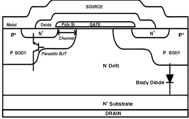
MOSFET cell structure. The device is fabricated on a wafer with an N− drift region epitaxially grown on top of an N+substrate. The P body region and the N+source contact
regions are created using a diffusion process through a common window defined by the edge
of the polysilicon gate. The P body region is driven in deeper than the N+ source contact
region, and the difference in the lateral diffusion between the P body and N+source contact
region defines the surface channel region.
3.1.1 Operation principal
There are three primary modes of operation for the power MOSFET: the linear
region, the saturation region and the forward blocking, as illustrated in Fig.3.2.
L i n e a r r e g i o n
Saturation region
I
D
V
GS
=0 V
GS
> V
th
V
DS
Figure 3.2: Output characteristic of a basic Si n-channel power MOSFET cell structure
When the gate is short-circuited to the source, the device can support a large
drain voltage across the P-body/N− drift layer junction. The forward blocking capability is shown in the Fig.3.2 by the lowest curve. The forward breakdown voltage is determined
by the avalanche breakdown voltage of the P-base/N− drift layer junction.
When the gate-source voltage exceeds the threshold (VGS≥VT h), an inversion layer
forms beneath the gate oxide of the power MOSFET and the channel becomes conductive,
on-resistance. The on-resistance determines the power dissipation during current condition and
is mainly governed by the sum of the channel resistance, JFET resistance and drift region
resistance. At large drain voltages, the resistance of the power MOSFET increases due to
pinch off of the JFET region. Ultimately, the current saturates at high drain voltages.
3.1.2 Internal capacitances
There are several internal capacitances associated with the power MOSFET as
shown in Fig.3.3. The gate-source capacitance (CGS) is the capacitance due to the overlap
of the source and the channel regions by the polysilicon gate and is independent of drain
voltage. The gate-drain capacitance (CGD) is the capacitance associated with the overlap of
the polysilicon gate and the silicon underneath. CGD is a nonlinear function of drain voltage.
The drain-source capacitance (CDS), associated with the body diode, varies inversely with
the square root of the drain-source voltage.
The equivalent circuit of a power MOSFET is shown in Fig.3.4, which includes
the intrinsic diode and internal capacitances. The capacitances of a power MOSFET are
shown in Fig.3.4, play a significant role on the shape of its voltage and current switching
waveforms by governing the rate at which the gate driver charges/discharges CGS and
CGD. Therefore, these capacitances largely dictate the switching speed and switching loss
of a power MOSFET, and the efficiency of its gate driver circuit.
Figure 3.4: Equivalent circuit of a MOSFET
3.1.3 Switching performance
The switching performance of a power MOSFET is analyzed in a clamped inductive
load circuit, as shown in Fig.3.5. The circuit is a fundamental circuit widely used in a
step down DC/DC converter; the following switching analysis of a power MOSFET is
switching performance of a power MOSFET, several assumptions are made, including (1)
the freewheeling diode is an ideal diode; (2) stray inductance is not taken into account; (3)
the load current flowing through the inductor is constant.
Figure 3.5: Circuit used for transient analysis of a power MOSFET
The turn-on transient waveforms of a power MOSFET in the clamped inductive
load circuit is shown in Fig.3.6. There are several important time intervals of the turn-on
transient of a power MOSFET. The equivalent circuits of the inductive load circuit of a
power MOSFET in the corresponding time intervals are shown in Fig.3.7.
After applying a pulse signal to the gate to turn the device on, the gate voltage of a power
MOSFET, VGS, increases from zero to its threshold voltage (VT) and its drain current is
kept at almost zero in the time interval ta. The equivalent circuit during the time interval
![Figure 1.1: Applications of silicon power devices [1]](https://thumb-us.123doks.com/thumbv2/123dok_us/1330164.1165977/20.612.228.414.169.410/figure-applications-of-silicon-power-devices.webp)
![Figure 1.2: Power range of commercially available high power semiconductor devices [2]](https://thumb-us.123doks.com/thumbv2/123dok_us/1330164.1165977/21.612.151.497.107.345/figure-power-range-commercially-available-power-semiconductor-devices.webp)
![Figure 1.5: The basic structural unit in SiC, the tetragonal bonding of a carbon atom withfour nearest silicon neighbors [5]](https://thumb-us.123doks.com/thumbv2/123dok_us/1330164.1165977/24.612.174.471.111.332/figure-structural-tetragonal-bonding-withfour-nearest-silicon-neighbors.webp)
![Figure 1.6: Stacking orders along c-axis for 3C-, 4H-, and 6H-SiC. Open and closed circlesrepresent Si and C atoms, respectively [5]](https://thumb-us.123doks.com/thumbv2/123dok_us/1330164.1165977/25.612.158.492.113.329/figure-stacking-orders-open-closed-circlesrepresent-atoms-respectively.webp)