ABSTRACT
WANG, GANGYAO. Design, Development and Control of >13 kV Silicon-Carbide MOSFET based Solid State Transformer (SST). (Under the direction of Dr. Alex Huang.)
Within the advent of the smart grid system, the solid state transformer (SST) will
replace the traditional 60 Hz transformer formed by silicon steel core and copper
windings and provides the interface between the high distribution voltage and low
utility voltage. Other than the smaller size and less weight, SST also brings many
more functionalities including voltage regulation, reactive power compensation, power
management and renewable energy integration. The motivation of this research is to
design a solid state transformer based on the wide band-gap Silicon Carbide (SiC)
power MOSFETs and compare it with the silicon IGBT based SST.
With wider band-gap and higher critical electrical field, the high voltage SiC power
device has advantages over silicon power device for both conduction and switching.
An extensive study and characterization of the SiC MOSFET was first carried out.
It has been found that the MOSFET parasitic capacitors store significant amount of
energy and the MOSFET turn on loss is high but turn off loss is virtually zero with
small enough turn on gate resistor. A method for estimating the MOSFET parasitic
capacitances has been proposed and explained in detail. A PLECS loss simulation
model has been developed for the >13 kV SiC MOSFET which has been verified
through a boost converter with the SiC MOSFET switches under 40 kHz for both soft
switching and hard switching conditions separately.
Widely used full bridge circuit has been chosen as the topology for the SST rectifier
for its simple structure and bidirectional power transfer capability. Form three different
identified as the most suitable control algorithm for the >13 kV SiC MOSFET base
rectifier. With such modulation method, the generated PWM voltage frequency equals
to the switching frequency, the each MOSFET equivalent switching frequency under
hard switching conditions is only 1/4 of the PWM voltage frequency. The SST rectifier
efficiency has been simulated and measured for 6 kHz and 12 kHz switching frequency
with 6 kV dc bus voltage and 3.6 kV ac voltage, which is 99.2% for 6 kHz with 8.8 kW
load and 98.5% for 12 kHz with 8.3 kW load.
The SST DC-DC stage utilize the dual active half bridge (DHB) as the topology, its
zero voltage switching (ZVS) turn on range has been analyzed and it is concluded
that the dead-time and device parasitic capacitances will reduce the ZVS range while
the magnetizing current will increase the ZVS range. Since the SiC MOSFET has
very high turn on loss, it is desired to have ZVS for the full load range. The high
frequency transformer with integrated leakage inductance for the DHB operation has
been designed, the magnetizing inductance has been decreased for increasing the ZVS
range. The DC-DC stage efficiency has been measured as 96.9% for 10 kHz switching
frequency and 10 kW load, and the peak efficiency is 97.5% for 10 kHz switching
frequency and 5 kW load.
The SST inverter stage is similar to many other PV inverters or motor drives. The
research in this thesis is focus on characterizing the newly released 1200 V 100 A SiC
MOSFET, evaluating its performance and comparing it with the same rating Si IGBT.
It has been found that the SiC MOSFET based inverter efficiency will increase from
98% to 99% for 20 kHz switching frequency, and from 96.5% to 98.5% for 40 kHz
switching frequency.
In summary, both the >13 kV and 1200 V SiC MOSFET has been fully characterized
© Copyright 2013 by Gangyao Wang
Design, Development and Control of >13 kV Silicon-Carbide MOSFET based Solid State Transformer (SST)
by
Gangyao Wang
A dissertation submitted to the Graduate Faculty of North Carolina State University
in partial fulfillment of the requirements for the Degree of
Doctor of Philosophy
Electrical Engineering
Raleigh, North Carolina
2013
APPROVED BY:
Dr. Subhashish Bhattacharya Dr. Mesut Baran
Dr. Srdjan Lukic Dr. Alex Huang
DEDICATION
To my parents
Gongcheng Wang and Chengmiao Chu
BIOGRAPHY
Gangyao Wang was born in Yuexi, Anhui province, China. He received his B.S. degree
in electrical engineering from the Nanjing University of Aeronautics and Astronautics,
Nanjing, China, in 2004. From 2005 to 2007, he was an Electrical Engineer with
Delta Electronics Shanghai Design Center, Shanghai, China. Since 2007 he has been
working toward the Ph.D. degree at the Future Renewable Electric Energy Delivery
and Management (FREEDM) Systems Center, Department of Electrical and Computer
Engineering, North Carolina State University, Raleigh. His research interests include
power converter topology and control, solid-state transformer design, SiC power
device characterization, modeling and application.
ACKNOWLEDGEMENTS
I would like to express my deepest gratitude to my advisor, Dr. Alex Huang, for
his guidance, continuous support and encouragement throughout my PhD study. I
have benefited tremendously from his extensive knowledge, broad vision and creative
thinking during my research work. It has been always joyful and inspiring to discuss
various subjects with him. I am grateful to Dr. Subhashish Bhattacharya, Dr. Mesut
Baran, and Dr. Srdjan Lukic for their valuable discussions and guidance about my
research.
I am deeply thankful to the SST(Solid State Transformer) team members including
Dr. Tiefu Zhao, Dr. Xu She, Mr. Fei Wang, Mr. Arun Kadavelugu, Mr Seunghun Baek,
Mr. Sumit Dutta, Mr.Joe Elliott, Dr Xijun Ni, Mr.Yang Lei, Mr. Even Xiong, Mr. Gari
Magai, Dr Chushan Li, Dr. Wenxi Yao, Dr. Wu Chen, Dr.Yang Liu and many others
who have been worked on the SST projects.
It has been a great pleasure to work with so many talented and helpful colleagues
and friends in the SPEC center and FREEDM systems center. I would like to thank
you Dr. Bin Chen, Dr. Yu Liu, Dr. Wenchao Song, Dr. Jinseok Park, Dr. Xiaojun Xu, Dr.
Jiwei Fan, Dr. Liyu Yang, Dr. Xin Zhou, Dr. Sungkeun Lim, Dr. Xiaopeng Wang, Dr.
Jun Wang, Dr. Jeesung Jung, Dr. Parkhideh Babak, Dr. Jun Li, Dr. Xiaohu Zhou, Mr.
Jifeng Qin, Ms. Juming Lai, Dr. Qian Chen, Dr Yu Du, Dr Zhigang Liang, Dr. Woongje
Sung, Dr. Zhengping Xi, Dr. Zhan Shen, Dr. Sanzhong Bai, Mr. Xunwei Yu, Dr. Xiang
Lu, Dr. Edward van Brunt, Mr. Xin Huang, Ms Jing Yao, Mr. Thomas Nudell, Mr.Eric
Green, Mr. Yen-Mo Chen, Mr. Li Jiang, Mr. Zhuoning Liu, Ms. Huan Hu, Mr. Yalin
Wang, Mr. Xingchen Yang, Dr. Pochih Lin, Mr. Kai Tan, Mr. Jiadi Jiang,Ms. Wenbo
Zhang, Ms. Suxuan Guo, Mr. Yizhe Xu, Mr. Rui Wang, Mr. Rui Gao,Mr. Mohammad
Ali Rezaei, Mr. Samir Hazra, Mr Sachin Madhusoodhanan, Mr. Elie Najm, Mr. Anand
Ramamurthy, Mr. Arvind Govindaraj, Mr. Habiballah Rahimi-Eichi, Mr. Hesame
Mirzaee. Mr. Xiaoqing Song, Mr. Fei Xue, Ms. Li Wang, Mr.Chang Peng and etc.
I would also like to thank the FREEDM administrative and lab management
staff, Mr. Hulgize Kassa, Ms Karen Autry, Ms Collen Reid, Mr Rogelio Sulivan, Dr
Ewan Pritchard, Mr Seth Crossno, Ms.Audrey Callahan, Ms. Penny Jeffrey, Ms. Pam
Carpenter, for their countless help during my research.
My heartfelt appreciation goes toward my parents, Gongcheng Wang and
Cheng-miao Chu for their endless love, trust, encouragement and support during my life.
TABLE OF CONTENTS
LIST OF TABLES . . . viii
LIST OF FIGURES . . . ix
Chapter 1 Introduction . . . 1
1.1 Introduction of SST Concept . . . 1
1.2 Silicon IGBT based SST . . . 3
1.3 SiC Power Device based SST . . . 5
1.4 Outline of This Dissertation . . . 7
Chapter 2 Characterization of the High Voltage Power Semiconductor De-vices . . . 9
2.1 Introduction . . . 9
2.2 General Approaches for Power Device Characterization . . . 10
2.2.1 Leakage Current Measurement . . . 10
2.2.2 Dynamic Switching Test . . . 12
2.3 Characterization of 6.5 kV 25 A IGBT . . . 14
2.3.1 Introduction . . . 14
2.3.2 Static Performance . . . 16
2.3.3 Switching Performance . . . 16
2.4 IGBT Gate Driver Design Consideration . . . 20
2.5 Characterization and Modeling of 13 kV 10 A SiC MOSFET . . . 26
2.5.1 Introduction . . . 26
2.5.2 Static Characteristics . . . 27
2.5.3 Switching Transient and Loss analysis . . . 31
2.5.4 MOSFET Parasitic Capacitances Measurement . . . 45
2.5.5 MOSFET Loss Model . . . 51
2.5.6 Experiment Verification . . . 53
2.5.7 High Voltage SiC MOSFET Gate Driver . . . 59
2.5.8 Comparisons of 6.5 kV IGBT and >13 kV SiC MOSFET . . . 60
2.6 Comparisons of High Voltage SiC IGBT and MOSFET . . . 63
2.6.1 Introduction . . . 63
2.6.2 Switching Loss Test Setup . . . 63
2.6.3 Switching Transient under Different Temperature . . . 64
2.6.4 Switching Loss and Frequency Capability . . . 70
Chapter 3 SST Rectifier Stage Design . . . 75
3.1 Introduction . . . 75
3.2 Design of the Rectifier Stage . . . 76
3.2.1 Continuous Current Mode (CCM) Rectifier Control . . . 76
3.2.2 Power Device Loss for the Rectifier . . . 80
3.2.3 Rectifier Filter Design . . . 82
3.3 Experiment Results . . . 88
3.4 Rectifier Loss Simulation for 12 kV DC bus . . . 90
Chapter 4 SST DC-DC Stage Design . . . 92
4.1 Introduction . . . 92
4.2 Dual Active Half Bridge (DHB) ZVS Range Analysis and Extension Method . . . 94
4.3 High Frequency Transformer Design . . . 98
4.4 Simulation Verification of the ZVS Range . . . 100
4.5 Variable Frequency Control and Experiment Results . . . 103
Chapter 5 SST Inverter Stage Design . . . 106
5.1 Introduction . . . 106
5.2 Comprehensive Performance Evaluation of the 1200 V 100 A SiC MOS-FET and Silicon IGBT . . . 108
5.2.1 Forward Characteristics Comparison . . . 108
5.2.2 Switching Characteristics Comparison . . . 110
5.3 Prototype Design, Experiment and Loss Simulation . . . 114
Chapter 6 Conclusions and Future Work . . . 120
References . . . 122
LIST OF TABLES
Table 3.1 Harmonic Limitation for Grid Connected Inverter in IEEE 1547 . 83
Table 4.1 DHB Transformer Design Parameters . . . 100
Table 5.1 MOSFET vs IGBT Switching Loss Comparison Summary . . . 111 Table 5.2 Inverter Stage Test Cases . . . 116
LIST OF FIGURES
Figure 1.1 Role of Solid State Transformer (SST) under FREEDM Systems . 2
Figure 1.2 SST Enabled Energy Internet . . . 3
Figure 1.3 6.5 kV IGBT based Solid State Transformer Topology . . . 4
Figure 1.4 6.5 kV IGBT based Solid State Transformer Prototype . . . 4
Figure 1.5 High Voltage SiC MOSFET based Solid State Transformer Topology 5 Figure 1.6 High Voltage SiC MOSFET based Solid State Transformer Proto-type Front View (a) and Back View (b) . . . 6
Figure 2.1 Circuit for High Voltage Power Device Leakage Current Mea-surement . . . 11
Figure 2.2 Double Pulses Tester . . . 12
Figure 2.3 Double Pulses Test Typical Switching Waveforms . . . 13
Figure 2.4 6.5 kV 25 A IGBT Dual Module Layout . . . 14
Figure 2.5 6.5 kV 25 A IGBT Dual Module Sub-assemblies . . . 15
Figure 2.6 6.5 kV 25 A IGBT Dual Module Prototype . . . 15
Figure 2.7 6.5 kV 25 A IGBT and 6.5 kV 50 A Diode I-V Curve . . . 16
Figure 2.8 6.5 kV 25 A IGBT 3.8 kV 10 A Turn on . . . 17
Figure 2.9 6.5 kV 25 A IGBT 3.8 kV 10 A Turn off . . . 17
Figure 2.10 6.5 kV 25 A IGBT Eon (mJ) under Different Voltages and Currents 18 Figure 2.11 6.5 kV 25 A IGBT Eo f f(mJ) under Different Voltages and Currents 19 Figure 2.12 6.5 kV 25 A IGBT Module Parallel DiodeErec(mJ) under Different Voltages and Currents . . . 19
Figure 2.13 IGBT Switching Test Circuit . . . 20
Figure 2.14 IGBT Turn On Process . . . 21
Figure 2.15 IGBT Turn On (Rg=100 ohm, Le=100 nH, without Zener) . . . 22
Figure 2.16 IGBT Turn On (Rg=100 ohm, Le=100 nH, with Zener) . . . 23
Figure 2.17 IGBT Turn On (Rg=10 ohm, Le=100 nH, with Zener) . . . 24
Figure 2.18 IGBT Turn Off (Rg=10 ohm,dv/dt=3.18 kV/us, Eon=24.5 mJ) . . 25
Figure 2.19 IGBT Turn Off (Rg=220 ohm,dv/dt=3.23 kV/us, Eon=22.6 mJ) . . 25
Figure 2.20 Simplified >13 kV SiC MOSFET Cross Section . . . 26
Figure 2.21 >13 kV SiC 10 A MOSFET Module Schematic and Prototype . . . 27
Figure 2.22 >13 kV SiC 10 A MOSFET Module Leakage Current . . . 28
Figure 2.23 >13 kV SiC 10 A MOSFET V-I Curves . . . 29
Figure 2.24 SiC MOSFET Saturation Current vs Gate Voltage . . . 30
Figure 2.25 >13 kV SiC 10 A JBS Diode I-V Curves for Different Temperature 31 Figure 2.26 Si MOSFET Turn on and Turn off . . . 32
Figure 2.27 MOSFET Turn on Process . . . 34
Figure 2.28 MOSFET Internal Parasitic Capacitance Discharging During Turn
on . . . 35
Figure 2.29 RC Charging Circuit . . . 37
Figure 2.30 SiC MOSFET Turn on for Different Rg . . . 39
Figure 2.31 SiC MOSFET Turn on for Different Rg . . . 39
Figure 2.32 SiC MOSFET Eon . . . 40
Figure 2.33 MOSFET Turn off Process . . . 41
Figure 2.34 MOSFET Internal Parasitic Capacitance Discharging During Turn off . . . 43
Figure 2.35 SiC MOSFET Turn off for Different Rg . . . 44
Figure 2.36 SiC MOSFET Turn off for Different Rg . . . 44
Figure 2.37 SiC MOSFET Turn off Energy for Different Rg . . . 45
Figure 2.38 SiC MOSFET Output Capacitance (Coss) . . . 47
Figure 2.39 SiC MOSFET Double Pulse Test Circuit . . . 48
Figure 2.40 SiC MOSFET 0A Turn on and off Waveforms . . . 49
Figure 2.41 SiC MOSFET 0 A Turn on and off Waveforms . . . 50
Figure 2.42 SiC MOSFET Capacitive Switching Loss . . . 50
Figure 2.43 SiC MOSFET Turn on Time . . . 51
Figure 2.44 SiC MOSFET Eon Excluding Self-Eoss . . . 52
Figure 2.45 SiC MOSFET Eon Including Self-Eoss . . . 53
Figure 2.46 >13 kV SiC MOSFET Boost Converter Circuit . . . 53
Figure 2.47 >13 kV SiC MOSFET Boost Converter Operates under CRM Mode 54 Figure 2.48 >13 kV SiC MOSFET Boost Converter Operates under CCM Mode 55 Figure 2.49 SiC MOSFET Boost Converter Circuit . . . 55
Figure 2.50 SiC MOSFET Soft Switched at 20kHz . . . 56
Figure 2.51 SiC MOSFET Soft Switched at 40 kHz . . . 56
Figure 2.52 SiC MOSFET Hard Switched at 40 kHz . . . 57
Figure 2.53 SiC MOSFET Boost Converter Efficiency . . . 58
Figure 2.54 SiC MOSFET Boost Converter Loss . . . 58
Figure 2.55 SiC MOSFET Gate Driver Power Supply (left) and Prototype (right) 59 Figure 2.56 Forward I-V Curves of 6.5 kV IGBT and >13 kV SiC MOSFET . . 60
Figure 2.57 Turn-on Loss of 6.5 kV IGBT and >13 kV SiC MOSFET . . . 61
Figure 2.58 Turn-off Loss of 6.5 kV IGBT and >13 kV SiC MOSFET . . . 62
Figure 2.59 Forward Comparison of High Voltage MOSFET and IGBTs . . . . 64
Figure 2.60 Double Pulses Test Circuit for the High Voltage MOSFET and IGBTs . . . 65
Figure 2.61 SiC MOSFET Turn on for Different Temperature . . . 66
Figure 2.62 SiC MOSFET Turn off for Different Temperature . . . 66 Figure 2.63 SiC IGBT with 2um Buffer Layer Turn on for Different Temperature 68 Figure 2.64 SiC IGBT with 2um Buffer Layer Turn off for Different Temperature 68
Figure 2.65 SiC IGBT with 5um Buffer Layer Turn on for Different Temperature 69 Figure 2.66 SiC IGBT with 5um Buffer Layer Turn off for Different Temperature 69
Figure 2.67 SiC IGBTs and MOSFET Turn on @ 125◦C . . . 70
Figure 2.68 SiC IGBTs and MOSFET Turn off @ 125◦C . . . 71
Figure 2.69 SiC IGBTs and MOSFET Turn on Loss . . . 72
Figure 2.70 SiC IGBTs and MOSFET Turn off Loss . . . 73
Figure 2.71 SiC IGBTs and MOSFET Total Switching Loss . . . 73
Figure 2.72 SiC IGBTs and MOSFET Switching Frequency Capability . . . 74
Figure 3.1 SST Rectifier Topology . . . 76
Figure 3.2 SST Rectifier Bipolar Pulse Width Modulation . . . 77
Figure 3.3 SST Rectifier Unipolar Double Frequency Pulse Width Modulation 78 Figure 3.4 SST Rectifier Unipolar Single Frequency Pulse Width Modulation 79 Figure 3.5 MOSFET Switching During Current Zero Crossing for Unipolar Double Frequency Pulse Width Modulation . . . 80
Figure 3.6 Rectifier MOSFET Loss with Unipolar Single Frequency Pulse Width Modulation (6 kHz) . . . 81
Figure 3.7 Rectifier MOSFET Loss with Unipolar Single Frequency Pulse Width Modulation (12 kHz) . . . 82
Figure 3.8 Diagram of the Input Filter for SST . . . 83
Figure 3.9 Simulation Waveforms of the CCM Rectifier . . . 84
Figure 3.10 FFT Spectrum of the PWM Voltage ur . . . 85
Figure 3.11 L Filter . . . 86
Figure 3.12 LCL Filter . . . 87
Figure 3.13 Frequency Response of the LCL Filter . . . 88
Figure 3.14 Rectifier Stage Steady State Waveforms . . . 89
Figure 3.15 Rectifier Stage Efficiency: Measurement vs Simulation . . . 89
Figure 3.16 Rectifier Simulated Efficiency for 12 kV DC bus (Without Includ-ing Inductor Loss) . . . 90
Figure 3.17 Rectifier Simulated Loss Breakdown for 12 kV DC bus, 6 kHz Switching Frequency . . . 91
Figure 3.18 Rectifier Simulated Loss Breakdown for 12 kV DC bus, 12 kHz Switching Frequency . . . 91
Figure 4.1 DHB Topology . . . 93
Figure 4.2 Transformer Equivalent Circuit . . . 94
Figure 4.3 DHB Steady State Operation Waveforms . . . 95
Figure 4.4 DHB ZVS Range . . . 97
Figure 4.5 DHB High Frequency and High Voltage Transformer Prototype (a) and Core Loss (b) . . . 99
Figure 4.6 Transformer Voltage and Current for 10 kW Full Load with 228
mH Magnetizing Inductance . . . 101
Figure 4.7 Transformer Voltage and Current for No Load with 228 mH Magnetizing Inductance . . . 101
Figure 4.8 Transformer Voltage and Current for 10 kW Full Load with 44 mH Magnetizing Inductance . . . 102
Figure 4.9 Transformer Voltage and Current for No Load with 44 mH Mag-netizing Inductance . . . 102
Figure 4.10 DHB Efficiency for Different Switching Frequency . . . 103
Figure 4.11 DHB Experiment Waveforms for 10 kHz, 10 kW Load . . . 104
Figure 4.12 DHB Experiment Waveforms for 10 kHz, 2.2 kW Load . . . 105
Figure 5.1 SST Inverter Stage Topology Without Neutral Leg . . . 107
Figure 5.2 Forward I-V Curves of the Si IGBT and SiC MOSFET . . . 109
Figure 5.3 Reverse I-V Curves of the Si IGBT and SiC MOSFET . . . 109
Figure 5.4 1200V MOSFET Module Double Pulse Tester Circuit Diagram . . 111
Figure 5.5 1200V MOSFET Module Double Pulse Tester Hardware . . . 112
Figure 5.6 Eon Comparison of Si IGBT and SiC MOSFET Under Different Temperatures . . . 112
Figure 5.7 Eo f f Comparison of Si IGBT and SiC MOSFET Under Different Temperatures . . . 113
Figure 5.8 ErecComparison of both Si IGBT and SiC MOSFET Under Differ-ent Temperatures . . . 113
Figure 5.9 Inverter Prototype . . . 115
Figure 5.10 Inverter Waveforms . . . 115
Figure 5.11 IGBT switching Loss Comparison Between Experiment and Sim-ulation . . . 117
Figure 5.12 Inverter Loss Breakdown when the IGBT Leg is Switched at High Frequency . . . 117
Figure 5.13 MOSFET Switching Loss Comparison Between Experiment and Simulation . . . 118
Figure 5.14 Inverter Loss Breakdown when MOSFET leg is Switched at High Frequency. . . 118
Figure 5.15 Inverter Efficiency with (1) Only Switches MOSFET; (2) Only Switches IGBT; (3) Switch both MOSFET and IGBT, at 20 kHz, 30 kHz and 40 kHz Respectively . . . 119
Figure 5.16 SST Rectifier Stage Efficiency for Three Cases . . . 119
CHAPTER
1
Introduction
1.1
Introduction of SST Concept
The Solid State Transformer (SST) is one of the key elements in the Future Renewable
Electric Energy Delivery and Management (FREEDM) Systems Figure 1.1. It acts
as an energy router to enable active management of Distributed Renewable Energy
Resources (DRER), Distributed Energy Storage Device (DESD) and loads, rather
than a 60 Hz conventional transformer. The SST has the features of instantaneous
voltage regulation, voltage sag compensation, fault isolation, power factor correction,
harmonic isolation and DC output.[47, 6, 25].
In the SST the 60 Hz transformer is replaced by a high frequency transformer to
provide isolation and step up/down function in addition to the power electronics
Fig.1-1. Role of Solid State Transformer (SST) under FREEDM Systems (IEM: Intelligent Energy Management, IFM: Intelligent Fault Management, DRER: Distributed Renewable Energy Resource, DESD: Distributed Energy Storage Device)
Figure 1.1: Role of Solid State Transformer (SST) under FREEDM Systems
converters, which are key to achieve size and weight reduction and the power quality
improvement.
The SST will also have a 400 V DC port that will facilitate connection of the
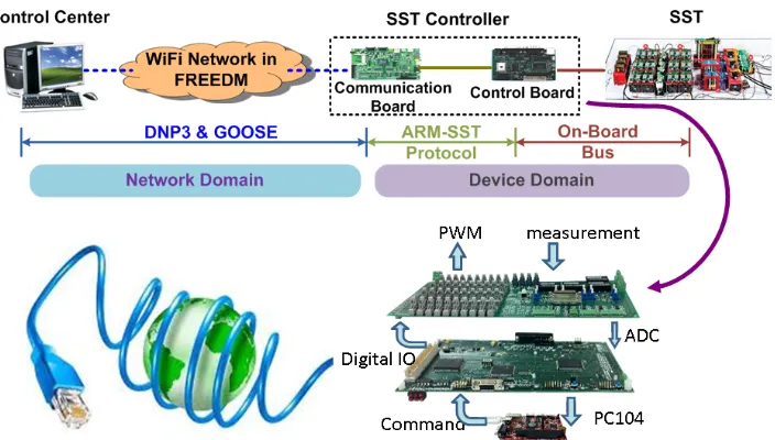
DRERs and DESDs. With the intelligent controller (Figure 1.2), each SST will have
bi-directional energy flow control capability allowing it to control active and reactive
power flow and manage to limit the fault currents on both the low voltage and high
voltage sides. Its large control bandwidth provides the plug-and-play feature for
distributed resources to rapidly identify and respond to changes in the system. With
the integrated distributed grid intelligence(DGI) hardware platform, the SST can be
monitored and controlled remotely through Ethernet.
Fig.2 SST Enabled Energy Internet
Figure 1.2: SST Enabled Energy Internet
1.2
Silicon IGBT based SST
The application of replacing 60 Hz transformer with high frequency power converters
has been discussed in many publications [38, 58, 13, 27]. There are several project
for developing the solid state transformer including UNIFLEX [8],EPRI IUT [32], GE
solid substation [20]. In 2008, FREEDM System Center has started to develop the 6.5
kV IGBT based solid state transformer (Figure 1.3). It has been rated as single phase
input voltage 7.2 kV, 60 Hz, output voltage 240/120 V, 60 Hz, 1 phase/3 wires. The
SST consists of a cascaded high voltage high frequency AC/DC rectifier that converts
60 Hz, 7.2 kV AC to three 3.8 kV DC buses, three high voltage high frequency DC-DC
converters that convert 3.8 kV to 400 V DC bus and a voltage source inverter (VSI) that
inverts 400V DC to 60 Hz, 240/120 V, 1 phase/3 wires. The switching devices in high
voltage H-bridge and low voltage H-bridges in (Figure 1.3) are 6.5 kV silicon IGBT and
600V silicon IGBT respectively. The switching frequency of the high voltage silicon
IGBT devices is 1080 Hz for the rectifier, and 3.6kHz for the DC/DC stage. The low
voltage IGBT in the VSI switches at 10.8 kHz. The silicon IGBT based SST prototype is
shown as (Figure 1.4). Due to the complexity of the topology, the control the silicon
IGBT based SST is very challenging which has been discussed in [57, 41, 56, 42, 43, 46]
Fig.1. 20kVA Solid State Transformer Topology
Figure 1.3: 6.5 kV IGBT based Solid State Transformer Topology
Fig.1. 20kVA Solid State Transformer Prototype
Figure 1.4: 6.5 kV IGBT based Solid State Transformer Prototype
1.3
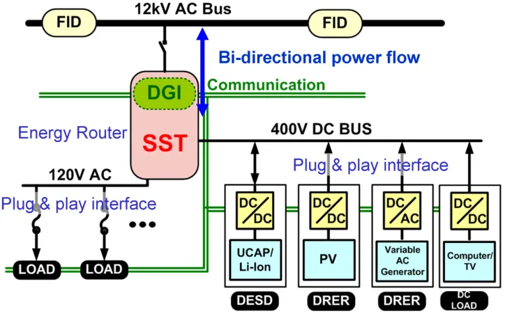
SiC Power Device based SST
With a large quantity of power devices and three cascaded stages structure for the
silicon IGBT based SST, it suffers from low efficiency and large size. With the
devel-opment of 15 kV level SiC power MOSFET, the SST topology can be simplified as in
Figure 1.5 while still provides the interface between the existing 12 kVac (7.2 kVac
L-N) istribution system and 120/240 Vac utility voltage with an extra 400 Vdc bus.
Due to SiC power MOSFET’s low loss and high switching capability, the new SST
will have reduced the size, weight and improved the efficiency. The 10A high voltage
SiC MOSFET developed by Cree Inc. has a 150um epitaxial layer which is target for
blocking 15kV. The prototype samples have been tested up to 13.5 kV, and it will be
referred to as >13 kV MOSFET in this dissertation.
+
-+
-+
-+
-L
DC/AC Inverter
Ls
Cs
Cs
Ls Dual Half Bridge
Rectifier
Figure 1.5: High Voltage SiC MOSFET based Solid State Transformer Topology
The main challenges for designing the high voltage SiC MOSFET based SST are:
(a) The power device is new and its performance has not been fully characterized.
High dv/dt generated during the switching transient may go up to 100 kV/us. For
any 10 pF parasitic coupled capacitance, 1 A current will be generated. Small coupling
capacitance will make the system packaging very difficult as well as the auxiliary
power supply design for the MOSFET gate drivers. (b) The high input voltage and
insulation voltage for the high frequency transformer will generate high electric field,
and cause partial discharge. The coupling capacitance must also be minimized because
of the high dv/dt transient of the primary terminals.
The >13 kV SiC MOSFET based SST prototype has been developed as shown in
Figure 1.6. With the limitation of the MOSFET blocking voltage, the high voltage DC
bus has been conservatively chosen as 6 kV. The new designed SST ratings are 3.6
kVac input voltage, 6kV high voltage DC bus, 400 V low voltage DC bus and 240 Vac
output with 10 kVA power rating.
xmfr
(a)
xmfr
(b)
Figure 1.6: High Voltage SiC MOSFET based Solid State Transformer Prototype Front View (a) and Back View (b)
1.4
Outline of This Dissertation
Chapter 1 introduces the solid state transformer(SST) concept and described its
function. The silicon IGBT based SST topology has been reviewed and the new
proposed SST topology based on high voltage SiC power devices is presented.
In Chapter 2, the methodology for characterizing power devices has been discussed,
followed by the characterization results of the >13 kV SiC MOSFET. It has been
identified that MOSFET’s parasitic capacitances play an important role in determining
its switching loss. A MOSFET parasitic capacitance estimation method comprising
of dynamic switching measurement and static measurement has been proposed. A
PLECS loss model has been developed and verified by the a boost converter prototype
experiment.
In Chapter 3, three different SPWM modulation methods for the full bridge rectifier
has been reviewed and the bipolar single frequency SPWM method has been identified
as the most suitable control algorithm for the >13 kV SiC MOSFET based rectifier.
With such modulation method, the generated PWM voltage frequency equals to the
switching frequency and each MOSFET equivalent switching frequency under hard
switching conditions is only 1/4 of the PWM voltage frequency. The SST rectifier
efficiency has been simulated and measured for 6 kHz and 12 kHz switching frequency
with 6 kV dc bus voltage and 3.6 kV ac voltage, which is 99.2% for 6 kHz with 8.8 kW
load and 98.5% for 12 kHz with 8.3 kW load.
In Chapter 4, The SST DC-DC stage has been designed which utilizes the dual active
half bridge (DHB) as the topology. Its zero voltage switching (ZVS) turn on range has
been analyzed and it is concluded that the dead-time and device parasitic capacitances
will reduce the ZVS range while the magnetizing current will increase the ZVS range.
For achieving ZVS operation from no load to full load, variable frequency control has
been proposed and the magnetizing inductance has been optimally designed. The
DC-DC stage efficiency has been measured as 96.9% for 10 kHz switching frequency
and 10 kW load, and the peak efficiency is 97.5% for 10 kHz switching frequency and
5 kW load.
In Chapter 5, The 1200 V 100 A SiC MOSFET module has been characterized
and compared with the same rating silicon IGBT, the PLECS loss models has been
developed for both of the devices.The inverter loss has been simulated and measured
for different switching frequency and different load.
In chapter 6, conclusions are made and future work are listed.
CHAPTER
2
Characterization of the High Voltage Power Semiconductor
Devices
2.1
Introduction
As the prerequisite for the SST circuit design, the electrical characteristics of the power
devices have to be carefully studied. These characteristics include static performance
like leakage current, forward conduction as well as dynamic performance like
switch-ing on and off. The high voltage SiC MOSFET is a new device with the state of the art
technology. It can be switched much faster than the traditional Si IGBT. There some
previous research on the 10kV SiC MOSFET [50, 51, 52, 53, 39, 40, 24, 21, 11] and 10kV
SiC JBS [15, 49]. For the >13 kV SiC MOSFET its characteristics have never been fully
studied and its application is seldom discussed. This chapter will first give a review of
power device general characterization approach, and then the performance of the >13
kV SiC MOSFET module will be studied in detail, and will be compared with the 6.5
kV Si IGBT. In the last part, a short comparison for different high voltage SiC devices
will be given.
2.2
General Approaches for Power Device
Characteriza-tion
2.2.1
Leakage Current Measurement
For power semiconductor device, static performance can be separate as DC
character-istics and AC charactercharacter-istics. DC charactercharacter-istics include blocking capability (leakage
current), output and transfer curve, on-state resistance which can all be measured by
Tektronix 370 A or 371 A curve tracer. The AC characteristic mainly means nonlinear
junction capacitances in this work which can be measured through LCR meter. Since
these characteristics are all temperature dependent, multiple measurements have to
be done under different temperature.
Since the maxim supply voltage for Tektronix 370 A curve tracer is 2 kV, the
leakage current can not be measured for voltage higher than that. Typically, the leakage
current is very small which makes it difficult to measure directly. The following circuit
(Figure 2.1) measures voltage and then calculate the current, so it can be used for
the leakage current measurement. R2 is the input impedance which is 10 MΩ for
Fluke when doing voltage measurement, R1 is used for protection once the DUT
break down, the R1 value can be hundreds of MΩwhich depends on the DUT voltage
rating. The leakage current can be calculated by (Eq. 2.1), and at the time the DUT
blocked voltage will be as in (Eq. 2.2)
Ileakage =Vmeasured/R2 (2.1)
VDUT =VDC−Ileakage·(R1+R2) (2.2)
Fig.2-1 Circuit for High Voltage Power Device Leakage Current Measurement
Figure 2.1: Circuit for High Voltage Power Device Leakage Current Measurement2.2.2
Dynamic Switching Test
The power device switching characteristics can be tested by an inductive load double
pulses tester shown as Figure 2.2[2, 9, 44], which includes a DC power supply, an
inductor, a fly wheel diode, the device under test (MOSFET for example here) and the
auxiliary circuit for providing gating signal.
CDC
L
Pulse Generator Gate Driver
VDS
Auxiliary Power
IDS VGS
D
Figure 2.2: Double Pulses Tester
Figure 2.3 displays the typical double pulse waveform, during the first gating
pulse, the MOSFET drain source current will increase linearly since the power supply
dc voltage is totally applied on the L1. By controlling the pulse width, a pre-set drain
current can be reached at the end of this pulse and the turn off transient can be
captured at this moment. Right after the first pulse, the fly wheel diode D1 will carry
all the inductor current which will keep constant if ignoring wiring resistance. The
turn on transient happens at the beginning second pulse, during which the current of
diode D1will decrease to 0 A and become reverse biased, the MOSFET carries all the
inductor current. With the variable DC voltage and first pulse width, the MOSFET
can be switched under any desired voltage and current stress.
Figure 2-3. Double Pulses Test Typical Switching Waveforms
Figure 2.3: Double Pulses Test Typical Switching Waveforms
2.3
Characterization of 6.5 kV 25 A IGBT
2.3.1
Introduction
For the given 20 kVA rating, SST requires high voltage, low current and fast switching
power devices. The commercial ABB 6.5 kV IGBT module is the best option but it has
a 200 A minimum current rating. A 6.5 kV IGBT dual module with anti-parallel diode
has been re-packaged by using ABB 6.5 kV 25 A IGBT chip and 6.5 kV 50 A diode
chip.
Figure 2.4 shows the chips layout on DCB, it contains two 25 A IGBT chips and
two 50 A diode chips. Figure 2.5 shows all module subassemblies. Figure 2.6 shows
the final prototype, for this package design, the minimum clearance distance in air is
19mm and creepage distance is 78mm which complies with IEC-60077-1 standard.
Fig.2-4 6.5kV 25A IGBT Dual Module Layout
Figure 2.4: 6.5 kV 25 A IGBT Dual Module Layout
Fig.2-5 6.5kV 25A IGBT Dual Module Subassemblies
Figure 2.5: 6.5 kV 25 A IGBT Dual Module Sub-assemblies
Fig.2-6 6.5kV 25A IGBT Dual Module Prototype
Figure 2.6: 6.5 kV 25 A IGBT Dual Module Prototype
2.3.2
Static Performance
The forward characteristics for IGBT and its parallel diode are plotted in Figure 2.7.
The leakage current for IGBT is less than 4 mA and less than 6 mA for diode.
0 5 10 15 20 25 30 35 40
0 1 2 3 4 5 6
I
F
(A
)
VF(V)
6.5kV Si IGBT and Parallel Diode I-V
6.5kV Diode 25°C 6.5kV IGBT 25°C 6.5kV Diode 125°C 6.5kV IGBT 125°C
Figure 2.7: 6.5 kV 25 A IGBT and 6.5 kV 50 A Diode I-V Curve
2.3.3
Switching Performance
The switching characteristics of this low current IGBT module have been tested with
36 mH inductive load and 100 Ω gate resistor. Figure 2.8 gives the 10 A turn on
waveform with 3.8 kV bus under 125◦C. The Turn on loss is 64.4 mJ.
Figure 2.9 shows the 5 A turn off waveform with 3 kV bus under 125◦C. The Turn
off loss is 32.7 mJ.
Fig.2-12 6.5kV 25A IGBT 3.8kV 10A Turn on
Figure 2.8: 6.5 kV 25 A IGBT 3.8 kV 10 A Turn on
Fig.2-13 6.5kV 25A IGBT 3.8kV 10A Turn off
Figure 2.9: 6.5 kV 25 A IGBT 3.8 kV 10 A Turn off
The test results under different voltage, current and temperature conditions are
plotted through Figure 2.12. Based on these test results, for 3800 V 5 A hard switching,
the total switching loss for one device under 125◦C for 1 kHz will approximately be:
Ploss = (Eon+Eo f f +Erec)×f = (46.8mJ+34.9mJ+42.3mJ)×1000=123.9(W)
(2.3)
Compromising between the system efficiency, size and thermal management
requirements, 1080 Hz has been chosen for the SST rectifier. For the DAB stage, 3 kHz
has been chosen since it is capable of ZVS under rated load.
6.5kV 25A IGBT Module Eon(mJ) vs Ice(A)
0 10 20 30 40 50 60 70 80 90 100
0 2 4 6 8 10 12 14 16
Ice(A)
Eo
n
(m
J
)
1000V 25°C 2000V 25°C 3000V 25°C 1000V 125°C 2000V 125°C 3000V 125°C
Fig.2-14 6.5kV 25A IGBT Eon(mJ) Under Different Voltages and Currents
Figure 2.10: 6.5 kV 25 A IGBTEon (mJ) under Different Voltages and Currents
6.5kV 25A IGBT Module Eoff(mJ) vs Ice(A) 0.00 10.00 20.00 30.00 40.00 50.00 60.00 70.00
0 2 4 6 8 10 12 14 16
Ice(A) Eo ff( m J ) 1000V 25°C 2000V 25°C 3000V 25°C 1000V 125°C 2000V 125°C 3000V 125°C
Fig.2-15 6.5kV 25A IGBT Eoff(mJ) Under Different Voltages and Currents
Figure 2.11: 6.5 kV 25 A IGBTEo f f(mJ) under Different Voltages and Currents
6.5kV 25A IGBT Module Erec(mJ) vs Ice(A)
0.00 10.00 20.00 30.00 40.00 50.00 60.00 70.00 80.00
0 2 4 6 8 10 12 14 16
Ice(A) Er e c (m J ) 1000V 25°C 2000V 25°C 3000V 25°C 1000V 125°C 2000V 125°C 3000V 125°C
Fig.2-16 6.5kV 25A IGBT Module Parallel Diode Erec(mJ) Under Different Voltages and Currents
Figure 2.12: 6.5 kV 25 A IGBT Module Parallel Diode Erec(mJ) under Different
Voltages and Currents
2.4
IGBT Gate Driver Design Consideration
A half bridge formed by two IGBT modules is widely used for switch characterization.
As Figure 2.13 shows, when switchS2turns on, the diodeD1will change from forward
conduction to reverse biased, and the reverse recovery current will be observed.
Fig.2-18 IGBT Switching Test Circuit Figure 2.13: IGBT Switching Test Circuit
Then turn on transient can be divided into five phases as shown in Figure 2.14:
[t0,t1]:Vge increase from 0 V to the IGBT threshold voltage; [t1,t2]: IGBT start to
conduct and the load current transferred from D1 to S2; [t2,t3]: Due to the reverse
recovery of D1, this reverse recovery current will be added to the load current and
pass through IGBT S2; [t3, t4]: Vce2 decreases near to 0 V, andVce1increases to Vbus [t4,
Eon
Vth
Vgp
Vge
Vce2
Ice2
Erec
Vka1
Ika1
Qrec
Qrec
t
0t
1t
2t
3t
4t
5Fig.2-19 IGBT Turn On Process
Figure 2.14: IGBT Turn On Process
t5]:Vge increase until the presetVge high voltage When considering the total loss of
theS1 turn on loss and D1recovery loss, it can be estimated as (Eq. 2.4):
Eon+Erec≈ Qrr·Vce+3
2
Vce·Ice2
(di/dt) +
1 2
Vce2·Ice
(dv/dt) (2.4)
According to the above equation, the loss can be reduced by increasing either
di/dt or dv/dt , which both can be achieved via reduce Rg value. However, due to
the EMI consideration, in many cases a low di/dt is preferred but high dv/dt is
acceptable. In other words, di/dt has to be reduced and dv/dt can be increased for
the loss minimization purpose. A circuit has been proposed as in Figure 2.13, An
extra inductor has been put in series with the IGBT emitter, when there is a positive
di/dt the inductor induced voltage will pull out current from the IGBT gate which
will reduceVge, consequently decrease di/dt.
Vge
Ice
Vce
-V
LeFig.2-20 IGBT Turn On (Rg=100ohm, Le=100nH, ZD1 disconnected, di/dt=180A/us, Eon=40.6mJ)
Figure 2.15: IGBT Turn On (Rg=100 ohm,Le=100 nH, without Zener)
Figure 2.15 gives the turn on waveform when disconnect the ZD1, theLe voltage is
proportional to the Ice slope.
Vge
Ice
Vce
-VLe
Fig.2-21 IGBT Turn On (Rg=100ohm, Le=100nH, di/dt=52.6A/us, Eon=49.5mJ)
Figure 2.16: IGBT Turn On (Rg=100 ohm, Le=100 nH, with Zener)
Figure 2.16 gives the turn on waveform when connect the ZD1, thedi/dt has been
reduced from 180 A/us to 52.6 A/us compared with Figure 2.15.
Figure 2.17 gives the turn on waveform when change Rg from 100Ωto 10Ω, the
di/dt is about the same as Figure 2.16, but dv/dt has increased about two times, and
the loss decreased to 37.1 mJ from 49.5 mJ.
Based on above analysis, IGBT turn on transient speed is dependent on the gating
voltage and current, for the IGBT turn off transient speed, it is determined by the
IGBT itself. The turn off transient can be divided as voltage increase phase and current
falling phase, there time periods are given by equation Eq. 2.5 and Eq. 2.6
Vge
Ice
Vce
-VLe
Fig.2-22 IGBT Turn On (Rg=10ohm, Le=100nH, di/dt=56.6A/us, Eon=37.1mJ)
Figure 2.17: IGBT Turn On (Rg=10 ohm,Le=100 nH, with Zener)
tV,OFF = εs
·pW NB+·VCS
WN·(ND +pSC)·JC,ON (2.5)
τI,OFF =τP0,NB·ln(10) = 2.3τP0,NB (2.6)
The test waveforms in Figure 2.18 and Figure 2.19 prove the Rg has little impact
on the IGBT turn off speed.
In conclusion, the 6.5 kV silicon IGBT turn on loss can be reduced by proper
design of the gate driver while the turn off loss is determined by the IGBT internal
parameters.
Vge
Ice
Vce
Fig.2-23 IGBT Turn Off (Rg=10ohm, dv/dt=3.18kV/us, Eon=24.5mJ)
Figure 2.18: IGBT Turn Off (Rg=10 ohm,dv/dt=3.18 kV/us, Eon=24.5 mJ)
Vge
Ice
Vce
Fig.2-24 IGBT Turn Off (Rg=220ohm, dv/dt=3.23kV/us, Eon=22.6mJ)
Figure 2.19: IGBT Turn Off (Rg=220 ohm,dv/dt=3.23 kV/us, Eon=22.6 mJ)
2.5
Characterization and Modeling of 13 kV 10 A SiC
MOSFET
2.5.1
Introduction
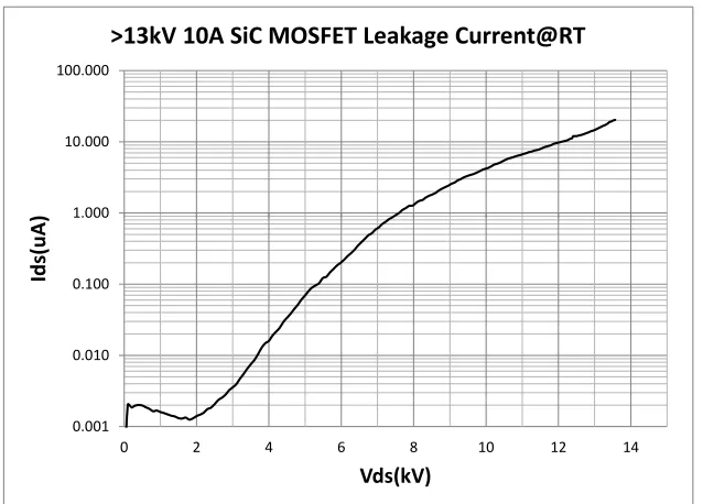
The >13 kV SiC MOSFET and JBS developed by Cree Inc. has a 150um n-type SiC
epilayer as the drift layer to support the high voltage as shown in Figure 2.20. The
designed voltage blocking capability is higher than 15 kV, but the blocking voltage
has only been tested up to 13.5 kV with 20 uA leakage current (Figure 2.22) for the
safety concern. The MOSFET has a die size of 8.1mm×8.1mm, and the JBS has a die
size of 8.1mm×10.0mm.
Gate
Drain
Source
N- drift region
N+ Substrate
N+
P-Base
R
CHR
DR
CHR
J150um epi-layer
Figure 2.20: Simplified >13 kV SiC MOSFET Cross Section
One MOSFET chip and one JBS chip has been packaged together as a module.
Because of the poor performance of the MOSFET body diode, a silicon diode has been
put in series with the MOSFET in order to block the conduction of the SiC MOSFET
body diode. Fig shows the schematic and package layout. The final module has a size
of 80mm×43mm×15.8mm.
Fig.2-25 15kV SiC 10A Mosfet Module Schematic and Prototype
(a)
Fig.2-25 15kV SiC 10A Mosfet Module Schematic and Prototype
(b)
Figure 2.21: >13 kV SiC 10 A MOSFET Module Schematic and Prototype
2.5.2
Static Characteristics
The blocking characteristics of the >13 kV MOSFET as in Figure 2.22, measured at
room temperature with 0 V gate bias, shows that the leakage current is only 20 uA at
13.5 kV blocking voltage.
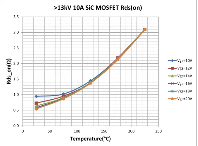
The typical on-state characteristics of the >13 kV SiC MOSFET measured for
different temperatures and different gate voltages is shown in Figure 2.23. With 20 V
0.001 0.010 0.100 1.000 10.000 100.000
0 2 4 6 8 10 12 14
Ids(uA)
Vds(kV)
>13kV 10A SiC MOSFET Leakage Current@RT
Figure 2.22: >13 kV SiC 10 A MOSFET Module Leakage Current
gate bias, the Rds(on) is 0.55 Ω at 25◦C and 1.7Ωat 125◦C . It is can be found that
forward on resistance is highly dependent on the gate bias for low temperature and
almost keeps constant for high temperature with different gate bias.
The MOSFET on-resistance mainly contains three parts: channel resistance (Rch),
JFET region resistance (RJFET), and drift region resistance (Rd). The channel resistance
is determined by the gate bias and has a negative temperature coefficient (PTC), the
JFET and drift region resistances will not be affected by the gate bias and both have
a negative temperature coefficient (NTC). Unlike the 1200 V SiC MOSFET, >13 kV
MOSFET has a very thick drift layer, the drift region resistance dominant within the
total loss. Especially for the higher temperature, the channel resistance will reduce
and the JFET and drift region resistance will increase, the channel resistance variance
caused by gate bias will make little impact on the total on-resistance. For the power
circuit applications, the MOSFET junction temperature normally around 125◦C during
operation, the conduction loss will not be reduced by having a higher gate driver
voltage for the >13 kV SiC MOSFET. However, for the 1200 V MOSFET, it is suggested
to apply 20 V gate bias for minimizing conduction loss.
0.0 0.5 1.0 1.5 2.0 2.5 3.0 3.5
0 50 100 150 200 250
Rds
_on(
Ω
)
Temperature(°C)
>13kV 10A SiC MOSFET Rds(on)
Vgs=10V Vgs=12V Vgs=14V Vgs=16V Vgs=18V Vgs=20V
Figure 2.23: >13 kV SiC 10 A MOSFET V-I Curves
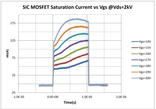
On the other hand, the gate bias voltage will determine the MOSFET saturation
current, the higher gate bias voltage will have high saturation current as shown in
Figure 2.24. The MOSFET short circuit capability is typically thermally limited, and
the energy dissipated in the MOSFET is [26]:
Esc =
Z t1+tsc
t1
Vsc·Isc·dt (2.7)
The MOSFET short circuit voltage usually will be the DC bus voltage. With same
short circuit energy limit, the short circuit time can be longer if the short circuit current
-25 25 75 125 175
-1.0E-05 0.0E+00 1.0E-05 2.0E-05
Id
s(A)
Time(s)
SiC MOSFET Saturation Current vs Vgs @Vds=2kV
Vgs=14V Vgs=15V Vgs=16V Vgs=17V Vgs=18V Vgs=19V Vgs=20V
Figure 2.24: SiC MOSFET Saturation Current vs Gate Voltage
is lower. From protection point of view, a lower gate voltage bias will give a longer
short circuit protection time and ease the protection circuit design.
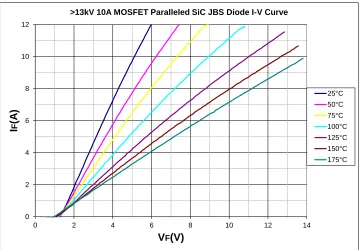
The typical forward characteristics of the paralleled >13kV SiC JBS diode measured
for different temperatures is shown in Figure 2.25, the device forward voltage at the
rated current of 10 A is 5.2 V under 25◦C and 11 V under 125◦C. The I-V curve can
be simply described as the Eq. 2.8 for 25◦C and Eq. 2.9 for 125◦C
VF =0.43×IF +0.95 (2.8)
VF =1.025×IF+0.75 (2.9)
0 2 4 6 8 10 12
0 2 4 6 8 10 12 14
I
F
(A
)
VF(V)
>13kV 10A MOSFET Paralleled SiC JBS Diode I-V Curve
25°C 50°C 75°C 100°C 125°C 150°C 175°C
Figure 2.25: >13 kV SiC 10 A JBS Diode I-V Curves for Different Temperature
2.5.3
Switching Transient and Loss analysis
For the low voltage silicon MOSFET, its switching process under clamped inductive
load has been analyzed in many publications [37, 54], since the energy stored by the
low voltage MOSFET junction capacitor is negligible, and the current used to charge
or discharge the output capacitor is small enough compared with the load current,
so the MOSFET channel current can be consider approximately equal to its drain
current when analyzing the switching transient. The MOSFET switching transient
can be separated into four different phases for both turn on and turn off as shown in
Figure 2.26
The four phases for turn on are: Phase I [t0, t1]: At t0, the gate driver starts to
charge the Cgs andCgd, the MOSFET will not turn on until t1 when theVgs reaches
the threshold voltage Vth. Phase II [t1, t2]: Att1, the MOSFET starts to turn on, drain
Eon Vth Vgp Vgs Vds Ids Igs Io
QGS QGD QG
t0 t1 t2 t3
t t4 QG(sw) (a) Vth Vgp Vgs Vds Igs Io QGS QGD QG
t5 t6 t7 t8 t9 t
Eoff
Ids
QG(sw)
(b)
Figure 2.26: Si MOSFET Turn on and Turn off
current increases; the load current transfers from the free-wheel diode to the MOSFET,
this process will finish at t2when all load current has been transferred. During this
stage: Ids =gm(Vgs−Vth)
Phase III [t2,t3]: Att2, the MOSFET drain current has reached the inductive load
current, Vds starts to decrease, the gate source voltage shows the miller plateau which
isVgs =Ids/gm+Vth, and the gate current determines thedv/dtslope of the Vds , this
phase will be ended at t3 when Vds reached 0V Phase IV [t3,t4]: At t3, the MOSFET
has been fully turned on, with continuously increasing theVds , the channel resistance
can be further reduced, and finally Vgs will be equal to the gate driver high output
voltage. The total turn on loss will be:
Eon = 1
2·Vin·Iin·(t2_1+t3_2) ≈ 1
2 ·Vin·Iin·
QSW
IG(L−H)
(2.10)
The four phases for turn off are identical as the turn on, the turn off loss can be
calculated as:
Eo f f = 1
2 ·Vin·Iin·(t7_6+t8_7)≈ 1
2·Vin·Iin·
QSW
IG(H−L)
(2.11)
The total switching loss:
Esw = Eo f f +Eo f f ≈ 1
2·Vin·Iin·(
QSW
IG(L−H)
+ QSW
IG(H−L)
) (2.12)
However, for the high voltage low current SiC MOSFET, the parasitic capacitors
store a significant amount of energy, and the required current used to charge or
discharge the output capacitance is comparable to the drain current, the previous
analysis method will become invalid for estimation switching loss. The MOSFET
parasitic capacitances can be represented by three equivalent capacitors Cgs, Cgd ,Cds
and
Ciss =Cgs+Cgd (2.13)
Crss=Cgd (2.14)
Coss =Cds+Cgd (2.15)
For the high voltage SiC power devices, Coss will contribute a large portion of the
switching loss because a large amount of energy has been stored byCoss.
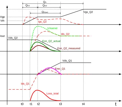
The turn on process shown in Figure 2.27 is similar as the previous case which
ignores junction capacitances, the only difference is in phase III,
Eon_Q2_measured
Vth Vgp
Vgs_Q2
Vds_Q2
Ids_Q2 Igs_Q2
Ids_Q1
Vds_Q1
Erec_Q1
Loss_total
Iout
QGS QGD
QG
Ichannel
Eon_Q2_actual
t0 t1 t2 t3 t4
t
QG(sw)
Figure 2.27: MOSFET Turn on Process
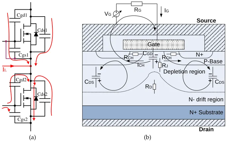
During Phase III,Vds drops from Vin to 0 V, which meansCgd2, CCds2is charging,
However theCgd2 and CCds2 discharging current will be inside the MOSFET as shown
in Figure 2.28 and cannot be measured through the drain or source terminal. This part
of capacitive energy loss will not be counted in the measured turn on loss.
IL
Cds1 Cgd1
Cgs1
Cds2 Cgd2
Cgs2
(a)
Gate
Drain Source
N- drift region
N+ Substrate N+
P-Base RCH
RD
RG
VG IG
ICH
Depletion region RCH
CDS CDS
CGD
RJ
(b)
Figure 2.28: MOSFET Internal Parasitic Capacitance Discharging During Turn on
When considering a half bridge configuration of the SiC MOSFET module, the top
module output capacitor
Coss1 =Cds1+Cgd1 (2.16)
the bottom module output capacitor
Coss2 =Cds2+Cgd2 (2.17)
Coss1=Coss2 (2.18)
Let us first consider the output capacitor related losses, it is well known that
the energy stored in a linear capacitor is Ecap(V) = 12C·V2 and charge Q = C∗V,
for an RC circuit as in Figure 2.29(a), the energy dissipated on the resistor equals
to the energy stored in the capacitor during the charging. But the MOSFET output
capacitance is nonlinear and has strong bias voltage dependency. If considering the
nonlinear case as shown in Figure 2.29(b),
C(V) = √1
V (2.19)
Capacitor stored charge,
Q(V) =
Z V
0 C(v)dv =
Z V
0 1 √
vdv=2
√
V (2.20)
Capacitor stored energy:
Ecap(V) = Z V
0 V(Q)dq =V·Q(V)−
Z V
0 Q(v)dv
=V·(2√V)−(4
3V 3/
2) = 2
3V 3/
2 = 2
3[C(V)]
−3
(2.21)
Total energy supplied by the source:
Es(V) =V·Q(V) (2.22)
The energy dissipated by R will be:
ER(V) = Es(V)−Ecap(V) = V·Q(V)−2
3V 3/
2 = 4
3V 3/
2 = 4
3[C(V)]
−3
(2.23)
It can found from the above equations that the energy dissipated on the resistor is
two times of the energy stored in the capacitor during the charging process.
Vs
C R S
Vs
R S
C R S
Is
(a) (b) (c)
Figure 2.29: RC Charging Circuit
If using a current source to charge a capacitor (Figure 2.29(c)), then
V = I
C ·t (2.24)
Ecap(V) =V·Q(V) = (I
C ·t)·(I·t) =
1
C ·(I·t)
2 = 1
2 ·C·V
2 (2.25)
ER(V) = I2·R·t (2.26)
According to the above analysis, when a capacitor is charged by a voltage source,
the energy loss will be independent of the charging current, and the amount of the
loss will beV·Q(V)−E(V), but if the capacitor is charged by a current source, the
energy loss will be determined by the charging current and the series resistance.
So the above turn on loss can be separated into three parts:1) switching loss
without considering Coss which is V·Q(V)−E(V), 2) the stored energy Eoss2 by
Coss2 3) the extra current for charging Coss1 caused loss which can be calculated as
Qoss1·Vin−Eoss1
Since Eoss1 =Eoss2, The total turn on loss will be:
Eon = 1
2 ·Vin·Iin·
QSW
IG(L−H)
+Qoss·Vin (2.27)
While the measured turn on loss will only be:
Eon(measured) = 1
2 ·Vin·Iin·
QSW
IG(L−H)
+Qoss·Vin−Eoss (2.28)
From the above equation, we can find the turn on loss is highly independent on
the gate driver current, smaller gate resistor will have larger drive current and higher
miller plateau as shown in Figure 2.30 which gives the Vgs waveforms for a gate
resistor of 10Ω, 22Ω, 56Ωso as the turn on speed shown in Figure 2.31
The measure turn on loss for 6 kV Vds are plotted in Figure 2.32 which shows the
turn on loss dependency on the gate resistor. It can also be found the minimum turn
on loss during 0 A current turn on is constant for different gate resistors, this loss is
the energy caused by the MOSFET module output capacitors, the amount is about 6
mJ and can be calculated as Qoss·Vin−Eoss without including the MOSFET internal
energy loss.
-10 -5 0 5 10 15 20
0 0.2 0.4 0.6 0.8 1 1.2 1.4 1.6 1.8 2
V
gs(V
)
Time(us)
>13kV SiC MOSFET Turn On for Different Rg
Vgs-Rg=10Ω Vgs-Rg=22Ω Vgs-Rg=56Ω
Figure 2.30: SiC MOSFET Turn on for Different Rg
-5 0 5 10 15 20 25 30 35 -1 0 1 2 3 4 5 6 7
0 0.2 0.4 0.6 0.8 1 1.2 1.4 1.6 1.8 2
Ids( A) V ds(kV ) Time(us)
>13kV SiC MOSFET Turn On for Different Rg
Vds-Rg=10Ω Vds-Rg=22Ω Vds-Rg=56Ω Ids-Rg=10Ω Ids-Rg=22Ω Ids-Rg=56Ω
Figure 2.31: SiC MOSFET Turn on for Different Rg
0 5 10 15 20 25 30 35 40
0 2 4 6 8 10 12
Eon
(mJ
)
Ids(A)
>13kV SiC MOSFET Eon@6kV, 25°C
Rg=10Ω
Rg=22Ω
Rg=56Ω
Figure 2.32: SiC MOSFETEon
The turn off transient can also be divided into four phases as shows in Figure 2.33
which is different from the low voltage silicon MOSFET turn off transient. Phase I [t5,
t6]: Vgs starts to decrease att5, the MOSFET drain current will keep unchanged until
t6 whereVgs reachVgp, hereVgp is the minimum gate voltage to maintain the drain
current.
Phase II [t6,t7]: For low voltage MOSFET, the Vds will increase while the Ids will
keep constant during this phase, while for the >13 kV SiC MOSFET, the load current
will also be used for charging the output capacitance. If assuming output capacitance
is constant:
IL = Ichannel+Coss2· dVds2
dt +Coss1·
dVds1
dt = Ichannel+2·Coss2· dVds2
dt (2.29)
Ichannel Vth
Vgp
Vgs_Q2
Vds_Q2
Ids_Q2 Igs_Q2
Ids_Q1
Vds_Q1
Iout
QGS
QGD
QG
t5 t6 t7 t8 t9
t
Eoff_Q2_actual
Eoff_Q2_measured
Energy recovered
Loss_total
Figure 2.33: MOSFET Turn off Process
−Igd2=Cgd2
dVds2
dt =
Cgd2 2·Coss2
·(IL−Ichannel) (2.30)
Since Coss2 is typical about 10 times of Cgd2 for the SiC MOSFET, For 10A load
current,
−Igd2 =
Cgd2 2·Coss2
·(IL−Ichannel) <
1
2·10 ·(10−0) = 0.5A (2.31)
The above equation indicates with no channel current and all load current is used for
chargingCoss2 and discharging Coss1, the maximum drain gate current is 0.5 A, if the
gate driver sink current is higher than 0.5 A, the Vgs will be discharged to a value less
the threshold voltage, when the channel current becomes 0 A. This transient is very
fast with properly chosen Rg(o f f) and during this time theVds is still almost zero, so
Eo f f(t7_6)≈0
Phase III [t7,t8]: Att7, the MOSFET channel has been reached 0, for phase 3, the
load current will be divided by the parasitic capacitors as shown in Figure 2.33 and
Figure 2.34
Igd2 =
Cgd2
Coss1+Coss2
·IL (2.32)
Ids2 =
Cds2
Coss1+Coss2
·IL (2.33)
Ioss1= Coss1
Coss1+Coss2
·IL (2.34)
Eo f f_measured(t8_7) =
Z t8
t7 Vds
·Id·dt =Eoss2 (2.35)
IL Cds1 Cgd1 Cgs1 Cds2 Cgd2 Cgs2 IL Cds1 Cgd1 Cgs1 Cds2 Cgd2 Cgs2 (a) Gate Drain Source
N- drift region
N+ Substrate N+ P-Base RCH RD RG VG IG ICH Depletion region RCH CDS CDS CGD RJ (b)
Figure 2.34: MOSFET Internal Parasitic Capacitance Discharging During Turn off
Phase IV [t8, t9]:
At t8, Vds reachVin, the fly-wheel diode starts to conduct, andVgs drops to the gate
driver turn off voltage. The total measured turn off loss is Eoss2 while the actual loss
which converted to heat is negligible.
Esw(measured) =Eon(measured)+Eo f f(measured) = 1
2 ·Vin·Iin·
QSW
IG(L−H)
+Qoss·Vin =Eon
(2.36)
Though the total measured loss equals the total actual loss, the loss energy has
only been converted to the heat during the turn on. So for the zero voltage turn on
application, the switching loss will virtually be zero.
The SiC MOSFET module turn off has been tested with a turn off gate resistance
of 1Ω, 10Ω, 22Ω, 56Ω separately, the switching waveforms have been plotted in
Figure 2.35 and Figure 2.36, the measured turn off loss has been plotted in Figure 2.37.
-10.0 -5.0 0.0 5.0 10.0 15.0 20.0
0.0 0.2 0.4 0.6 0.8 1.0 1.2 1.4 1.6 1.8 2.0
V
gs(V
)
Time(us)
>13kV SiC MOSFET Turn Off for Different Rg
Vgs-Rg=10Ω Vgs-Rg=22Ω Vgs-Rg=56Ω Vgs-Rg=1Ω
Figure 2.35: SiC MOSFET Turn off for Different Rg
-2 0 2 4 6 8 10 12 14 -1.0 0.0 1.0 2.0 3.0 4.0 5.0 6.0 7.0
0.0 0.2 0.4 0.6 0.8 1.0 1.2 1.4 1.6 1.8 2.0
Ids(A) V ds (kV ) Time(us)
>13kV SiC MOSFET Turn Off for Different Rg
Vds-Rg=1Ω Vds-Rg=10Ω Vds-Rg=22Ω Vds-Rg=56Ω Ids-Rg=1Ω Ids-Rg=10Ω Ids-Rg=22Ω Ids-Rg=56Ω
Figure 2.36: SiC MOSFET Turn off for Different Rg
0 1 2 3 4 5 6 7 8 9 10
0 2 4 6 8 10 12
Eoff
(mJ)
Ids(A)
>13kV SiC MOSFET Eoff@6kV, 25°C
Rg=1Ω
Rg=10Ω
Rg=22Ω
Rg=56Ω
Figure 2.37: SiC MOSFET Turn off Energy for Different Rg
2.5.4
MOSFET Parasitic Capacitances Measurement
As per the analysis in the previous sections, the high voltage MOSFET output
capac-itance stores a significant amount of energy. Hence it is critical to have an accurate
estimation of its value. Due to the nonlinear characteristic, the capacitance will be
different for different voltage bias. The LCR meter or impedance analyzer usually
can only generated 40 V bias which is much below the device rated voltage. For the
higher voltage measurement, some methods have been proposed in [3, 36, 18], all of
these solutions are based on the static measurement through impedance analysis and
requires some external circuits including high voltage bias. These circuits are complex
and have poor capacitance measurement accuracy.
The output and reverse transfer capacitance can also be estimated through the
dynamic switching test. As shown in Figure 2.39 The top MOSFET gate source is
shorted, when the bottom MOSFET switches from off to on status, the top MOSFET
Cgd1 and Cds1 will be charged, the waveforms of Vds1, Id1 and Igd1 can be captured
through the oscilloscope, and then the capacitance can be calculated as:
Coss = Id1/( dVds1
dt ) (2.37)
Coss = Id1/(
dVds1
dt ) (2.38)
Due to the probe’s measurement resolution, the calculated capacitance will include
large error when the measured drain source voltage is low. A combination method
should be used which includes both the static measurement for low voltage bias and
the dynamic switching test for high voltage bias. First of all, the MOSFET capacitance
can be predicted by Eq. 2.39,
C(V) = √ k
V+Vbi
(2.39)
Considering some packaging related capacitance , the equation becomes:
C(V) = √ k
V+Vbi
+Co (2.40)
So,
Coss(V1)−Co Coss(V2)−Co
=
√
V2+Vbi
√
V1+Vbi
(2.41)
Coss(V1) = √
V2+Vbi
√
V1+Vbi
·(Coss(V2)−Co) +Co (2.42)
With all capacitances which has measured up to 40V bias, the Vbi, Co in the above
equation can be solved. However, Co is much smaller than the output capacitance
with less than 40V voltage bias, its value should be calibrated by the high voltage
dy-namic switching test results. The finale estimations areCoss(37.3) = 859pF, Vbi =2.3,
Co =30pFand the output capacitance has been plotted in Figure 2.38 and accordingly
the output capacitor stored charge and energy can be calculated.
10 100 1000 10000
0 20 40 60 80 100
Capa cit anc e( pF ) Vds(V)
>13kV SiC MOSFET Module Output Capacitance
Coss-measured Coss-estimated (a) 10 100 1000 10000
0 2000 4000 6000 8000 10000 12000
Capa cit anc e( pF ) Vds(V)
>13kV SiC MOSFET Module Output Capacitance
Coss-measured Coss-estimated
(b)
Figure 2.38: SiC MOSFET Output Capacitance (Coss)
The above estimation needs to be verified by the dynamic measurement with the
pulse test circuit shown in Figure 2.39. and one single gating pulse has been applied
Figure 2.40. During the turn on,
Z
Ids2·dt =Qoss1(Vin) +Cp·Vin (2.43)
Z
Vds2·Ids2·dt =Qoss1·Vin−Eoss1(Vin) +1
2·Cp·V 2
in (2.44)
During the turn off, if the turn off gate resistance small enough,
Z
Ids2·dt =Qoss2(Vin) (2.45)
Z
Vds2·Ids2·dt= Eoss2(Vin) (2.46)
CDC
Lp
Rdischarge
Cp
Cds2 Cgd2
Cgs2
Cds1 Cgd1
Cgs1
Input DC Voltage
Q2
Pulse Generator Gate Driver
VDS
Auxiliary Power
IDS VGS
Q1
Figure 2.39: SiC MOSFET Double Pulse Test Circuit
The output capacitor energy and charge can also be calculated by its capacitance:
Qoss(Vin) = Z Vin
0 Coss(V)·dv (2.47)
>13kV SiC MOSFET Characteristics: Coss Estimation
Ids
Vds
Vgs
Energy
Figure 2.40: SiC MOSFET 0A Turn on and off Waveforms
Eoss(Vin) = Z Vin
0 V(Q)dq=Vin·Qoss(Vin)−
Z Vin
0 Qoss(v)dv (2.48)
In Figure 2.41 the output capacitor charge has been estimated based on the output
capacitance model for 1 kV to 12 kV drain voltage bias, the dynamic measurement
data has been taken for the drain voltage 3 kV to 6 kV, it shows a good match.
In Figure 2.42 the output capacitor stored energy (Eo f f in the figure) and the
dissi-pated energy for charging the output capacitor(Eon in the figure) has been estimated
based on the output capacitance model for 1 kV to 12 kV drain voltage, the dynamic
measurement data has been taken for the drain voltage 3 kV to 6 kV, which matches
with the estimated loss perfectly.
0 200 400 600 800 1,000 1,200 1,400 1,600
0 2 4 6 8 10 12 14
Qoss(nC)
Vds(kV)
>13kV SiC MOSFET Module Output Capacitance Charge
Qoss-estimated Qoss-measured
Figure 2.41: SiC MOSFET 0 A Turn on and off Waveforms
0 2 4 6 8 10 12 14 16 18 20
0 2 4 6 8 10 12 14
En
ergy
(mJ)
Vds(kV)
>13kV SiC MOSFET Module Capacitive Switching Loss
Eoff-estimated Eoff-measured Eon-estimated Eon-measured
Figure 2.42: SiC MOSFET Capacitive Switching Loss
2.5.5
MOSFET Loss Model
The switching loss for the high voltage SiC MOSFET only contains turn on loss which
can be calculated by the following equation
Eon = 1
2 ·Vin·Iin·
QSW
IG(L−H)
+Qoss·Vin =
1
2 ·Vin·Iin·ton+Qoss·Vin (2.49)
The output capacitor Qoss has been estimated based on the output capacitance.
The turn on time ton has been measured for the drain voltage up to 6 kV with a gate
resistance of 10Ωas shown in Figure 2.43, the linear turn on time increase from 3 kV
to 6 kV drain voltage has been observed for different drain current, and for the higher
drain voltage, theCgd decrease very slightly, it is fair to estimate that the turn on time
will increase linearly for voltage high than 6 kV and up to 12 kV.
0 100 200 300 400 500 600 700 800 900
0 2 4 6 8 10 12 14
Tur
n
on Time(ns)
Vds(kV)
>13kV MOSFET Module Turn on Time
10A-measured 10A-estimated 8A-measured 8A-estimated 6A-measured 6A-estimated 4A-measured 4A-estimated 2A-measured 2A-estimated
Figure 2.43: SiC MOSFET Turn on Time