A Reconfigurable Cache for Efficient Use of Tag RAM as
Scratch-Pad Memory
Kamarthi Prakash Kumar1, S.Ashok Reddy2, S.Mahaboob Basha3 1
P.G. Scholar, 2Assistant Professor, 3Head of the Department
1,2,3
Branch:ECE ( VLSI )
GEETHANJALI COLLEGE OF ENGG. & TECH.
Email id:[email protected],[email protected]
Abstract
The cache memory has been a predominant component in modern chips, easily taking up more than 50% of the silicon area. It is then desirable to make the cache memory flexible for different needs. Therefore, many modern processor chips allow users to configure a part of the cache memory as the scratch-pad memory (SPM), a high-speed internal memory for rapid data access. However, such approach uses only the data RAM of the cache memory while leaving the tag RAM unused and thus wasting its capacity. This paper presents a cache organization, called Tag-SPM architecture, which allows the tag RAM to be used as the SPM and thus increases its capacity. It is accomplished with small Tag/Data-SPM controllers and four additional multiplexers in the cache organization. The proposed Tag-SPM architecture has been implemented with an academic ARM-based microprocessor with 4-/4-kB four-way set associative instruction/data caches at the register transfer level. Experiments show that the proposed architecture boosts the SPM capacity by 12.5% and requires only 0.08% area (434 gates) overhead without impairing the cache’s circuit speed in TSMC’s 90-nm standard cell implementation. Furthermore, the power overhead is negligible. When the Tag-SPM architecture is applied to typical cache systems, such as in ARM’s Cortex-A5 and Cortex-A53 processors, additional 12.5% SPM space per way can also be gained in both cases. The analyses show that our
Tag-SPM architecture is a highly cost-effective way to boost the SPM space.
Keywords-Cache memory, microprocessor, reconfigurable, architecture, system-on-chip.
INTRODUCTION
manipulated well, its performance could be better than the cache.
Since the cache and the SPM have their own advantages and usage scenarios, many microprocessor/DSP/GPU cores, such as Intel’s XScale, Texas Instruments’ TMS320C62, and NVidia’s Fermi , have configurable caches, which allow the programmer to configure a part of the cache to operate as an SPM (or called tightly coupled memory). Under such SPM mode, only the data RAM of the cache memory is utilized; the tag RAM of such cache is not used and thus wasted.
In this project, we propose a cache organization, called Tag-SPM architecture, which allows its tag RAM to be used as the SPM as well and thus increases the SPM capacity in a highly cost-effective way. To the best of our knowledge, this is the first work to address such issue.
On chip caches using static RAM consume power in the range of 25% to, 45% of the total chip power. Recently, interest has been focused on having on chip scratch pad memory to reduce the power and improve performance. On the other hand, they can replace caches only if they are supported by an effective compiler. Current embedded processors particularly in the area of multimedia applications and graphic controllers have on-chip scratch pad memories. In cache memory systems, the mapping of program elements is done during runtime, whereas in scratch pad memory systems this is done either by the user or automatically by the compiler using suitable algorithm.
LITERATURE SURVEY
Ing-Jer Huang received the B.S. degree in electrical Engineering from National Taiwan University, Taipei, Taiwan, in 1986, and the M.S. and Ph.D. Degrees in computer engineering from the University of Southern California, Los Angeles, CA, USA, in 1989 and 1994, respectively. He is currently a Professor with the Department
of Computer Science and Engineering, National Sun Yat-sen University, Kaohsiung, Taiwan. His current research interests include microprocessors, systemon-chip design, design automation, system software, embedded systems, hardware/software code sign, academic and industrial activities, and extensive collaboration with several IC-related industries. Dr. Huang is a member of the ACM.
Chun-Hung Lai received the B.S.
degree Information Engineering and Computer Science, Feng-Chia University, Taichung, Taiwan, and the M.S. and Ph.D. degrees from National Sun Yat-sen University, Kaohsiung, Taiwan, in 2007 and 2014, respectively. He is currently an Engineer with the Industrial Technology Research Institute, Hsinchu, Taiwan. His current research interests include systemon-chip debugging methodology, microprocessor design or verification, and multipurpose cache architecture.
Yun-Chung Yang received the B.S. and M.S.degrees from the Department of Computer Science and Engineering, National Sun Yat-sen University, Kaohsiung, Taiwan, in 2011 and 2015, respectively. He is currently an Engineer with the Design Validation Department, Elite Semiconductor Memory Technology Inc., Hsinchu, Taiwan. His current research interests include memory issues in embedded system design, embedded microprocessors, and hardware/software codesign.
MEMORY RAM
consecutively, because of mechanical design limitations. Therefore the time to access a given data location varies significantly depending on its physical location.
Today, random-access memory takes the form of integrated circuits. Strictly speaking, modern types of DRAM are not random access, as data is read in bursts, although the name DRAM / RAM has stuck. However, many types of SRAM, ROM, OTP, and NOR flash are still random access even in a strict sense. RAM is normally associated with volatile types of memory (such as DRAM memory modules), where its stored information is lost if the power is removed. Many other types of non-volatile memory are RAM as well, including most types of ROM and a type of flash memory called NOR-Flash. The first RAM modules to come into the market were created in 1951 and were sold until the late 1960s and early 1970s.
RAM is small, both in terms of its physical size and in the amount of data.
RAM is of two types 1. Static RAM (SRAM) 2. Dynamic RAM (DRAM)
3.1.1 Static RAM (SRAM)
The word static indicates that the memory retains its contents as long as power remains applied. However, data is lost when the power gets down due to volatile nature.
It has long data lifetime
There is no need to refresh
Faster
Used as cache memory
Large size
Expensive
High power consumption
Dynamic RAM (DRAM) DRAM
Unlike SRAM, must be continually refreshed in order for it to maintain the data. This is done by placing the memory on a refresh circuit that rewrites the data several
hundred times per second. DRAM is used for most system memory because it is cheap and small. All DRAMs are made up of memory cells. These cells are composed of one capacitor and one transistor.
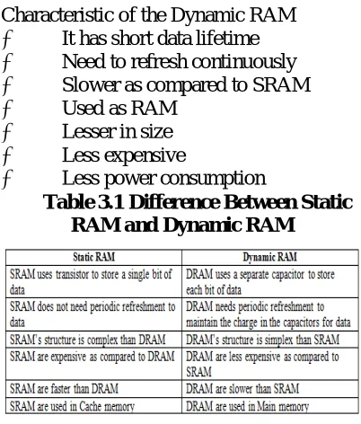
Characteristic of the Dynamic RAM
It has short data lifetime
Need to refresh continuously
Slower as compared to SRAM
Used as RAM
Lesser in size
Less expensive
Less power consumption
Table 3.1 Difference Between Static RAM and Dynamic RAM
3.2 Read-only memory (ROM) is a class of storage medium used in computers and other electronic devices. Data stored in ROM cannot be modified, or can be modified only slowly or with difficulty, so it
is mainly used to
distribute firmware (software that is very closely tied to specific hardware, and unlikely to need frequent updates).
In its strictest sense, ROM refers only to mask ROM (the oldest type of solid state ROM), which is fabricated with the desired data permanently stored in it, and thus can never be modified. Despite the simplicity, speed and economies of scale of mask ROM, field-programmability often make reprogrammable memories more flexible and inexpensive. As of 2007, actual ROM circuitry is therefore mainly used for applications such as microcode, and similar structures, on various kinds of processors.
and electrically erasable programmable read-only memory (EEPROM or Flash ROM) are sometimes referred to, in an abbreviated way, as "read-only memory" (ROM); although these types of memory can be erased and re-programmed multiple times, writing to this memory takes longer and may require different procedures than reading the memory.[1] When used in this less precise way, "ROM" indicates a non-volatile memory which serves functions typically provided by mask ROM, such as storage of program code and nonvolatile data.
Use for Storing Program
Every stored-program computer needs some form of non-volatile storage (that is, storage that retains its data when power is removed) to store the initial program that runs when the computer is powered on or otherwise begins execution (a process known as bootstrapping, often abbreviated to "booting" or "booting up"). Likewise, every non-trivial computer needs some form of mutable memory to record changes in its state as it executes.
Forms of read-only memory were employed as non-volatile storage for programs in most early stored-program computers, such as ENIAC after 1948. (Until then it was not a stored-program computer as every program had to be manually wired into the machine, which could take days to weeks.) Read-only memory was simpler to implement since it needed only a mechanism to read stored values, and not to change them in-place, and thus could be implemented with very crude electromechanical devices (see examples below). With the advent of integrated circuits in the 1960s, both ROM and its mutable counterpart static RAM were implemented as arrays of transistors in silicon chips; however, a ROM memory cell could be implemented using fewer transistors than an SRAM memory cell, since the latter needs a latch (comprising
5-20 transistors) to retain its contents, while a ROM cell might consist of the absence (logical 0) or presence (logical 1) of one transistor connecting a bit line to a word line. Consequently, ROM could be implemented at a lower cost-per-bit than RAM for many years.
Use for Storing Data
Since ROM (at least in hard-wired mask form) cannot be modified, it is really only suitable for storing data which is not expected to need modification for the life of the device. To that end, ROM has been used in many computers to store look-up tables for the evaluation of mathematical and logical functions (for example, a floating-point unit might tabulate the sine function in order to facilitate faster computation). This was especially effective when CPUs were slow and ROM was cheap compared to RAM.
Notably, the display adapters of early personal computers stored tables of bitmapped font characters in ROM. This usually meant that the text display font could not be changed interactively. This was the case for both the CGA and MDA adapters available with the IBM PC XT.
Flash Memory
The saving works with the Floating-Gate. The Floating-Gate is between the Gate and Source-Drain Area and isolated with an Oxide-Layer. If the Floating Gate is uncharged then the Gate can control the Source Drain current. The Floating Gate gets filled (Tunnel-Effect) with electrons when a high voltage at the Gate is supplied. Now the negative potential on the Floating-Gate works against the Floating-Gate and no current is possible. The Floating-Gate can be erased with a high voltage in reverse direction at the Gate.
RISC
The Reduced Instruction Set
smaller and simpler set of instructions that all take about the same amount of time to execute. The most common RISC microprocessors are ARM, DEC Alpha, PA-RISC, SPARC, MIPS, and IBM's PowerPC. The idea was inspired by the discovery that many of the features that were included in traditional CPU designs to facilitate coding were being ignored by the programs that were running on them. Also these more complex features took several processor cycles to be performed. Additionally, the performance gap between the processor and main memory was increasing. This led to a number of techniques to streamline processing within the CPU, while at the same time attempting to reduce the total number of memory accesses.
Features which are generally found in RISC designs are
Uniform Instruction Encoding (for
example the op-code is always in the same bit position in each instruction, which is always one word long), which allows faster decoding;
A Homogeneous Register Set, allowing any register to be used in any context and simplifying compiler design.
Simple Addressing Modes (complex
addressing modes are replaced by sequences of simple arithmetic instructions).
Few Data Types supported in hardware (for example, some CISC machines had instructions for dealing with byte strings. Others had support for polynomials and complex numbers. Such instructions are unlikely to be found on a RISC machine). Over many years, RISC instruction sets have tended to grow in size. Thus, some have started using the term "load-store" to describe RISC processors, since this is the key element of all such designs. Instead of the CPU itself handling many addressing modes, load-store architecture uses a separate unit dedicated to handling very simple forms of load and store operations. CISC processors are then termed
"register-memory" or "memory-"register-memory". Today RISC CPUs (and microcontrollers) represent the vast majority of all CPUs in use. The RISC design technique offers power in even small sizes, and thus has come to completely dominate the market for low-power "embedded" CPUs. Embedded CPUs are by far the largest market for processors.
.CACHE MEMORY
4.1 Cache Definition
The Cache Memory (Pronounced as "cash") is the volatile computer memory which is very nearest to the CPU so also called CPU memory, all the Recent Instructions are Stored into the Cache Memory. It is the fastest memory that provides high-speed data access to a computer microprocessor. Cache meaning is that it is used for storing the input which is given by the user and which is necessary for the computer microprocessor to perform a Task. But the Capacity of the Cache Memory is too low in compare to Memory (random access memory (RAM)) and Hard Disk.
1.1.Importance of Cache memory
Fig. 4.1.1 Processing Speeds between CPU and Main Memory.
The cache memory stores the program (or its part) currently being executed or which may be executed within a short period of time. The cache memory also stores temporary data that the CPU may frequently require for manipulation. The cache memory works according to various algorithms, which decide what information it has to store. These algorithms work out the probability to decide which data would be most frequently needed. This probability is worked out on the basis of past observations.
Proposed Model
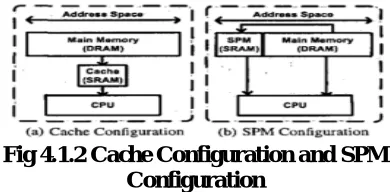
Scratchpad Memory Scratchpad Memory (SPM) is the term chosen for cache-like software-managed memory. It is significantly smaller than the main memory, ranging from below 1-KB to several KB in research applications and being at 256-KB in the SPEs of the Cell multiprocessor. Being located on the same chip as - and close to - the CPU core, its access latencies are negligible compared to those of the main memory. Unlike caches, SPM is not transparent to software. It is mapped into an address range different from the external RAM.
Fig 4.1.2 Cache Configuration and SPM Configuration
Some implementations make it possible for the CPU to continue its calculations while
data is transferred from RAM to SPM or vice versa by employing an asynchronous DMA controller. Even without it being asynchronous, transfers from or to RAM are often handled by a special controller that moves data in blocks rather than having the CPU using load and store instructions. There are approaches that use both a SPM and a regular cache.
In multicore processors, there may be a separate SPM per core, which can, depending on the implementation, be used as private buffer memory, ease communication between cores or both
Modern computer applications require more RAM to perform tasks than can be embedded into the processor core. Apart from some low-power embedded systems, most processors utilize cache hierarchies to lessen the speed penalty caused by access to external memory. Cache is a small temporary buffer managed by hardware, employing usually hard-wired displacement strategies like least-recently-used (LRU), first-in-first-out (FIFO) or randomized approaches. Since these displacement strategies are written to perform good for a wide spectrum of use cases, they are less optimal than a strategy that is tailored to a specific application by a compiler that knows about the whole program structure and may even employ profiling data.
4.2 Energy Efficiency
The main advantage of cache over SPM is that it is transparent to software. To achieve this, it needs to know which memory addresses lie within blocks that are currently stored in the cache. Tags are the parts of memory addresses that are required to map a block of cache memory to the address in the RAM it belongs to.
major part in the energy consumption of a modern processor, requiring from 25% to 45%, increasing its efficiency or replacing it with SPM has a significant impact on the energy consumption of the whole processor. To compare the energy and area efficiency of SPM and cache, modifies an existing processor, the ARM7TDMI, to use an SPM instead of the previously built-in cache. They employ the energy-away compiler with the post pass option of assigning code and data blocks with the knapsack algorithm.
4.3 Tag-SPM Architecture
The cache organization considered in this paper is a reconfigurable cache, which allows part of its cache ways to be configured as an SPM. The SPM consists of two portions: Data-SPM and Tag-SPM. The Data-SPM, which can be found in many commercial processors resides in the data RAM of the cache ways, which are configured as the SPM. On the other hand, the Tag-SPM resides in the tag RAM of the cache ways, which is our innovation. For completeness, we will begin with a description of the complete cache organization and operations, including both Data-SPM and Tag-SPM, and then focus on the proposed Tag-SPM technique.The proposed Tag-SPM technique can be applied to both the instruction cache and the data cache. To simplify the discussion, we use the data cache as the example in this paper.
.
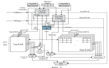
Fig 4.3 Tag-SPM architecture (4-kB, four-way associative cache, line size32 B).
6) The cache-SPM partitioning is way-based. That is, the programmer can set aside one or more ways to serve as the SPM while the remaining ways as the regular cache. When a way is configured as an SPM, both its tag RAM and data RAM are used to store data.
Support Circuitry for Tag-SPM and Data-SPM
The shaded components in provide the necessary mechanism to write data to tag RAM and data RAM and to read data from them. These components are three control registers (Tag-SPM base register, Data-SPM base register, and SPM way register), two controllers (Tag-SPM controller and Data-SPM controller), and four multiplexers (M1, M2, M3, and M4).
The programmer configures the Tag-SPM and Data-Tag-SPM regions by writing their starting addresses to Tag-SPM base register and Data-SPM base register, respectively. On the other hand, the SPM way register has n bits for an n-way cache. In our example, n is four. The programmer configures a cache way to function as an SPM by writing a logical value 1 to its corresponding bit. For instance, 0011 indicates that two cache ways, way1 and way0, are configured as SPMs, respectively. The multiplexers (M1–M4) select appropriate information for SPM-related components as follows.
1) M1 selects the Tag-SPM index or the Data-SPM index to address a line in the tag RAM and a line in the data RAM. When neither Tag-SPM nor Data-SPM is hit, the regular cache index (addr[9-5]) is passed from Tag-SPM controller to M1.
2) When in the Tag-SPM mode, the tag-SPM way selector M2 selects the line, as the Tag-SPM mode’s output, addressed by index in the tag RAM of the way designated by addr[8-7].
of Data RAM. When Data-SPM is hit, the output of M3 is Data-SPM Way (as addr[11-10]); otherwise, it may be a regular cache operation, and M3’s output is the way that has a tag hit.
4) Finally, M4 selects data from the tag RAM or the data RAM. When in the Tag-SPM mode, data from the tag RAM are output; when in either the regular cache mode or the Data-SPM mode, data from the data RAM are output.
Here, we summarize the operations of SPM modes. In the Tag-SPM mode, the Tag-SPM Hit signal is set, and the read/write operations are as the following. 1) For a read operation, Tag-SPM controller sends the set index signal TS_Index to tag RAMs to read the corresponding lines, while M2 selects the line from the way designated by the way index signal addr[8-7]. The selected line passes through M4 and becomes the cache’s RData output.
2) For a write operation, Tag-SPM controller sends the set index signal TS_Index to tag RAMs and sends the data value from WData to the write ports of the tag RAMs. The data are written to the tag RAM specified by the way index signal addr[8-7].
In the SPM mode, the Data-SPM Hit signal is set, and the read/write operations are as the following.
1) For a read operation, Data-SPM controller sends the set index signal DS_Index to data RAMs to read the corresponding lines, while multiplexers M3 and Data Select select the line from the way designated by the way index signal addr[11-10]. The selected line passes through M4 and becomes the cache’s RData output. 2) For a write operation, Data-SPM controller sends the set index signal DS_Index to data RAMs and sends the data value from WData to the write ports of the data RAMs. The data are written to the data RAM specified by the way index signal addr[8-7].
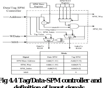
4.4. Tag/Data-SPM Controllers
Here, we elaborate the structure and operations of the Tag-SPM controller and the Data-SPM controller. Since their functionalities are similar, they share the same structure as in Fig. 4.4 where generic signal names are given without distinguishing Tag-SPM and Data-SPM modes.
The comparator matches the incoming memory address with the SPM Base register to see if the address falls within the SPM region. If the match happens in a way that is configured as an SPM as specified in the bits of the SPM Way register, the SPM_Hit signal is set. If the SPM is hit, multiplexers M5 and M6 output SPM_Index and WData, respectively. Otherwise, the index field and the tag field from the incoming address, interpreted according to the regular cache mode.
Fig 4.4 Tag/Data-SPM controller and definition of input signals.
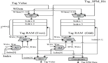
4.5. Special Consideration for Smaller Tag RAM Width
The bit width of the tag RAM of the cache in most modern processors is usually at least 32 bits, which can accommodate the typical 32-bit-wide memory data in the Tag-SPM mode. On the other hand, how can earlier processors such as Open RISC 1200, which has limited cache functionality and thus needs a narrower tag RAM (19-bit wide), accommodate the 32-bit memory data? One solution is to split the 32-bit data into two 16-bit sub data that each can be fitted into the narrower tag RAM. Therefore, it takes two accesses (cycles) to read/write 32-bit data. This solution is straightforward but slows down the memory operations. Here, we provide a better solution that utilizes the concept of banked RAMs to retain the single-cycle read/write latency in the Tag-SPM mode.
The organization of the even–odd tag RAM banks per way is shown in Fig. 4.5
Fig 4.5 Even–odd banked organization for a narrower tag RAM (16 ≤bitwidth ≤
31) (per way).
The shaded components, consisting of five multiplexers M7– M11 and two AND gates A1 and A2, are necessary to support the banked organization. Their operations are explained as the following.
1) Regular Cache Operations In the regular cache mode, the tag value is written to or read from the appropriate tag RAM bank. To write a tag value, M7 and M8 select the tag value as inputs to the tag RAM banks. M9, A1, M10, and A2 ensure that only one tag RAM bank is activated for
tag writing. On the other hand, to read a tag value, M11, controlled by the least significant bit of index, selects the proper tag RAM bank for output.
2) Tag-SPM Operations In the Tag-SPM mode (Tag_SPM_Hit being set), the data accessed are 32 bits wide and thus span an even bank and an odd bank. Therefore, both banks need to be activated. To write 32-bit data, M7 and M8, choose the upper and lower 16 bits of WData, respectively, and M9 and M10 ensure that both banks are enabled for writing. On the other hand, to perform a read, the concatenate logic at the bottom concatenates the two 16-bit data from the two banks into 32-bit data. With these arrangements, a 32-bit data read/write can be accomplished in one clock cycle.
E. Possible Critical Paths and Power Overhead
Because we add and modify hardware in the conventional cache, it is important to check if our Tag-SPM architecture has any impact on the circuit’s critical path. There are three possible paths that might be affected. First, the multiplexer M4 in Fig. 4.3 may add delay to the RData. Second, the two multiplexers in Fig. 4.4 might add delays to the data and index paths. Finally, when dealing with a tag RAM that is less than 32 bits wide, multiplexers M7, M8, and M11 in Fig. 4.5 might also add delays
INTRODUCTION TO VLSI
Very-large-scale integration (VLSI) is the process of creating integrated circuits by combining thousands of transistor-based circuits into a single chip. VLSI began in the 1970s when complex semiconductor and communication technologies were being developed. The microprocessor is a VLSI device. The term is no longer as common as it once was, as chips have increased in complexity into the hundreds of millions of transistors.
6.1 Overview
more and more transistors, and, as a consequence, more individual functions or systems were integrated over time. The first integrated circuits held only a few devices, perhaps as many as ten diodes, transistors, resistors and capacitors, making it possible to fabricate one or more logic gates on a single device. Now known retrospectively as "small-scale integration" (SSI), improvements in technique led to devices with hundreds of logic gates, known as large-scale integration (LSI), i.e. systems with at least a thousand logic gates. Current technology has moved far past this mark and today's microprocessors have many millions of gates and hundreds of millions of individual transistors.
At one time, there was an effort to name and calibrate various levels of large-scale integration above VLSI. Terms like Ultra-large-scale Integration (ULSI) were used. But the huge number of gates and transistors available on common devices has rendered such fine distinctions moot.
Terms suggesting greater than VLSI levels of integration are no longer in widespread use. Even VLSI is now somewhat quaint, given the common assumption that all microprocessors are VLSI or better.
As of early 2008, billion-transistor processors are commercially available, an example of which is Intel's Montecito Itanium chip. This is expected to become more commonplace as semiconductor fabrication moves from the current generation of 65 nm processes to the next 45 nm generations (while experiencing new challenges such as increased variation across process corners). Another notable example is NVIDIA’s 280 series GPU.
This microprocessor is unique in the fact that its 1.4 Billion transistor count, capable of a teraflop of performance, is almost entirely dedicated to logic (Itanium's transistor count is largely
due to the 24MB L3 cache). Current designs, as opposed to the earliest devices, use extensive design automation and automated logic synthesis to lay out the transistors, enabling higher levels of complexity in the resulting logic functionality. Certain high-performance logic blocks like the SRAM cell, however, are still designed by hand to ensure the highest efficiency (sometimes by bending or breaking established design rules to obtain the last bit of performance by trading stability).
Understanding why integrated circuit technology has such profound influence on the design of digital systems requires understanding both the technology of IC manufacturing and the economics of ICs and digital systems.
Applications
Electronic system in cars.
Digital electronics control VCRs
Transaction processing system, ATM
Personal computers and Workstations
Medical electronic systems.
Etc….
6.6 Applications of VLSI
Electronic systems now perform a wide variety of tasks in daily life. Electronic systems in some cases have replaced mechanisms that operated mechanically, hydraulically, or by other means; electronics are usually smaller, more flexible, and easier to service. In other cases electronic systems have created totally new applications. Electronic systems perform a variety of tasks, some of them visible, some more hidden:
Personal entertainment systems such as portable MP3 players and DVD players perform sophisticated algorithms with remarkably little energy.
perform the control functions required for anti-lock braking (ABS) systems.
Digital electronics compress and decompress video, even at high-definition data rates, on-the-fly in consumer electronics.
Low-cost terminals for Web browsing still require sophisticated electronics, despite their dedicated function.
Personal computers and workstations provide word-processing, financial analysis, and games. Computers include both central processing units (CPUs) and special-purpose hardware for disk access, faster screen display, etc.
Medical electronic systems measure bodily functions and perform complex processing algorithms to warn about unusual conditions. The availability of these complex systems, far from overwhelming consumers, only creates demand for even more complex systems.
ASIC
An Application-Specific Integrated Circuit (ASIC) is an integrated circuit (IC) customized for a particular use, rather than intended for general-purpose use. For example, a chip designed solely to run a cell phone is an ASIC. Intermediate between ASICs and industry standard integrated circuits, like the 7400 or the 4000 series, are application specific standard products (ASSPs).
As feature sizes have shrunk and design tools improved over the years, the maximum complexity (and hence functionality) possible in an ASIC has grown from 5,000 gates to over 100 million. Modern ASICs often include entire 32-bit processors, memory blocks including ROM, RAM, EEPROM, Flash and other large building blocks. Such an ASIC is often termed a SoC (system-on-a-chip). Designers of digital ASICs use a hardware description language (HDL), such as Verilog or VHDL, to describe the functionality of ASICs.
Field-programmable gate arrays (FPGA) are the modern-day technology for building a breadboard or prototype from standard parts; programmable logic blocks and programmable interconnects allow the same FPGA to be used in many different applications. For smaller designs and/or lower production volumes, FPGAs may be more cost effective than an ASIC design even in production.
An application-specific integrated circuit (ASIC) is an integrated circuit (IC) customized for a particular use, rather than intended for general-purpose use.
A Structured ASIC falls between an FPGA and a Standard Cell-based ASIC
Structured ASIC’s are used mainly for mid-volume level design. The design task for structured ASIC’s is to map the circuit into a fixed arrangement of known cells.
INTRODUCTION TO XILINX
Migrating Projects from Previous ISE Software Releases
When you open a project file from a previous release, the ISE® software prompts you to migrate your project. If you click Backup and Migrate or Migrate Only, the software automatically converts your project file to the current release. If you click Cancel, the software does not convert your project and, instead, opens Project Navigator with no project loaded.
Note: After you convert your project, you cannot open it in previous versions of the ISE software, such as the ISE 11 software. However, you can optionally create a backup of the original project as part of project migration, as described below.
To Migrate a Project
1. In the ISE 12 Project Navigator, select
File > Open Project.
2. In the Open Project dialog box, select the .xise file to migrate.
3. In the dialog box that appears, select
4. The ISE software automatically converts your project to an ISE 12 project.
5. Implement the design using the new version of the software.
Properties
For information on properties that have changed in the ISE 12 software, see ISE 11 to ISE 12 Properties Conversion.
IP Modules
If your design includes IP modules that were created using CORE Generator™ software or Xilinx® Platform Studio (XPS) and you need to modify these modules, you may be required to update the core. However, if the core netlist is present and you do not need to modify the core, updates are not required and the existing netlist is used during implementation.
Obsolete Source File Types
The ISE 12 software supports all of the source types that were supported in the ISE 11 software.
If you are working with projects from previous releases, state diagram source files (.dia), ABEL source files (.abl), and test bench waveform source files (.tbw) are no longer supported. For state diagram and ABEL source files, the software finds an associated HDL file and adds it to the project, if possible. For test bench waveform files, the software automatically converts the TBW file to an HDL test bench and adds it to the project. To convert a TBW file after project migration, see Converting a TBW File to an HDL Test Bench.
7.5 Using ISE Example Projects
To help familiarize you with the ISE® software and with FPGA and CPLD designs, a set of example designs is provided with Project Navigator. The examples show different design techniques and source types, such as VHDL, Verilog, schematic, or EDIF, and include different constraints and IP.
To Open an Example
Select File > Open Example.
In the Open Example dialog box, select the Sample Project Name.
In the Destination Directory field, enter a directory name or browse to the directory.
Click OK.
The example project is extracted to the directory you specified in the Destination Directory field and is automatically opened in Project Navigator. You can then run processes on the example project and save any changes.
Note If you modified an example project and want to overwrite it with the original example project, select File > Open Example, select the Sample Project Name, and specify the same Destination Directory you originally used. In the dialog box that appears, select Overwrite the existing project and click OK.
7.6 Creating a Project
Project Navigator allows you to manage your FPGA and CPLD designs using an ISE® project, which contains all the source files and settings specific to your design. First, you must create a project and then, add source files, and set process properties. After you create a project, you can run processes to implement, constrain, and analyze your design. Project Navigator provides a wizard to help you create a project as follows.
Note If you prefer, you can create a project using the New Project dialog box
instead of the New Project Wizard. To use the New Project dialog box, deselect the
Use New Project wizard option in the
ISE General page of the Preferences dialog box.
To Create a Project
1. Select File > New Project to launch the New Project Wizard.
2. In the Create New Project page, set the name, location, and project type, and click Next.
page, select the input and constraint file for the project, and click Next.
4. In the Project Settings page, set the device and project properties, and click
Next.
5. In the Project Summary page, review the information, and click Finish to create the project
Project Navigator creates the project file (project_name.xise) in the directory you specified. After you add source files to the project, the files appear in the Hierarchy pane of the
Design panel
Project Navigator manages your project based on the design properties (top-level module type, device type, synthesis tool, and language) you selected when you created the project. It organizes all the parts of your design and keeps track of the processes necessary to move the design from design entry through implementation to programming the targeted Xilinx® device.
Note For information on changing design properties, see Changing Design Properties.
You can now perform any of the following:
Create new source files for your project.
Add existing source files to your project.
Run processes on your source files.
Modify process properties.
7.8 Creating a Copy of a Project
You can create a copy of a project to experiment with different source options and implementations. Depending on your needs, the design source files for the copied project and their location can vary as follows:
Design source files are left in their existing location, and the copied project points to these files.
Design source files, including generated files, are copied and placed in a specified directory.
Design source files, excluding generated files, are copied and placed in a specified directory.
Copied projects are the same as other projects in both form and function. For example, you can do the following with copied projects:
Open the copied project using the File > Open Project menu command.
View, modify, and implement the copied project.
Use the Project Browser to view key summary data for the copied project and then, open the copied project for further analysis and implementation, as described in
Using the Project Browser
Alternatively, you can create an archive of your project, which puts all of the project contents into a ZIP file. Archived projects must be unzipped before being opened in Project Navigator. For information on archiving, see Creating a Project Archive.
To Create a Copy of a Project
1. Select File > Copy Project.
2. In the Copy Project dialog box, enter the
Name for the copy.
Note The name for the copy can be the same as the name for the project, as long as you specify a different location. 3. Enter a directory Location to store the
copied project.
4. Optionally, enter a Working directory. By default, this is blank, and the working directory is the same as the project directory. However, you can specify a working directory if you want to keep your ISE® project file (.xise extension) separate from your working area.
5. Optionally, enter a Description for the copy.
6. In the Source options area, do the following:
Select one of the following options:
Keep sources in their current
locations - to leave the design source files in their existing location.
If you select this option, the copied project points to the files in their existing location. If you edit the files in the copied project, the changes also appear in the original project, because the source files are shared between the two projects.
Copy sources to the new location - to make a copy of all the design source files and place them in the specified Location directory.
If you select this option, the copied project points to the files in the specified directory. If you edit the files in the copied project, the changes do not appear in the original project, because the source files are not shared between the two projects.
Optionally, select Copy files from Macro Search Path directories to copy files from the directories you specify in the Macro Search Path property in the
Translate Properties dialog box. All files from the specified directories are copied, not just the files used by the design.
Note: If you added a net list source file directly to the project as described in
Working with Net list-Based IP, the file is automatically copied as part of Copy Project because it is a project source file. Adding net list source files to the project is the preferred method for incorporating net list modules into your design, because the files are managed automatically by Project Navigator.
Optionally, click Copy Additional Files to copy files that were not included in the original project. In the Copy Additional Files dialog box, use the Add Files and
Remove Files buttons to update the list of additional files to copy. Additional files are copied to the copied project location after all other files are copied. To exclude
generated files from the copy, such as implementation results and reports, select
7.10 Exclude generated files from the copy
When you select this option, the copied project opens in a state in which processes have not yet been run.
7. To automatically open the copy after creating it, select Open the copied project.
Note By default, this option is disabled. If you leave this option disabled, the original project remains open after the copy is made.
Click OK.
Creating a Project Archive
A project archive is a single, compressed ZIP file with a .zip extension. By default, it contains all project files, source files, and generated files, including the following:
User-added sources and associated files
Remote sources
Verilog include files
Files in the macro search path
Generated files
Non-project files
To Archive a Project
1. Select Project > Archive.
2. In the Project Archive dialog box, specify a file name and directory for the ZIP file.
3. Optionally, select Exclude generated files from the archive to exclude generated files and non-project files from the archive.
4. Click OK.
A ZIP file is created in the specified directory. To open the archived project, you must first unzip the ZIP file, and then, you can open the project.
INTRODUCTION TO VERILOG
language), is most commonly used in the design, verification, and implementation of digital logic chips at the register-transfer level of abstraction. It is also used in the verification of analog and mixed-signal circuits.
SystemVerilog
SystemVerilog is a superset of Verilog-2005, with many new features and capabilities to aid design verification and design modeling. As of 2009, the SystemVerilog and Verilog language standards were merged into SystemVerilog 2009 (IEEE Standard 1800-2009).
The advent of hardware verification languages such as OpenVera, and Verisity's e language encouraged the development of Superlog by Co-Design Automation Inc. Co-Design Automation Inc was later purchased by Synopsys. The foundations of Superlog and Vera were donated to Accellera, which later became the IEEE standard P1800-2005: SystemVerilog.
In the late 1990s, the Verilog Hardware Description Language (HDL) became the most widely used language for describing hardware for simulation and synthesis. However, the first two versions standardized by the IEEE (1364-1995 and 1364-2001) had only simple constructs for creating tests. As design sizes outgrew the verification capabilities of the language, commercial Hardware Verification Languages (HVL) such as Open Vera and were created. Companies that did not want to pay for these tools instead spent hundreds of man-years creating their own custom tools. The donation of the Open-Vera language formed the basis for the HVL features of SystemVerilog. Accellera’s goal was met in November 2005 with the adoption of the IEEE standard P1800-2005 for SystemVerilog, IEEE (2005).
Some of the typical features of an HVL that distinguish it from a Hardware Description Language such as Verilog or VHDL are
Constrained-random stimulus generation
Functional coverage
Higher-level structures, especially Object Oriented Programming
Multi-threading and inter process communication
Support for HDL types such as Verilog’s 4-state values
Tight integration with event-simulator for control of the design
There are many other useful features, but these allow you to create test benches at a higher level of abstraction than you are able to achieve with an HDL or a programming language such as C.
System Verilog provides the best framework to achieve coverage-driven verification (CDV). CDV combines automatic test generation, self-checking testbenches, and coverage metrics to significantly reduce the time spent verifying a design.
The purpose of CDV is to
Eliminate the effort and time spent creating hundreds of tests.
Ensure thorough verification using up-front goal setting.
Receive early error notifications and deploy run-time checking and error analysis to simplify debugging.
Examples
Ex1 A hello world program looks like this:
module main; initial
begin
$display("Hello world!"); $finish;
end
endmodule
would not have been swapped. Instead, as in traditional programming, the compiler would understand to simply set flop1 equal to flop2 (and subsequently ignore the redundant logic to set flop2 equal to flop1.)
Ex3 An example counter circuit follows
module Div20x (rst, clk, cet, cep, count, tc); // TITLE 'Divide-by-20 Counter with enables'
// enable CEP is a clock enable only // enable CET is a clock enable and // enables the TC output
// a counter using the Verilog language parameter size = 5;
parameter length = 20;
input rst; // These inputs/outputs represent input clk; // connections to the module. input cet;
input cep;
output [size-1:0] count; output tc;
reg [size-1:0] count; // Signals assigned // within an always
// (or initial)block // must be of type reg
wire tc; // Other signals are of type wire // The always statement below is a parallel // execution statement that
// executes any time the signals // rst or clk transition from low to high always @ (posedge clk or posedge rst) if (rst) // This causes reset of the cntr count <= {size{1'b0}};
else
if (cet && cep) // Enables both true begin
if (count == length-1) count <= {size{1'b0}}; else
count <= count + 1'b1; end
// the value of tc is continuously assigned // the value of the expression
assign tc = (cet && (count == length-1)); endmodule
The always clause above illustrates the other type of method of use, i.e. the always clause executes any time any of the entities in the list change, i.e. the b or e change. When one of these changes, immediately a is assigned a new value, and due to the blocking assignment b is assigned a new value afterward (taking into account the new value of a.) After a delay of 5 time units, c is assigned the value of b and the value of c ^ e is tucked away in an invisible store. Then after 6 more time units, d is assigned the value that was tucked away.
Signals that are driven from within a process (an initial or always block) must be of type reg. Signals that are driven from outside a process must be of type wire. The keyword reg does not necessarily imply a hardware register.
Constants
The definition of constants in Verilog supports the addition of a width parameter. The basic syntax is:
<Width in bits>'<base letter><number> Examples:
12'h123 - Hexadecimal 123 (using 12 bits)
20'd44 - Decimal 44 (using 20 bits - 0 extension is automatic)
4'b1010 - Binary 1010 (using 4 bits)
6'o77 - Octal 77 (using 6 bits)
8.4 Synthesizable Constructs
There are several statements in Verilog that have no analog in real hardware, e.g. $display. Consequently, much of the language can not be used to describe hardware. The examples presented here are the classic subset of the language that has a direct mapping to real gates.
// Mux examples - Three ways to do the same thing.
// The first example uses continuous assignment
wire out;
// the second example uses a procedure // to accomplish the same thing. reg out;
always @(a or b or sel) begin
case(sel) 1'b0: out = b; 1'b1: out = a; endcase end
// Finally - you can use if/else in a // procedural structure.
reg out;
always @(a or b or sel) if (sel)
out = a; else out = b;
The next interesting structure is a transparent latch; it will pass the input to the output when the gate signal is set for "pass-through", and captures the input and stores it upon transition of the gate signal to "hold". The output will remain stable regardless of the input signal while the gate is set to "hold". In the example below the "pass-through" level of the gate would be when the value of the if clause is true, i.e. gate = 1. This is read "if gate is true, the din is fed to latch_out continuously." Once the if clause is false, the last value at latch_out will remain and is independent of the value of din.
EX6: // Transparent latch example reg out;
always @(gate or din) if(gate)
out = din; // Pass through state
// Note that the else isn't required here. The variable
// out will follow the value of din while gate is high.
// When gate goes low, out will remain constant.
The flip-flop is the next significant template; in Verilog, the D-flop is the simplest, and it can be modeled as:
reg q;
always @(posedge clk) q <= d;
The significant thing to notice in the example is the use of the non-blocking assignment. A basic rule of thumb is to
use <= when there is a
posedge or negedge statement within the always clause.
A variant of the D-flop is one with an asynchronous reset; there is a convention that the reset state will be the first if clause within the statement.
reg q;
always @(posedge clk or posedge reset) if(reset)
q <= 0; else q <= d;
The next variant is including both an asynchronous reset and asynchronous set condition; again the convention comes into play, i.e. the reset term is followed by the set term.
reg q;
always @(posedge clk or posedge reset or posedge set)
if(reset) q <= 0; else if(set) q <= 1; else q <= d;
Note that there are no "initial" blocks mentioned in this description. There is a split between FPGA and ASIC synthesis tools on this structure. FPGA tools allow initial blocks where reg values are established instead of using a "reset" signal. ASIC synthesis tools don't support such a statement. The reason is that an FPGA's initial state is something that is downloaded into the memory tables of the FPGA. An ASIC is an actual hardware implementation.
8.5 Initial Vs Always
There are two separate ways of declaring a Verilog process. These are the always and the initial keywords. The always keyword indicates a free-running process. The initial keyword indicates a process executes exactly once. Both constructs begin execution at simulator time 0, and both execute until the end of the block. Once an always block has reached its end, it is rescheduled (again). It is a common misconception to believe that an initial block will execute before an always block. In fact, it is better to think of the initial-block as a special-case of the always-block, one which terminates after it completes for the first time.
//Examples: initial begin
a = 1; // Assign a value to reg a at time 0 #1; // Wait 1 time unit
b = a; // Assign the value of reg a to reg b end
always @(a or b) // Any time a or b CHANGE, run the process
begin if (a) c = b; else d = ~b;
end // Done with this block, now return to the top (i.e. the @ event-control)
always @(posedge a)// Run whenever reg a has a low to high change
a <= b;
These are the classic uses for these two keywords, but there are two significant additional uses. The most common of these
is an alwayskeyword without
the @(...) sensitivity list. It is possible to use always as shown below:
always
begin // Always begins executing at time 0 and NEVER stops
clk = 0; // Set clk to 0 #1; // Wait for 1 time unit clk = 1; // Set clk to 1 #1; // Wait 1 time unit
end // Keeps executing - so continue back at the top of the begin
The always keyword acts similar to the "C" construct while(1) {..} in the sense that it will execute forever.
The other interesting exception is the use of the initial keyword with the addition of the forever keyword.
Race Condition
The order of execution isn't always guaranteed within Verilog. This can best be illustrated by a classic example. Consider the code snippet below:
initial a = 0; initial b = a; initial begin #1;
$display("Value a=%b Value of b=%b",a,b);
end
assignment blocks have completed, due to the #1 delay.
System Tasks
System tasks are available to handle simple I/O, and various design measurement functions. All system tasks are prefixed with $ to distinguish them from user tasks and functions. This section presents a short list of the most often used tasks. It is by no means a comprehensive list.
$display - Print to screen a line followed by an automatic newline.
$write - Write to screen a line without the newline.
$swrite - Print to variable a line without the newline.
$sscanf - Read from variable a format-specified string. (*Verilog-2001)
$fopen - Open a handle to a file (read or write)
$fdisplay - Write to file a line followed by an automatic newline.
$fwrite - Write to file a line without the newline.
$fscanf - Read from file a format-specified string. (*Verilog-2001)
$fclose - Close and release an open file handle.
$readmemh - Read hex file content into a memory array.
$readmemb - Read binary file content into a memory array.
$monitor - Print out all the listed variables when any change value.
$time - Value of current simulation time.
$dumpfile - Declare the VCD (Value Change Dump) format output file name.
$dumpvars - Turn on and dump the variables.
$dumpports - Turn on and dump the
variables in Extended-VCD format. CONCLUSION
In this project presented the Tag-SPM architecture, which allows the tag RAM to be used as the SPM and thus increases the SPM capacity. It is accomplished with small
Tag/Data- SPM controllers and four additional multiplexers in the cache organization. We also provide an even–odd banked solution for some early processors with simpler caches. The proposed Tag-SPM architecture has been implemented with an academic ARM-based microprocessor with a 4-kB four-way instruction cache and a 4-kB four-way data cache at RTL level.
REFERENCES
[1] Cortex-A5 Technical Reference Manual, ARM Ltd., Cambridge, U.K., Sep. 2010.
[2] ARM Cortex-A53 Technical Reference Manual, ARM Ltd., Cambridge,U.K., Feb.2014.
[3] O. Avissar, R. Barua, and D. Stewart, “An optimal memory allocation scheme for scratch-pad-based embedded systems,” ACM Trans. Embedded Comput. Syst., vol. 1, no.1, pp. 6–26, 2002.
[4] R. Banakar, S. Steinke, B.-S. Lee, M. Balakrishnan, and P. Marwedel,“Scratchpad memory: Design alternative for cache on-chip memory in embedded systems,” in Proc. 10th Int. Symp. Hardw./Softw. Codesign, 2002, pp. 73–78.
[5] L. Benini, A. Macii, E. Macii, and M. Poncino, “Increasing energy efficiency of embedded systems by application-specific memory hierarchy generation,” IEEE Design Test Comput., vol. 17, no. 2, pp. 74–85, Apr. 2000.
[6] N. Binkert et al., “The gem5 simulator,” ACM SIGARCH Comput. Archit. News, vol. 39, no. 2, pp. 1–7, 2011. [7] Y.-T. Chen et al., “Dynamically
reconfigurable hybrid cache: An energy-efficient last-level cache design,” in Proc. Design, Autom. Test Eur. Conf. Exhibit. (DATE), Mar. 2012, pp. 45–50.
energy-efficient adaptive hybrid cache,” in Proc. Int. Symp. Low Power Electron. Design, Aug. 2011, pp.67–72.
[9] H. Cook, K. Asanovi´c, and D. A. Patterson, “Virtual local stores: Enabling software-managed memory hierarchies in mainstream computing environments,” Univ. California,Berkeley, Berkeley, CA, USA, Tech. Rep. UCB/EECS-2009-131, 2009.
[10] J. Edler. (1998). Dinero IV Trace-Driven Uniprocessor Cache Simulator. [Online]. Available: http://www.cs.wisc.edu/~markhill/Dine roIV/ [11] Gaisler Research. LEON2 Cache Memory VHDL Code. Accessed: Dec. 31, 2017. [Online]. Available:
https://github.com/Galland/LEON2/
blob/master/leon2-1.0.30-xst/leon/cachemem.vhd
[12] Z. Ge, W.-F. Wong, and H.-B. Lim, “DRIM: A low power dynamically reconfigurable instruction memory hierarchy for embedded systems,” in Proc. Design, Autom. Test Eur. Conf. Exhibit., Apr. 2007, pp. 1–6.
[13] M. R. Guthaus, J. S. Ringenberg, D. Ernst, T. M. Austin, T. Mudge,and R. B. Brown, “MiBench: A free, commercially representative embedded benchmark suite,” in Proc. IEEE Int. Workshop Workload Characterization (WWC), Dec. 2001, pp. 3–14.
[14] Texas Instruments. TMS320C6000 Programmers Guide. Accessed: Dec. 31, 2017. [Online]. Available: http://www.ti.com/lit/ug/spru198k/ spru198k.pdf.
[15] Intel. 3rd Generation Intel XScale Microarchitecture. Accessed: Dec. 31, 2017. [Online]. Available: http://download.intel.com/design/ intelxscale/31628302.pdf.
[16] G. Kalokerinos et al., “Prototyping a configurable cache/scratchpad memory with virtualized user-level RDMA
capability,” Trans. High Perform. Embedded Archit. Compilation, vol. 5, no. 3, pp. 75–95,Aug. 2010.
[17] M. Kandemir, J. Ramanujam, M. J. Irwin, N. Vijaykrishnan, I. Kadayif, and A. Parikh, “Dynamic management of scratch-pad memory space,”in Proc. Design Autom. Conf., 2001, pp. 690– 695.
[18] T. Kluter, P. Brisk, P. Ienne, and E. Charbon, “Way stealing: Cacheassisted automatic instruction set extensions,” in Proc. ACM/IEEE Design Autom. Conf., Jul. 2009,
pp. 31-36.
[19] D. Lampret. OpenRISC 1200 Tag RAM of the Data Cache Source Code. Accessed: Dec. 31, 2017. [Online]. Available:
https://github.com/openrisc/or1200/blo b/master/rtl/verilog/or1200_dc_tag.v [20] C. Lim and G. T. Byrd, “Exploiting
producer patterns and L2 cache for timely dependence-based prefetching,” in Proc. IEEE Int. Conf. Comput. Design, Oct. 2008, pp.685–692.
[21] NVIDIA. NVIDIA’s Next Generation CUDA Compute Architecture: Fermi. Accessed: 2009. [Online].
Available:http://www.nvidia.com/conte nt/PDF/fermi_white_papersNVIDIA_F ermi_Compute_Architecture_Whitepap er.pdf
[22] I. Puaut and C. Pais, “Scratchpad memories vs locked caches in hard real-time systems: A quantitative comparison,” in Proc. Design, Autom. Test Eur. Conf. Exhibit. (DATE), Apr. 2007, pp. 1–6.