University of Windsor University of Windsor
Scholarship at UWindsor
Scholarship at UWindsor
Electronic Theses and Dissertations Theses, Dissertations, and Major Papers
2008
Investigation of an Atomic Force Microscope (AFM) probe under
Investigation of an Atomic Force Microscope (AFM) probe under
electrostatic actuation
electrostatic actuation
Liton Ghosh
University of Windsor
Follow this and additional works at: https://scholar.uwindsor.ca/etd
Recommended Citation Recommended Citation
Ghosh, Liton, "Investigation of an Atomic Force Microscope (AFM) probe under electrostatic actuation" (2008). Electronic Theses and Dissertations. 7884.
https://scholar.uwindsor.ca/etd/7884
This online database contains the full-text of PhD dissertations and Masters’ theses of University of Windsor students from 1954 forward. These documents are made available for personal study and research purposes only, in accordance with the Canadian Copyright Act and the Creative Commons license—CC BY-NC-ND (Attribution, Non-Commercial, No Derivative Works). Under this license, works must always be attributed to the copyright holder (original author), cannot be used for any commercial purposes, and may not be altered. Any other use would require the permission of the copyright holder. Students may inquire about withdrawing their dissertation and/or thesis from this database. For additional inquiries, please contact the repository administrator via email
Investigation of an
Atomic Force Microscope (AFM)
Probe under Electrostatic Actuation
by
Liton Ghosh
A Thesis
Submitted to the Faculty of Graduate Studies through Electrical Engineering
in Partial Fulfillment of the Requirements for the Degree of Master of Applied Science at the
University of Windsor
Windsor, Ontario, Canada
2008
1*1
Library and Archives CanadaPublished Heritage Branch
395 Wellington Street Ottawa ON K1A0N4 Canada
Bibliotheque et Archives Canada
Direction du
Patrimoine de I'edition
395, rue Wellington Ottawa ON K1A0N4 Canada
Your file Votre reference ISBN: 978-0-494-47087-9 Our file Notre reference ISBN: 978-0-494-47087-9
NOTICE:
The author has granted a non-exclusive license allowing Library and Archives Canada to reproduce, publish, archive, preserve, conserve, communicate to the public by
telecommunication or on the Internet, loan, distribute and sell theses
worldwide, for commercial or non-commercial purposes, in microform, paper, electronic and/or any other formats.
AVIS:
L'auteur a accorde une licence non exclusive permettant a la Bibliotheque et Archives Canada de reproduire, publier, archiver,
sauvegarder, conserver, transmettre au public par telecommunication ou par I'lnternet, prefer, distribuer et vendre des theses partout dans le monde, a des fins commerciales ou autres, sur support microforme, papier, electronique et/ou autres formats.
The author retains copyright ownership and moral rights in this thesis. Neither the thesis nor substantial extracts from it may be printed or otherwise reproduced without the author's permission.
L'auteur conserve la propriete du droit d'auteur et des droits moraux qui protege cette these. Ni la these ni des extraits substantiels de celle-ci ne doivent etre imprimes ou autrement reproduits sans son autorisation.
In compliance with the Canadian Privacy Act some supporting forms may have been removed from this thesis.
While these forms may be included in the document page count,
their removal does not represent any loss of content from the thesis.
• * •
Canada
Conformement a la loi canadienne sur la protection de la vie privee, quelques formulaires secondaires ont ete enleves de cette these.
AUTHOR'S DECLARATION OF ORIGINALITY
I hereby certify that I am the sole author of this thesis and that no part of this thesis has
been published or submitted for publication.
I certify that, to the best of my knowledge, my thesis does not infringe upon anyone's
copyright nor violate any proprietary rights and that any ideas, techniques, quotations, or
any other material from the work of other people included in my thesis, published or
otherwise, are fully acknowledged in accordance with the standard referencing practices.
Furthermore, to the extent that I have included copyrighted material that surpasses the
bounds of fair dealing within the meaning of the Canada Copyright Act, I certify that I
have obtained a written permission from the copyright owner(s) to include such
material(s) in my thesis and have included copies of such copyright clearances to my
appendix.
I declare that this is a true copy of my thesis, including any final revisions, as approved
by my thesis committee and the Graduate Studies office, and that this thesis has not been
ABSTRACT
This thesis develops a readily computable closed-form analytical model to determine the
pull-in voltage of an Atomic Force Microscope (AFM) probe under electrostatic
actuation. The analytical model has been derived based on the Euler-Bernoulli beam
theory, Taylor series expansion of the electrostatic energy stored in the AFM probe, and
deflection function of the first natural mode of a cantilever beam. The model takes
account of the electrostatic energy associated with the fringing field capacitances
between the AFM probe cantilever and the substrate to develop a more accurate model of
the stored electrostatic energy after the system is biased with a DC voltage. The
developed energy model is then used to develop a highly accurate closed-form model for
the pull-in voltage of the AFM probe. The developed closed-form model has been
verified by comparing the model predicted values with published experimental results
with a maximum deviation of 3.36%. The model has also been compared with a
published curve model and 3-D electromechanical finite element analysis (FEA) results.
ACKNOWLEDGEMENTS
I want to take the opportunity to acknowledge the people without whom this work would
not have been possible. Firstly I want to express my sincere gratitude to my thesis
supervisor, Dr. Sazzadur Chowdhury, for giving me the opportunity to work in the field
of MEMS and Atomic Force Microscope, for his expert guidance and financial support,
as well as for accepting topic of my thesis.
I would like to thank the Natural Sciences and Engineering Research Council of Canada
(NSERC) and Ontario Centers of Excellence for supporting my research. I would like to
thank the additional generous support provided by the Canadian Microelectronics
Corporation (CMC), and the IntelliSense Software Corporation of Woburn, MA. I want
to extend a very special thank to John Bloomsburgh of IntelliSense Software Corporation
for helping me in carrying out the finite element analysis.
Thanks to Dr. Roberto Muscedere for arranging me a high performance machine in
Research Center for Integrated Microsystems (RCIM) lab for running simulations for my
project and also for the helps he did to me whenever I had any problem with those
machines.
I would like to express my deepest gratitude to friends and co-workers who shaped the
warm environment at University of Windsor. Special thanks to Jose Martinez-Quijada for
helping me out with IntelliSuite and for his brother like motivation. I would like to give a
big thank to my friend, Peng Chang's for his moral supports and inspirations.
The greatest acknowledgement to my mother, Tulshi Ghosh, to my father, Bimal Ghosh
and to my brother, Dipon Ghosh, whose love has accompanied me far away from
Bangladesh, from where their efforts brought reality to my dream of completing the
degree of Master of Applied Science in Canada, giving me unconditional and generous
support that allowed me to live without lacking anything. A special thanks to my mother
TABLE OF CONTENTS
AUTHOR'S DECLARATION OF ORIGINALITY iii
ABSTRACT iv
DEDICATION v
ACKNOWLEDGEMENTS vi
LIST OF TABLES xi
LIST OF FIGURES xii
LIST OF APPENDICES xiv
CHAPTER 1: INTRODUCTION 1
1.1 Goals 1
1.2 Background 2
1.2.1 Atomic Force Microscope Fundamentals 2
1.2.2 State of the Art in Pull-in Voltage modeling of an AFM Probe 6
1.2.3 Limitations of Existing Models 9
1.3 Scientific Approach to Solve the Problem 10
1.4 Principal Results 10
1.5 Organization of Thesis 11
CHAPTER 2: DEVICE MODELING CONSIDERATIONS 13
2.1 Geometry of an Atomic Force Microscope probe 13
2.2 Energy of AFM Probe-Substrate System 15
2.2.2 Electrostatic Energy 16
2.2.3 Van der Waals Energy 17
CHAPTER 3: ELECTROSTATIC ENERGY MODELING 19
3.1 Capacitance Associated with AFM Probe cantilever 19
3.2 Capacitance Associated with AFM Tip Cone 23
3.3 Capacitance Associated with AFM Tip Apex 23
3.4 Electrostatic Energy of AFM Probe-Substrate System 24
CHAPTER 4: PULL-IN VOLTAGE MODELING 25
4.1 Total Energy of AFM Probe-Substrate System 25
4.2 Pull-in Voltage Closed-Form Model 29
CHAPTER 5: FEA MODELING 35
5.1 Construction of Atomic Force Microscope Probes 35
5.1.1 Geometry of First Probe 36
5.1.2 Geometry of Second Probe 39
5.2 Meshing of Atomic Force Microscope Probes 42
5.2.1 Meshing of the Probes 44
CHAPTER 6: MODEL VERIFICATION 50
6.1 Comparison with Experimentally Determined Values and Values Determined
from a Published Model 50
6.2 Comparison with Finite Element Analysis (FEA) Results 54
CONCLUSION 63
REFERENCES 66
APPENDIX B 80
LIST OF TABLES
Table 1. Specifications of AFM probes 36
Table 2. AFM probe Material properties (AFM probe 1) 51
Table 3. Pull-in Voltage Comparison for Different Methods (AFM probe 1) 51
Table 4. Pull-in Voltage comparison (AFM probe 1) 52
Table 5. Pull-in Voltage from FEA (AFM probe 1) 59
Table 6. Pull-in Voltage from FEA (AFM probe 2) 59
Table 7. Pull-in Voltage Comparison with FEA and New Model (AFM probe 1) 60
LIST OF FIGURES
Figure 1. Block Diagram of Atomic Force Microscope System 3
Figure 2. Close up Views of Atomic Force Microscope probe, (a-d) SEM images of an
AFM probe (Courtesy: Nanosensors) and (e-f) different parts of AFM probe 5
Figure 3. Microfabricated cantilever beam [13]. (a) Before pull-in, (b) After pull-in 6
Figure 4. A curled beam [14] 6
Figure 5. A schematic diagram of the AFM probe model used in [12] showing parameter
notations 7
Figure 6. A schematic diagram of AFM probe-substrate system showing the cantilever
length L, width w, thickness ^ and the height of the cone H 14
Figure 7. A line diagram of the AFM probe showing the radius R of the spherical apex
of the cone, half opening angel 6 of the cone, and the inclination angel Piever of the
cantilever with respect to substrate plane 14
Figure 8. A schematic diagram of AFM probe-substrate system showing different forces
acting on AFM probe 15
Figure 9. A schematic diagram of the AFM probe-substrate system showing various
capacitance components 17
Figure 10. Schematic diagram of AFM probe cantilever arrangement 20
Figure 11. Geometry of AFM probe 1. (a) Front view of whole of the AFM
probe-substrate system, (b) Side view of the AFM probe, (c) Orthogonal view of the AFM
probe, (d) Side view of the pyramidal tip cone and the part of cantilever, (e) Spherical tip
apex at the end of the tip 39
Figure 12. Geometry of AFM probe 2. (a) Front view of whole of the AFM
probe-substrate system, (b) Side view of the AFM probe, (c) Orthogonal view of the AFM
probe, (d) Side view of the pyramidal tip cone and the part of cantilever, (e) Spherical tip
apex at the end of the tip 42
Figure 13. Different mesh sizes for different part of AFM probe 1. (a) Front view of the
meshing of the AFM probe and the substrate, (b) Side view of the meshing of the
pyramidal tip cone and the substrate, (c) Front view of the meshing of the tip apex, (d)
Figure 14. Different mesh sizes for different part of AFM probe 2. (a) Front view of the
meshing of the AFM probe and the substrate, (b) Side view of the meshing of the
pyramidal tip cone and the substrate, (c) Front view of the meshing of the tip apex, (d)
Side view of the meshing of tip apex 48
Figure 15. Pull-in voltage comparison of new closed-form model and published curve
model in [12] 53
Figure 16. Initial distance vs. Pull-in voltage curve redrawn from [12] 54
Figure 17. Pull-in of the spherical tip apex of AFM probe lonto the substrate, (a) Front
view (b) Side view 55
Figure 18. Pull-in of the spherical tip apex of AFM probe 2 onto the substrate, (a) Front
view (b) Side view 56
Figure 19. Visualization of the displacement of different parts of AFM probe 1 in a color
scale 57
Figure 20. Visualization of the displacement of different parts of AFM probe 2 in a color
LIST OF APPENDICES
APPENDIX A: MATLAB SCRIPTS 70
CHAPTER 1
INTRODUCTION
1.1 Goals
With the recent growth of the use of Atomic Force Microscopy (AFM) for surface
characterization, nanoscale feature extraction, and nanoparticle manipulation, there is a
need for a readily computable but accurate closed-form analytical model to determine the
pull-in voltage of an AFM probe under electrostatic actuation. If the applied bias voltage
is equal or greater than a certain limit called the pull-in voltage, the probe collapses on
the substrate (surface under investigation) due to an electrostatic attraction force between
the deformable probe and the fixed substrate. In order to avoid this pull-in problem,
knowledge of load-deflection characteristic and accurate determination of the pull-in
voltage is critical for proper operation of an AFM probe. The overall goal of this thesis is
to develop, demonstrate and validate a readily computable closed-form model to
determine the pull-in voltage of an AFM probe under electrostatic actuation.
Based on this objective, the specific goals of this research work have been set as follows:
1. Develop a highly accurate analytical model for the electrostatic energy in
Atomic Force Microscope (AFM) probe-substrate system.
2. Use the developed energy model to develop a readily computable highly
accurate closed-form analytical model for the pull-in voltage of an Atomic
Force Microscope probe and provide load-deflection characteristic of an
3. Verify the accuracy of the developed closed-form pull-in voltage model by
comparing the model predicted values with results from experimental, 3-D
electromechanical Finite Element Analysis (FEA), and results from other
published models.
1.2 Background
1.2.1 Atomic Force Microscope Fundamentals
Atomic Force Microscope was first invented by Binnig [1]. AFM is a type of Scanning
Probe Microscope with sub-nanometer scale resolutions. Scanning Tunneling Microscope
(STM) has the ability to resolve atomic structure of a sample but it can only be applied to
conducive or semi-conductive specimens. To extend the technique to a wider variety of
materials including insulators, AFM was developed in 1986. AFM operates under
ambient or near ambient condition and can even be used in a liquid environment. AFM
can be used on a wide variety of surface types, ranging from hard and crystalline to soft
and pliable, even living entities like cell specimens.
Primarily AFM probe has been extensively used to image the surface of any sample.
Later on it's use has been extended to obtain information about surface properties such as
local surface potentials [2], surface charges [3-4], surface polarization forces [5],
magnetic properties of surfaces [6]. However, in recent years, AFM has been identified as
a powerful nanolithography tool [7-8] and some researchers demonstrated that AFM can
be used to manipulate nanoparticles [9-12]. In [9-11] electrical manipulation of
nanoparticles with AFM using AC voltages were demonstrated. In [12] DC voltage was
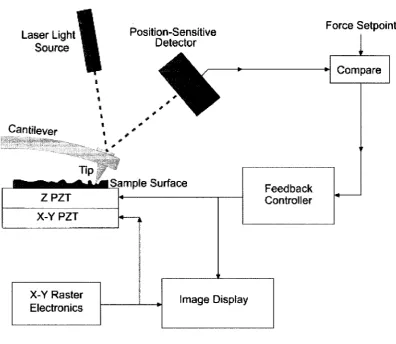
Figure 1 shows the basic components and working principles of an AFM system.
Laser Light Source
Position-Sensitive Detector
Cantilever » #
Force Setpoint
I
Compare
Tip; ZPZT X-Y PZT
X-Y Raster Electronics
Sample Surface Feedback Controller
Image Display
An Atomic Force Microscope is constructed using
• Piezoelectric Materials
• Feedback Control
• Force Sensors
In the system, a microfabricated cantilever with a sharp tip at the end is used as a force
sensor which is called the AFM probe. When the tip is brought closer to the surface, the
forces between the tip and the sample cause the cantilever to bend. This motion is
detected optically by the deflection of a laser beam (typically 635 nm Ar laser) which is
reflected off the back of the cantilever. This detected signal is compared and then fed to
feedback controller. The feedback controller keeps the force constant by controlling the
expansion of the Z piezoelectric transducer. The X-Y piezoelectric ceramics are used to
scan the probe across the surface in a raster-like pattern. By monitoring the voltage on the
Z piezoelectric transducer, an image of the surface is obtained.
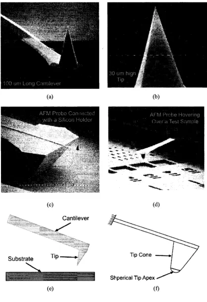
Figure 2 (a-d) shows Scanning Electron Microscope (SEM) images of a real AFM probe.
Figure 2 (e-f) shows the conceptual line diagram of an AFM probe. An AFM probe can
be divided into 3 parts.
• Cantilever
• Tip Cone
(a) (b)
(c)
Cantilever
Substrate T , p
^
(e)
(d)
Shperical Tip Apex
(f)
Figure 2. Close up Views of Atomic Force Microscope probe, (a-d) SEM images of an
1.2.2 State of the Art in Pull-in Voltage modeling of an AFM Probe
There has been very little published work available in the public domain that pursued to
develop some closed-form readily usable analytical method to determine the pull-in
voltage and the pull-in distance associated with an AFM probe. There are existing models
for the electrostatic bending of cantilevers and microstructures as well as models for
determining the pull-in voltage of those structures. The authors in [13] have presented a
closed-form model for the pull-in voltage of electrostatically actuated cantilever beams.
The cantilever structure which has been considered in [13] is shown in figure 3 redrawn
from [13]. The authors in [14] have presented closed-form solutions for the pull-in
voltage of micro curled beams subjected to electrostatic loads. The structure which has
been considered in [14] is shown in figure 4 redrawn from [14]. Both of these models do
not include the effect of the AFM probe tip and the inclination angle of the AFM probe
cantilever.
*
s
Cantilever beam L
/- - A , „ - , . -.--., . -,. . - $
. = •
s
[ *
—****9&\
-mt. f-.'rT- 'Kf •*** * > - . i T V W l ( n * W . •t* * l f - * * - J ^ V * * *•
(a) (b)
Figure 3. Microfabricated cantilever beam [13]. (a) Before pull-in, (b) After pull-in.
t
P
go
////////////////////////////////
There are existing models for the electrostatic bending of AFM probe under electrostatic operation [15-16] which did not include the pull-in events of the probe onto the surface under it. In [12], the authors presented a curve model to predict the pull-in voltage of an AFM probe considering the real geometric specifications and operating conditions. This curve model needs some parameter to be extracted from experimentally determined values to be able to predict the pull-in voltage of AFM probe. Figure 5 shows a schematic diagram of the AFM probe model used in [12].
Figure 5. A schematic diagram of the AFM probe model used in [12] showing parameter
In figure 5, z is the instantaneous distance between the spherical tip apex and substrate,
z0 is the initial distance between the spherical tip apex and substrate, H is the height of
the tip cone, and V is the applied bias voltage.
Following [12], the instantaneous deflection of the probe can be expressed as:
^Ai+miy
(1)The pull-in distance vs. initial distance curve model can be expressed as:
- / Oc)
And finally the pull-in voltage vs. pull-in distance curve model can be expressed as:
(3)
~ \
where,
/ ( * ) =
2K
~f\z
c)
ab (z + b)z
a = 2ns QR
(4)
(5)
b = R(l-sm(0cone) (6)
In equation (1) to (6) , zc represents the distance between the spherical tip apex and
substrate at which the irreversible pull-in event occurs, K represents the spring constant
of the cantilever beam, F represents the space derivative of the capacitance associated
spherical tip apex, Ocone represents the half opening angle of tip cone, and s0 represents
the permittivity of free space.
The developed curve models in [12] need to extract some parameters F, K, a, and b
from experimental results for a single initial distance between the spherical tip apex and
the substrate. By plugging those values in equation (2) and (3) one can generate the
desired initial distance z0 vs. pull-in voltage Vc curve. The method isn't straight
forward as for every different AFM probe geometry, an experimental measurement must
be carried out first to extract the mentioned parameter values and the model can predict
the pull-in voltage values only based on those values.
1.2.3 Limitations of Existing Models
The limitations of the existing models available in the literature can be addressed as
folio wings:
• Models for cantilevers and microstructures do not include the effect of the AFM
probe tip and the inclination angle of the AFM probe cantilever.
The only model that considers the real geometric and operating conditions of
AFM probe needs to extract some parameters from experimentally determined
values.
• Does not offer the opportunity to observe the influence of the geometrical and
other parameters of an AFM probe on pull-in voltage and load-deflection
characteristic
1.3 Scientific Approach to Solve the Problem
The development sequence of the closed-form analytical model to predict the pull-in
voltage of an AFM probe is listed bellow:
1. Investigation of the literature to find out mathematical models for different
forces (Electrostatic, van der Waals etc), capacitances between AFM
probe and the substrate under it, stiffness parameter associated with AFM
probe and differential equations that govern the load-deflection
characteristics of such beam.
2. Development of a model of the energy content of the AFM
probe-substrate system.
3. Determination of the minimum energy of the system to determine the
stable equilibrium point.
4. Determination of the inflection point.
5. Solving the equation set for the energy content of the system at the
inflection point will yield a closed-form mathematical expression for the
pull-in voltage.
1.4 Principal Results
The principal results of this research work are stated below:
1. A highly accurate analytical model for the electrostatic energy in Atomic
Force Microscope probe-substrate has been developed
2. A readily computable closed-form analytical model for the pull-in voltage
of an Atomic Force Microscope probe has been developed.
3. The model has been verified by comparing the pull-in voltage results
predicted by the developed model with some experimentally determined
results available in [12]. The developed model is found to be in excellent
agreement with minimum deviation of 0.59% and maximum deviation of
4. The new model is also in very much agreement with the finite element
analysis results using IntelliSuite™ having a maximum deviation of 9.57
% for one probe and 3.05% for another probe. Investigation shows that
this apparent large deviation of pull-in voltage for former probe predicted
by new model and finite element analysis results is due to minimum mesh
size mismatch between the spherical tip apex and the substrate underneath
and is a limitation of IntelliSuite software
5. The model maintains its accuracy consistently over a wide range of initial
gap between the spherical tip apex and the substrate underneath when
compared with experimental and curve model predicted values.
6. The model provides an easy and readily computable method to calculate
the pull-in voltage of an AFM probe compared to a model presented
elsewhere where it is necessary to use some experimentally determined
values to be used for the calculation.
1.5 Organization of Thesis
Chapter 2 of this thesis describes the geometric conceptions and the considerations that
have been taken into account for the development of electrostatic energy in the AFM
probe-substrate system and the closed-form analytical model to determine the pull-in
voltage of an AFM probe. Taking these considerations into account, chapter 3 develops a
mathematical expression to calculate the electrostatic energy content of the AFM
probe-substrate system. In chapter 3 the effect of the fringing field capacitances between the
AMF probe cantilever and substrate has been included to develop a highly accurate
electrostatic energy model. Chapter 4 then presents the total energy in the AFM
probe-substrate system. This chapter then describes the deflection characteristics of an AFM
probe under electrostatic loads. This chapter also covers the mathematical operations
necessary to develop the closed-form analytical model to predict the pull-in voltage for
AFM probe. At the end of chapter 4 the final closed-form analytical model for pull-in
meshing strategy of Atomic Force Microscope probe-substrate system using
IntelliSuite™. This chapter details the difficulties associated with the construction,
meshing strategy, and 3-D electromechanical finite element analysis (FEA) of the AFM
probe-substrate system to determine the pull-in voltage. Chapter 6 describes the
verification of the closed-form analytical model of the pull-in voltage of AFM probe
developed in chapter 4 by comparing the model predicted results for different AFM probe
geometries with varying initial gaps with some published experimentally determined
values as well as with the results from another published curve model. The new model
predicted values have also been compared with the results obtained from the 3-D
electromechanical finite element analysis results using IntelliSuite. The developed model
is found to be in excellent agreement with the experimental and the curve model
published elsewhere as well as with FEA results
The conclusion section remarks about the fundamental observations and achievement of
this research work and establishes its future directions in two senses; firstly comparing
the model with more experimental results and secondly including some considerations
CHAPTER 2
DEVICE MODELING CONSIDERATIONS
This chapter deals with the fundamental geometric configuration, assumptions, and scope
of this research work to develop a highly accurate model of energy content of an Atomic
Force Microscope probe. The energy model later has been used to develop a closed-form
model of the pull-in voltage associated with the system.
2.1 Geometry of an Atomic Force Microscope probe
An AFM probe consists of an inclined cantilever beam with a quasi-conical or pyramidal
tip cone having a spherical tip apex. The AFM probe cantilever can be characterized by a
length L, width w and thickness t as shown in figure 6. The tip cone height is H and 9
corresponds to the half opening angle of the tip cone as shown in figure 7. The spherical
tip apex has a radius R. In typical setup, the AFM probe cantilever is inclined with
respect to the sample or substrate plane with an inclination angel fiiever as shown in
Figure 6. A schematic diagram of AFM probe-substrate system showing the
cantilever length L, width w, thickness rand the height of the cone H.
Figure 7. A line diagram of the AFM probe showing the radius R of the
spherical apex of the cone, half opening angel 6 of the cone, and the
2.2 Energy of AFM Probe-Substrate System
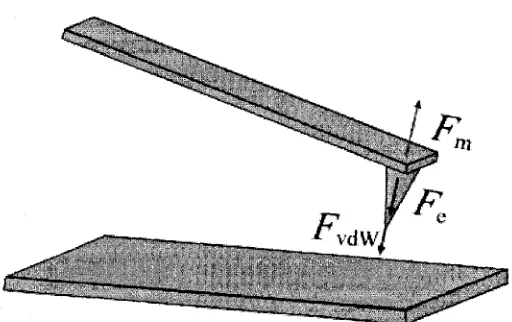
In electrostatic operation the deflection profile of an AFM probe depends on various
forces such as electrostatic forces Fe due to the bias voltage, van der Waals short range
interaction forces Fvdw, and cantilever mechanical restoring force Fm. The AFM probe-substrate system is schematically shown in figure 8 together with the forces acting on the
probe.
Figure 8. A schematic diagram of AFM probe-substrate system
showing different forces acting on AFM probe.
The total energy of the AFM probe-substrate system is the algebraic summation of the
energies associated with different force components as shown in figure 8 and can be
expressed as:
ET=Em-Ee~ Evdw (7)
where Ee represents energy associated with electrostatic force, Evdw represents energy
associated with van der Waals forces and Em represents energy associated with
2.2.1 Mechanical Bending Energy
The mechanical strain energy of the AFM probe-substrate system can be expressed as:
rEI a w
Em = J -T —2" <& (8)
o z v "* y
where E, I, L, and w represent effective Young's modulus, cross sectional area
moment of inertia, beam length, and beam deflection as a function of axial position JC ,
respectively. Effective Young's modulus E is equal to the plate modulus E/(\ - V2) for
wide beams (w>50, where E, and v represent the Young's modulus and Poison's ratio
of the beam material, respectively and w, and / represent the beam width and thickness,
respectively. For narrow beams E simply becomes the Young's modulus E. Equation
(8) is based on the assumption of Euler-Bernoulli cantilever beam which requires that
L»w mdL»t. AFM cantilevers beams are usually wide and fall into
Euler-Bernoulli limit.
2.2.2 Electrostatic Energy
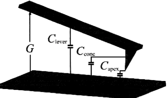
The electrostatic energy of the AFM probe-substrate system Ee can be expressed as:
Ee=\cTV2 (9)
where CT is the total capacitance associated with the AFM probe and the substrate
system and V represents the applied bias voltage. The total capacitance CT can be
C =C A-C A-C (10)
where Clever, Ccone, and Capex represent the capacitances between the cantilever beam and substrate, the capacitances between the tip cone and substrate, and the capacitances
between the spherical tip apex and substrate respectively as shown in figure 9.
Figure 9. A schematic diagram of the AFM probe-substrate system
showing various capacitance components.
2.2.3 Van der Waals Energy
Following [17], the van der Waals energy of the AFM probe-substrate system can be
expressed as:
Jvdw
A | (l + tanz6>) R
30 z + /!(!-sin0) z< (11)
where A is the Hamakar constant which depends on the material properties of the tip
Van der Waals force becomes negligible when the distance between AFM tip and
substrate is more than a few nanometers [18]. As the collapse of the AFM probe due to
the electrostatic force takes place at a much higher distance between the AFM tip and the
substrate, in typical analysis the energy associated with the van der Waals force is
neglected. Accordingly, this analysis is focused on the investigation of the probe collapse
due to the electrostatic and the mechanical restoring energies only.
Chapter summary
In this chapter the fundamental geometrical configuration of an AFM probe-substrate
system has been presented. The considerations and assumptions that have been taken into
account for the development of the closed-form analytical model to determine the pull-in
voltage of an AFM probe are also presented. As the first step of the model development,
different capacitances, forces, and energies associated with these different forces have
been identified. Then the mathematical expressions for different energies, such as van der
Waals energy, mechanical bending energy, and electrostatic energy are presented. These
mathematical expressions are used in the next chapter to develop a more accurate model
CHAPTER 3
ELECTROSTATIC ENERGY MODELING
This chapter develops a more accurate model of the electrostatic energy stored in the
AFM probe-substrate system after applying a bias voltage. At first a capacitance model
has been developed to determine the capacitance between the AFM probe cantilever and
substrate. The capacitance model takes account of the fringing field capacitances
associated with the cantilever to realize a more accurate energy expression for the system
as the fringing field capacitances were neglected so far in the published literature while
deriving the energy stored in an AFM probe-substrate system. This chapter also presents
capacitance models associated with AFM probe tip cone and tip apex. And finally all the
capacitance models have been used to derive a more accurate electrostatic energy model
for an AFM probe-substrate system.
3.1 Capacitance Associated with AFM Probe cantilever
In a typical geometry, the cantilever beam of an AFM probe-substrate system is inclined
at an angle Piever with respect to substrate plane as shown in figure 10. Since the gap
between the cantilever and the substrate is variable along the beam axis, following
[18-19] the capacitance between the AFM probe cantilever and the substrate can be expressed
as:
L r w
Figure 10. Schematic diagram of AFM probe cantilever arrangement.
where g(x) is the variable gap between cantilever and substrate and can be expressed as:
g(x) = z + Hcosfilever + Lsin/3lever - xsmfilever (13)
where z is the distance between the tip apex and the substrate.
Another model [12, 20] expresses the capacitance between the AFM probe cantilever and
the substrate as:
r gpwtan (Piever) ,J, , 2£tan(lf e v e r/2)
^lever (14)
Both of these models have neglected the fringing field capacitance between the cantilever
and substrate. However, as the fringing field capacitance becomes a significant
contributor to the stored electrostatic energy if the beam is narrow [22], a capacitance
However, there is no straight-forward accurate analytical solution is available to compute
the fringing field capacitance associated with a beam-substrate system except
computationally highly expensive numerical methods. However, some approximate
closed-form models are available in literature that can calculate the total capacitance
including the fringing field capacitance of a VLSI on-chip interconnect separated form
the substrate by a thin dielectric material. Since a square cross-section beam separated
from a fixed ground plane by a thin airgap and a VLSI on-chip interconnect separated
from the substrate by a thin dielectric has similar geometric configuration, models for
computing the capacitance associated with a VLSI on-chip interconnect can readily be
adopted to determine the capacitance associated with a beam-airgap-substrate system. A
conformal transformation method has been used in [23] to derive relatively simpler
equations to compute the capacitance of a long straight rectangular cross-section VLSI
on-chip interconnects. The method—known as the Chang's formula—is considered the
most accurate closed-form method to date [24] and the accuracy is within 1% of the
values as numerically computed in [25] as long as w>d0 holds where d0 is the gap
between the interconnect and substrate. However, the method is computationally more
expensive when compared to the methods proposed in [26-28]. Excellent comparison of
the above methods regarding accuracy and computation time is available in [24] where it
was determined that Meijs and Fokkema's method proposed in [26] is superior to the
methods proposed in [26-27] in terms of accuracy, validity range, and speed. It has been
determined that the maximum deviation of Meijs and Fokkema's method from the one
developed by Chang is 2% when w/d0 >1, 0A<h/d0 < 4 and 6% as long as
w/d0 > 0.3, h/d0 <10 holds [26]. On the basis of these considerations, the formula proposed by Meijs and Fokkema has been adopted for this analysis.
Following [26], the capacitance between a VLSI on-chip interconnects separated from the
substrate by a dielectric medium can be expressed as:
C- — £()£/•
r,..\ f„,\0-25 f*\0-5
W 1 + 0.77 + 1.06
G)
w
VGJ
+ 1.06 t
where the first term on the right hand side of (15) is the parallel plate capacitance,
second term is an length dependent adjustment parameter, third term is the fringing field
capacitance due to interconnect width, and the fourth term is the fringing field
capacitance due to interconnect thickness. In (15) s0 and sr represents the permittivity
of free space and the relative permittivity of the dielectric spacer, respectively.
As for the AFM probe geometry, the gap between the inclined beam and the substrate
isn't uniform, (15) cannot be used readily to determine the capacitance between an AFM
probe cantilever and the substrate. However, the nonuniform gap along the axial direction
of the beam can be incorporated in (8) to calculate Ciever as:
Clever ~ J ^ 0 ^ 0
W \
G-w)
r
+ 0.77 + 1.06 w
\0.25
G-w)
f
+ 1.06 t
G-w
0.5
+ £r01.06>d t
v0.5
G-w,
(16)
where G represents the initial gap between the cantilever and the substrate and can be
expressed as:
G = w0 + Hcos/3[ever + Lsinj3[ever - xsm.ple (17)
where w0 is the initial distance between the tip apex and the substrate. The last term in
3.2 Capacitance Associated with AFM Tip Cone
Following [30], the capacitance associated with the tip cone and the substrate can be
expressed as:
CCone - 2 ^ 0 " '
where
(w0 +b — w)< In
WQ+b-w^
H -1 > + (WQ -w)- clog(w0 + b-w) (18)
'b = R(\-sw&),
„ cos20
c = R
sin^
n = nq ,
q2 = [ln{tan(0.5^)}]"2
(19)
The parameters b, c, n, and q are functions of radius R of the spherical tip apex and
the half-opening angle 9 of tip cone. These two parameters are constants for a specific
AFM probe geometry.
3.3 Capacitance Associated with AFM Tip Apex
Following [30], the capacitance associated with the spherical tip apex and the substrate
can be expressed as:
Capex ~£0m^n
WQ + b — W
WQ -W ~\
(20)
where m is a function which depends on the radius R of the spherical tip apex and can
be expressed as:
3.4 Electrostatic Energy of AFM Probe-Substrate System
The electrostatic energy stored in the AFM probe-substrate system can be calculated by
using the capacitance models associated with the AFM probe cantilever, tip cone and
spherical tip apex with respect to substrate. Total capacitance CT of the system can be
determined by substituting (16), (18), and (20) in (10) and the stored electrostatic energy
then can be determined following (9) as:
Ee=\e0V2 w
\
G-w) + 0.77 + 1.06
/ x0.25
' W x
G-w + 1.06
f t ^ 5
G-w) dx
1.06w
/ \0.5 t
\G{L)-wj
+ 2n\ (WQ +b-w)\ In WQ +b-W
H
i,\ \
+ (WQ -w)-cln(w0 +b-w)\
+ m\n WQ +D-W
V WQ-W y
(22)
Chapter summary
An improved model to predict the electrostatic energy in an AFM probe-substrate system
has been developed by developing a new capacitance model for the capacitance between
the AFM probe cantilever and substrate that includes the energy associated with the
fringing field capacitances. This more accurate representation of the stored electrostatic
energy is then used to develop a highly accurate closed-form model for the pull-in
voltage of the AFM probe as described in the next chapter. Capacitance models
associated with AFM probe tip cone and tip apex, which are necessary for calculating the
CHAPTER 4
PULL-IN VOLTAGE MODELING
This chapter develops a readily computable closed-form analytical model to determine
the pull-in voltage of an Atomic Force Microscope probe. At first total energy of the
AFM probe-substrate system has been determined. Then the formulations for the
deflection shape of an AFM probe cantilever beam under electrostatic pressure are
provided. Finally the mathematical operations needed to develop the closed-form
analytical model to predict the pull-in voltage for the AFM probe has been described.
4.1 Total Energy of AFM Probe-Substrate System
After biasing, the electrostatic attraction force pulls the AFM probe towards the substrate
while the elastic restoring force opposes any deformation of the beam. The net force
working on the beam is the algebraic summation of these two forces. Thus at equilibrium,
the total energy of the AFM probe-substrate system is the net energy associated with the
net force and can be derived from the expressions for the electrostatic and the mechanical
restoring energies. Following this approach, using (7), (8), and (22) and neglecting the
E
T=\
L ~ f ' \ 2
w
2{dx
2dx
2 U
w
Jo \{G-w
+ 0.77 + 1.06
/ \0.25 ' W N
G-wJ
+ 1.06f t A0-5
G-w dx
+ 1.06w t *
G(L) - w
+ 2n< (w0 +b-w) In
V v H
- 1 + (WQ -W)-C ln(w0 + 6 - w)
+ wln WQ + 0 - W
V WQ- W y
(23)
The pull-in voltage can be determined from the second derivative of the total energy
stored in the system. However, due to the presence of the nonlinear terms in (23), it is
very difficult to derive an exact analytical solution for the pull-in voltage from (23).
Investigation shows that the nonlinear terms in (23) can be linearized using the
well-known Taylor series expansion method to obtain a sufficiently accurate analytical model
for the desired pull-in voltage. Following this approach, expanding the nonlinear terms in
(23) by Taylor series about the zero deflection position of the tip, ( w = 0), one obtains:
E
T=]
o
EI_
2
d w
\ CtX i
dx
2 °
eL f 1 w W W W W W . - 3 ~4 - 5 - 6 ^ —r H + + - A G3 G4 G5 G6 G1 j
dx + I 0.77'dx
+ |l.06w0-25 1 0.25w 5wz 15w+ — r ^ i r + ^rr + - J + - I95wq
663wJ 464 lw°
8192G525 65536G6'25
dx
+
Jl.06r°~
1 0.5w 3wl• + — n r + - 5w* 35w* • + • + •G0 . 5 G1 . 5 8 G2 . 5 1 6 G3 . 5 1 28 G4 5
+ 63 w5 23 lw
6 ^
• +
256G55 1024G6'5
+A dx
•l.06wt 0.5 + • 0.5w 3wz • + — • + - 5w* • + - 35w
G/ ^ i tr<T\ oLr(0.5 s-< 1.5 Q/~< 2.5 < s-f--< 3.5 n o / - i 4.5 T\ 1 0 ( j / n l Z o O v
'W \L) \L) \L) T(L)
+ • 63w5 • + - 23 lw6
256G( L ) 5 5 1024G(L)6-5
+ A
+ 2n\ (WQ + b)\ In WQ +b
H flJ
^
+ w0 - cln(w0 +b) + •In
w0 +6
V V H j - 1 + -w0 + ^ w
+ 1 c • +
-2(w0+6) 2(w0+bY
w2 + 1 c • +
-6(w0+by 3(w0+by w
+ 1 c +
12(w0+^)3 4(w0+6)4
~4
W + 1 c
+
20(w0+b)4 ' 5(w0+b)5 w
+ 1 c • +
-30(w0+&) 6(w0+6)
w6+ A
+ m<ln w0 + b + w + ^ - w + — - — — w & „ 2wn b + b „-> 3wft b + 3wr,b +b A^
WQ ( W Q + b) 2WQ (WQ + 6 ) 3w0 (.wo +b)
4w03b + 6w02fr2 + 4w0b3 + b4 „4 5w04b + \0w03b2 + \0w02b3 + 5w0b4 +b5 ,s
6w05b + 15w04b2 + 2 0 w0V + 1 5 w0V + 6wQb5 + b6 „6 A
+ —y y _ J L _ ^ y w° + \
6WQ (WQ + b)
(24)
As the contribution to the total energy from the fifth and higher order terms obtained after
Taylor series expansion is several orders of lower magnitude compared to the initial
terms, truncating the fifth and higher order terms in (24) won't introduce significant error
while result in a more compact and easier energy expression. After truncating the fifth
and higher order terms in (24), one obtains:
£ r = J — rEI
2
fd2w^
o ydx j
dx
l-sQV2
2 °
1 W W W W
w — + —- + —- + —- +—7
[G G2 G3 G4 G5 J
dx+ \0.77dx
+
jl.06w°
25 1 0.25 w 5w• + TXT- + T ^ +z 15w TTT-J 195w + 4 >G0.25 G1.25 22G225 128G325 2048G425
ax
+
J1.0&
0-
5- 2 c - . 3
1 0.5w 3wz 5wJ 35w . . . 4 N\
+ ——+ " • + • • +
-VG0 5 GL5 8G2'5 16G35 128G4 5 y
dbc
+ 1.06wf 0.5 1 0.5w 3wz-+ r r + ^-r + r r + 5w3 35wH G 0.5 /nr 1.5 a/*1 ^*5 -i >r/^ <3«5 i '*>o/~' 4.5
(L) °"(L) 8 C r( I ) 1 6 ( j r(Z,) l ^ » G( i )
+ 2« (w0+6) In
WQ +b
H - 1 + w0 -cln(w0 + b) +
(
- l n f ^ l - l
+- °
H WQ +b W
+ 1 c • +
-2(w0+b) 2(w0+b):
~2
W + 1 c • +
-6(w0+by 3(w0+bY w
+ f 1 c ' r + : I2(w0+by 4(w0+b)
w4 >
+ m<\n w0 + b ™0 ,
+ • Iw^b + b
2 ,2 3 w0 2i + 3 w0i2+ &3 . 3
W+ ;r ^W + - W w0(w0+b) 2w02(w0+by 3w0 (W0 + b)
A<V(?b + 6wf?b2 + 4wnb3 + b4 A 4
+ — - ^ j w
4w0 (w0 + 6)
(25)
4.2 Pull-in Voltage Closed-Form Model
The deflection profile function of a cantilever beam can be expressed as [31-32]:
w(x) = YjPn<pn(x) (26)
where <pn (x) is the nth assumed deflection shape function that satisfies the boundary
conditions and the coefficients Pn are the weighting of the associated mode that are to be
determined. For free vibration of structures, the natural mode approach provides the exact
solution to the vibrational amplitude and deformation shape as it satisfies the boundary
conditions and the homogenous part of the governing equation of a dynamic system [33].
The natural mode approach also provides the foundation for forced response calculation
in structural dynamics [33]. Moreover, as the electrostatic force due to the biasing voltage
attracts the beam towards the ground plane; this kind of deformation is similar to the first
natural mode of the beam. These considerations prompt to choose the first natural mode
of cantilever beam as the deflection shape function.
Following [31-32], the first natural mode of a cantilever beam can be expressed as:
9\ (x) = [cosA(&jx) - cos(A:1x)]
-sinh^Z,) - s i n ^ Z )
where the coefficient kx represents the flexural wave number of the first natural mode
and satisfies the following relation:
cosh(A:1Z)cos(A:1Z) - - 1 (29)
In (29) kxL& 1.875 is the wave number of first natural mode times the length of the
cantilever. Substituting (27) in (26) the deflection function of the AFM probe cantilever
can be given by:
M.x) = Pm(
x)
(30)where Px is the weighting of the first natural mode that is to be determined. Renaming Px
and (pi(x) as P and (p(x) , respectively, (30) can be re-written as
w(x) = P(p(x) (31)
The total energy ET of the AFM probe-substrate system thus can be expressed in terms
of P and cp(x) by substituting (31) in (25) as:
E
T=]^-(P<p")
2dx
o
z2 U w\
1 Pep {PcpY {Pep)' (Pep)
1 — -j 1 1
G G2 G3 G4 4 \
dx
+
]l.06w
025 1 0.25i> 5(P(pY \5(P(py \95(Pcp)4 \
VG0-25 GL25 32G2 2 5 128G325 2048G4'25 j
+
Jl.O&°"
1 | 0.5P<p | 3(P(P)1 | 5(P<py | 35(/»4A
G0.5 G1.5 8C?2.5 1 6 G3 . 5 1 28 G4 5 \dx
+ 1.06wfa5
^ 1 | 0.5P(p{L) | 3 ( i y( I ))2 | 5{P<p{L)f | 3 5 ( / >( z ))4^
G O.5 /—i 1.5 o/^1 2.5 i srs^i 3.5 1^0/^4.5
cr\ Czm o u v n loUv/^ 1 Z O ( J
7(i) ^ ( i ) T(L) T(L)
+ 2n\(w0 +b)ln — - 6 - c l n ( w0+ & ) +
l V H )
- I n w0 +6
V V H j
•1+-w0 +b P<P{L)
+
1 C
-+-2(w0+b) 2(w0+bY (P<P(L))
2 +
1 c • +
-6(w0+b) 3(w0+by
(P<P(L)Y
( 1 c ^ r +
12(w0+Z>r 4(w0+6)
(P<P{L)Y
+ m\ log ' WQ +b^
V ^ 0 y
b „ 2 wn ^ + & . „ . 2
w0(wQ+b) 2w02(w0+b)2
3w02Z>+3w062 +b3 , 4w03Z>+6w0 V +4wn63 +Z>4 4 3w0 (wo+&) 4w0 (WQ +b) (P<P(L))
(32)
Rearranging (32),
where
1.06W0"25 l.06t05]
^
0= J
- +
0.77
+ — ^ - +
,0.5 Jx
0.5
l.06wt _ . . . r x 1
+ — + 2 ^ ( w0+ 6 ) l n
G U) 0.5
^w0 +6^
V # J
• b - c l n ( w0 + b) > + ml In
' w0 + b ^
V ™o j
(34)
4= J
o
' w 0.265w025 0.53t05 ] J "
+
0.53w?0 5
G, XL) 1.5
+ 2«^ - In rWQ +b^
v # J
• 1 + \ + m\ - —
WQ+bj [WQ(wQ+b) <P(L)
(35)
A2=\
o w
G3 32G
5.3w025 3.18? 0.5 A +
2.25 8 G;2.5 #?2d!x;
+
3A8wt0-5
+ 2n\ • +
-8% ) [2(w0+6) 2(w0+fc)'
• + m i 2w
026 + 62
2w0 (WQ + b)
92{L) (36)
A
3=]
G4 1 2 8 G3 2 5 1 6 G3 5 (p dx
+ 5.3wt
0.5 2 , t3
r+2n< +
1 6 G( L ) 3 5 ""[6(wQ+bf ' 3 ( w0+ 6 )3
• + /M-3w0 b + 3wQb +b
3WQ (WQ + b)
<P\L) (37)
A
4=]
( w 206.7w—F + 7^T + JT #> dx 0-25 3 7 . kan 4 /[G5 2048G4"25 1 2 8 G4 5J +
37. \wt 0.5
128G, XL) 4.5
+ 2n\ • + •
12(w0+6)3 4(w0+6)4 >+m- 4w
02b + 6w02b2 + 4w0b3 + bA
4w0 4(w0 +b)A
The system is in a static equilibrium when the first order derivative of the total potential
energy ET with respect to the coefficient P is zero [34]. Taking the derivative of (33)
one obtains after rearrangement:
pJEI(<p")2dx = -£0V2(Al+2A2P + 3A3P2 + 4A4P3) (39)
o 2
Whether the system is in a stable or unstable equilibrium state is determined by the
second-order derivative of the total potential ET with respect to P. At the transition
from stable to an unstable equilibrium, the second-order derivative of the total potential
ET with respect to P equals to zero, i.e. d ET /dP = 0. Rearranging the derivative of (39) one obtains:
J EI(<p"f dx = -e0V2(2A2+6A3P + \2A4P2) (40)
o 2
Dividing (40) by (39) yields:
8A4P3 +3A3P2 -AX = Q (41)
Equation (41) can be solved by Cardan solution [35]. Out of the three roots, two are
imaginary while the real root corresponds to the value of P at pull-in and can be
determined as:
PPI=S + T-^- (42)
where,
S = V M + ylN3 +M2
-Si
T = ^M-^N3 +M
M =
N =
-Al/A4 (A3/A4)2 (43)
16 512
(A3/A4y 64
Substituting (42) in (40) yields the desired closed-form solution for the pull-in voltage
VPI as
PI
R
2\EI((p")2dx
2A2+6A3PPI +12 AAPPI
(44)
Chapter summary
A readily computable closed-form analytical model to determine the pull-in voltage of an
AFM probe has been developed. Taylor series expansion method has been employed to
expand the electrostatic energy and higher order terms in the expansion series have been
truncated to realize a more compact and easier expression of the electrostatic energy.
First natural mode of the beam has been assumed as the deflection shape function of the
beam. An expression for the weighting parameter associated with the first natural mode
of vibration at pull-in has been derived. This expression is then substituted in the second
derivative of the total energy expression. At pull-in, the second derivative of the stored
energy goes to zero. This condition is then utilized to solve the second derivative of the
CHAPTER 5
FEA MODELING
In this Chapter construction of 3-D solid models and meshing strategy of Atomic Force
Microscope probe-substrate system using IntelliSuite™ is presented. The chapter details
the difficulties associated with the construction, meshing strategy, and 3-D
electromechanical finite element analysis (FEA) of the AFM probe-substrate system to
determine the pull-in voltage. The difficulties arise due to the unique geometry of the
system and the mesh size conformity required by the software to accurately calculate the
electrostatic force that causes the pull-in.
5.1 Construction of Atomic Force Microscope Probes
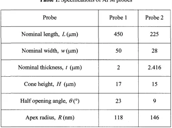
Geometric specifications of two commercially available AFM probes that were modeled
Table 1. Specifications of AFM probes
Probe
Nominal length, L (um)
Nominal width, w (um)
Nominal thickness, t (urn)
Cone height, H (um)
Half opening angle, 9(°)
Apex radius, R (nm)
Probe 1 450 50 2 17 23 118 Probe 2 225 28 2.416 15 9 146
The Interactive 3D Builder is an IntelliSuite module for building and meshing the
three-dimensional geometry of MEMS structures. 3D Builder module of IntelliSuite has been
used to model both the Probe 1 and Probe 2. These probes present a rectangular shaped
cantilever with integrated pyramidal shaped tip cone. The cantilevers are drawn with an
inclination of 21° with respect to substrate.
5.1.1 Geometry of First Probe
The first probe, probe 1 presents AFM probe of cantilever length of 450 micrometer
(um), width of 50 micrometer (urn) and thickness of 2 micrometer (um). The pyramidal
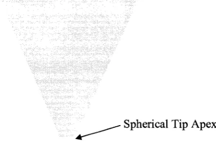
cone has height of 17 micrometer ((am) and of the half opening angle of 23°. The radius
of the spherical apex at the end of the tips is 118 nanometers (nm). Figure 11 shows
different views for the 3-D model for probe 1 that has been constructed in 3D Builder of
AFM Probe
Substrate
(a)
AFM Probe
Substrate
AFM Probe
Substrate
(c)
Cantilever
\
Pyramidal Tip Cone
Spherical Tip Apex
(e)
Figure 11. Geometry of AFM probe 1. (a) Front view of whole of the AFM
probe-substrate system, (b) Side view of the AFM probe, (c) Orthogonal view of the AFM
probe, (d) Side view of the pyramidal tip cone and the part of cantilever, (e) Spherical tip
apex at the end of the tip.
5.1.2 Geometry of Second Probe
The second probe, probe 2 presents AFM probe of cantilever length of 225 micrometer
(um), width of 28 micrometer (jam) and thickness of 2.416 micrometer (um). The
pyramidal cone has height of 15 micrometer (um) and of the half opening angle of 9°.
The radius of the spherical apex at the end of the tips is 146 nanometers (nm). Figure 12
shows different views for the 3-D model for probe 2 that has been built in 3D Builder of
AFM Probe
(a)
AFM Probe
(b)
Substrate
AFM Probe
. Substrate
(c)
Cantilever
Pyramidal Tip Cone
Spherical Tip Apex
(e)
Figure 12. Geometry of AFM probe 2. (a) Front view of whole of the AFM
probe-substrate system, (b) Side view of the AFM probe, (c) Orthogonal view of the AFM
probe, (d) Side view of the pyramidal tip cone and the part of cantilever, (e) Spherical tip
apex at the end of the tip.
5.2 Meshing of Atomic Force Microscope Probes
Meshing is a very critical part of finite element analysis to obtain accurate finite element
analysis simulation results. One critical requirement for proper meshing is that both the
conductors associated with the electrostatic analysis must have reasonably identical mesh
conformity. The AFM probe-substrate system is a very complex structure to mesh due to
geometric properties of AFM probe and the inclination of the AFM probe cantilever with
respect to substrate. Different parts of AFM probes have different dimensions ranging
from a few hundred micrometers associated with the cantilever geometry to some
analysis, both the conductors must have reasonably identical meshing to compute the
electrostatic force accurately, the substrate region under the spherical cone tip must have
reasonably identical mesh structure as the spherical cone tip. However, as the spherical
cone tip has a radius of less than 200 nm for the probes under consideration, refining the
substrate mesh to that scale makes the problem size extremely large to be solved using
even high performance machines with 4 GB of memory. On the other hand, the substrate
region under the cantilever has almost similar dimensions.
For these reasons, using the local mesh refinement feature of IntelliSuite, different part of
the structure are meshed in such a way that maintains a reasonably identical mesh
structure between the exposed faces where electric flux lines are supposed to terminate.
To realize these meshes, each probe has been divided into three separate geometries
containing the cantilever, the pyramidal tip cone and the spherical tip apex. Despite this,
due to the nm scale dimensions of the spherical cone apex, it was difficult to achieve
reasonable mesh conformity in the region between the spherical tip apex and the
substrate. To overcome this, a novel feature of IntelliSuite, called Elec_mesh has been
used to activate the Exposed Face Mesh algorithm (EFM). When compared to the
commonly used volume refining mesh method, the EFM algorithm shows substantial
improvement in increasing accuracy of results and reducing computational time and
memory expenses. It is to be noted here that in order to calculate the electrostatic pressure
on these Exposed Faces, the commonly used method is to refine the three-dimensional
domain. Unfortunately, the modeling of typical electrostatically activated MEMS devices
using the volume mesh method results in large problem sizes. Instead of refining the
volume mesh, Elecjnesh can be used to refine only the electrostatic surface mesh on
chosen Exposed Faces. The advantage of this novel method is that the electrostatic
surface mesh is separated from the mechanical volume mesh while assuring full
compatibility between the two. The EFM method results in smaller computational models
while improving the numerical accuracy in MEMS simulation. Actual refinement process
depends on the refinement factor. Selecting a refinement factor of 4 actually refines the
mesh 2xN or 32 times. Also, additional simplification can be made to the electrostatic
allow that face to have no mesh, thus removing it from the electrostatic analysis. As the
bottom surface of the substrate isn't contributing to any electrostatic force for the probe
deflection, removing the electrical mesh from that surface will reduce the problem size.
Similarly, the fixed face of the probe (rigid support end) also isn't contributing to the
electrostatic force for the probe deflection. Thus removing the electrical mesh from that
face also reduces the problem size. To model the electrostatic force more accurately, the
substrate region near the probe tip has been refined sharply using this electrical mesh
feature to achieve reasonable mesh conformity between the spherical cone tip and the
substrate. A refinement factor N=6 for the tip cone and the spherical tip apex and N=4 for
the substrate region near the probe tip have been used for the electrical mesh.
5.2.1 Meshing of the Probes
Both the probes are meshed following the strategy described in the previous section.
Figure 13 shows the meshed geometry of the AFM probe 1 and figure 14 shows the
meshed geometry of the AFM probe 2. Both the figures highlight the local mesh
refinement at different parts of the structures. In the figures, the triangular panels
represent the electrical mesh that is superimposed on the original quadrilateral
(a)
(c)
(d)
Figure 13. Different mesh sizes for different part of AFM probe 1. (a) Front view of the
meshing of the AFM probe and the substrate, (b) Side view of the meshing of the
pyramidal tip cone and the substrate, (c) Front view of the meshing of the tip apex, (d)
(a)
(c)
(d)
Figure 14. Different mesh sizes for different part of AFM probe 2. (a) Front view of the
meshing of the AFM probe and the substrate, (b) Side view of the meshing of the
pyramidal tip cone and the substrate, (c) Front view of the meshing of the tip apex, (d)
Chapter Summary
In this Chapter detailed construction and meshing strategy of 3-D solid models of two
AFM probe having different geometric specifications using the IntelliSuite™ 3-D
builder™ has been presented. Difficulties associated with the meshing of the structures
have been discussed. To achieve reasonably conformal meshing between the cantilever,
cone, spherical cone apex, and the substrate, local mesh refinement has been used.
Further refinement was carried out using the IntelliSuite's novel Elec_mesh feature that
allows refining the electrical mesh only to a very high factor and then superimposing the
refined electrical mesh in the form of triangular panels on the original quadrilateral
mechanical mesh. This reduces problem size considerably, improves accuracy and
minimizes analysis time and memory expenses. The meshed geometry is then used to
![Figure 3. Microfabricated cantilever beam [13]. (a) Before pull-in, (b) After pull-in](https://thumb-us.123doks.com/thumbv2/123dok_us/1466783.1179716/21.614.164.494.572.673/figure-microfabricated-cantilever-beam-pull-b-pull.webp)
![Figure 5. A schematic diagram of the AFM probe model used in [12] showing parameter](https://thumb-us.123doks.com/thumbv2/123dok_us/1466783.1179716/22.615.108.515.279.557/figure-schematic-diagram-afm-probe-model-showing-parameter.webp)