Analysis of Various Low-Voltage High
Impedance Gate Driven CMOS Current
Mirrors
Nitika Mahajan1, Jasbir Kaur2
P.G. Scholar, Department of E&CE, PEC University of Technology, Chandigarh, India1 Assistant Professor, Department of E&CE, PEC University of Technology, Chandigarh, India2
ABSTRACT: Current mirror (CM) circuit has served as the basic building block in analog circuit design since the introduction of integrated circuit. In this paper, various low-voltage, high impedance gate-driven current mirror circuits have been discussed. The circuits are implemented in GDPK 180nm CMOS process and the simulation is done using Cadence Spectre. Various parameters of the circuits such as current linearity, output impedance, dc transmission error, power consumption, leakage power etc. have been analyzed and discussed. Analysis of these circuits shows that different circuits can be used in different applications depending upon their characteristics. The total power consumption is reduced by 110% in the improved gate-driven current mirror (CM) design and hence can be used for power efficient applications where as the cascode configuration is best suited for high current swing applications due to its high current linearity range.
KEYWORDS: Low-Voltage, Super Wilson, High Output Impedance, Current Mirror, Gate-Driven, Cascode.
I. INTRODUCTION
In the early 1980s many experts predicted the demise of analog circuits. Many functions that had been traditionally realized in analog form were now easily implemented in the digital domain, suggesting that with enough capability in IC fabrication, all processing of signals would eventually occur digitally. But still analog designers are of great demand today. This is because there are many areas where it is not feasible or even impossible to replace analog blocks with their digital counterparts regardless of the technology advancements. Digitization often requires analog blocks before digitizing. A major component in these analog circuits is the current mirror CM), especially a high impedance CM in the case of biomedical applications.
With the advancements in the CMOS technologies, it is possible to integrate baseband signal processing units, sensors and radio-frequency (RF) circuits on a single chip. Ultra-low power consumption and low voltage supply of 1V or less are an important aspect to ensure that the batteries can work for a long duration. The new deep sub-micron CMOS technologies are very apt to fulfil this need, since deep sub-micron CMOS transistors can operate in weak inversion region (up to the GHz region) with reasonable gain, and have low threshold voltage which makes it feasible to design analog circuits that can operate at low voltages (around 1V). However, the scaling of the supply voltage along with the low output resistance of transistors in these deep sub-micron CMOS processes make it very difficult to implement CM and current sources or sinks that give very-high output impedance over a large output voltage range [1]. Various current mirror designs are hence analysed for different parameters and their suitable applications are mentioned.
The performance of the gate-driven current mirrors and their basic operation is described in section II. The simulation results are shown in section III and the conclusions are drawn in section IV.
ISSN(Online): 2320-9801
ISSN (Print): 2320-9798
I
nternational
J
ournal of
I
nnovative
R
esearch in
C
omputer
and
C
ommunication
E
ngineering
(An ISO 3297: 2007 Certified Organization)
Vol. 3, Issue 6, June 2015
shown in Fig. 1. The transistors M1 and M4 forms a CM which samples the output current Iout and makes its
comparison with the input current Iin. The gate voltage of the M5 is adjusted by the difference between Iout and Iin which
in turn assures that the output current Iout is equal with input current Iin.
The output impedance is directly proportional to the gain of the loop which is given as the combination of current source load and Common Source amplifiers M1. The output impedance rout of the HSSWCM can be approximated as:
rout = gm1r01r05 (1)
Where gm1 and r01 are respectively the transconductance and the output resistance of transistors M1 and r05 is the
output resistance of transistors M5. The low voltage current mirror [3] circuit shown in Fig. 2 is the modified super– Wilson structure. In this structure, a diode connected transistor is attached at the input current arm in the cascoded configuration, such that the gain is improved to gmrout. In both cases the auxiliary current source is used to make the
drain symmetry for the CM transistor pair.
Fig. 1 HSSWCM Circuit Fig. 2 LVSWCM Circuit
III. CIRCUITOPERATION
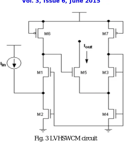
The above circuit acts as a basis for a new circuit low voltage high swing Super Wilson Current Mirror circuit (LVHSSWCM) [4]. In this circuit, no auxiliary current source is required to achieve the drain symmetry for the transistors M2 and M4. Rather, the auxiliary current source is replaced by the diode-connected PMOS to achieve the drain symmetry. The M2 and M4 transistors formed as part of the CM have a purpose of giving high output impedance.M1, which is a diode connected transistor, is modified as a cascoded one. The transistors M2 and M4 samples the output current Iout which is then compared withthe input current Iin which in turn changes the conduction of
the transistor M5 and finally, the output current Iout is made equal to the input current Iin. M6 and M7, which are also
the diode connected transistors, acts as an active load and increase the output impedance as well as the output current. The increased output impedance can be expressed as:
≈( || ) (2)
where gm1, gm2, gm6 and go1, go2, go5 are respectively the transconductance of the transistors M1, M2, and M6.
The performance of the earlier proposed circuits is good in the input current range of 30 to 40μA. However, at
lower input currents, a negative leakage current exists in these circuits due to which these circuits fail to produce the exact mirroring. As a diode connected PMOS is present in LVHSWCM circuit, this performs well in the lower input
range from 5μA to 40μA range as well and provides very less transfer error compared to the earlier mentioned structures..
Fig. 3 LVHSWCM circuit
For the PMOS to act as constant current source, it should be in saturation. i.e. Vgs –Vt≥ Vds,sat (3)
In this circuit Vgs is zero and hence the equation reduces to –Vt≥ Vds,sat (4)
This limits the value of overdrive voltage, Vov depending on the value of Vt to make the transistor operate in the
saturation region.
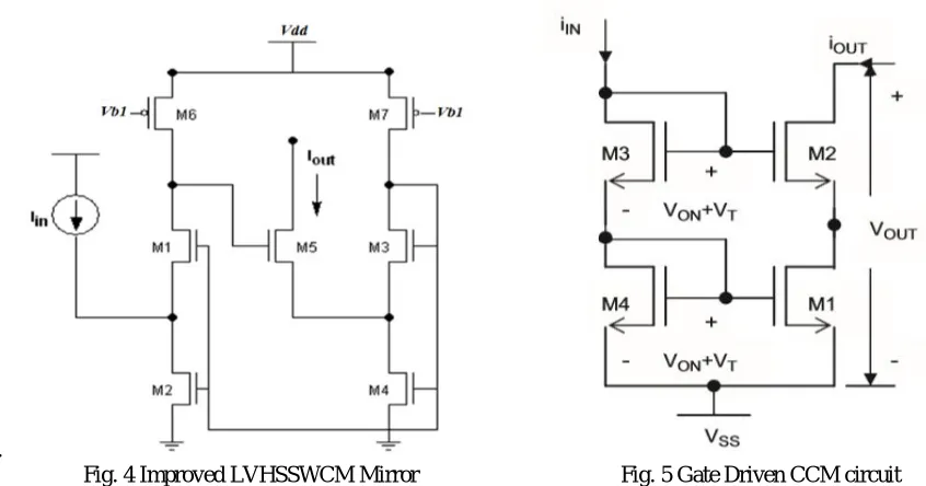
In order to overcome this limitation, LVHSWCM circuit is modified so that the circuit can be designed for various overdrive voltages [5]. The modification is made by removing the short circuit between gate and source of the PMOS transistors and the transistors are biased by applying a biasing voltage at the gate of the PMOS transistors in Fig 4. This helps in designing the circuit for different overdrive voltages. The new current mirror circuit has a biasing voltage Vb1
at the gates of transistors M6 and M7. This voltage is selected such that the transistors obey the condition for saturation, i.e.
Vgs –Vt≥ Vds,sat (5)
Where, Vgs = Vg-Vs=Vb1-Vdd (6)
i.e. the biasing voltage is greater than supply voltage plus minimum overdrive or minimum saturation voltage. Another type of low-voltage, high-swing current mirror is cascode current mirror [6]. The circuit is shown in Fig. 5. Cascode current mirror (CCM) is used to obtain better input/output characteristics. It also helps to achieve high output impedance. In this configuration, the output resistance of the circuit is increased by a factor given by gmr0, (where gm is
transconductance and r0 is output resistance of the MOSFET) [7]. Thus CCM is highly suitable for applications such as high performance second generation current conveyers, variable gain low noise amplifier, voltage to current converter,
telescopic opamps, etc, as compared to simple current mirror. [8]. However, CCM has reduced voltage swing. Let, Vout
be the minimum output voltage needed to maintain the MOSFET’s of the CM in saturation region be. Lower the value of Vout, higher is the voltage swing of the mirror.
The output impedance of this circuit is given by:
ISSN(Online): 2320-9801
ISSN (Print): 2320-9798
I
nternational
J
ournal of
I
nnovative
R
esearch in
C
omputer
and
C
ommunication
E
ngineering
(An ISO 3297: 2007 Certified Organization)
Vol. 3, Issue 6, June 2015
.
Fig. 4 Improved LVHSSWCM Mirror Fig. 5 Gate Driven CCM circuit
IV. SIMULATION RESULTS
The circuits shown in this paper are simulated using Cadence spectre of 180nm CMOS technology. The design specifications are shown in Table I. All the gate driven current mirrors operates at 1.8V.
The output characteristics i.e., output current vs. output voltage is shown in Fig. 6. It can be seen that the circuit starts conducting at a value quite below the threshold value thus reducing the input/output voltage drop.
The Design specifications for LVHSSWCM and improved LVHSSWCM are mentioned in Table I and Table II respectively.
Cascode current mirror has all NMOS of dimension W/L=1µ/180n.
Table I. Design Specifications of LVHSSWCM Table II. Design Specifications of Improved LVHSSWCM VDD= 1.8V, VSS=0V
Transistor Aspect Ratio, W(µm)/L(µm)
PMOS (M6/7) 1/0.18
NMOS (M1-M5) 0.4/0.18
Fig. 6 shows the output characteristics of the circuits. LVHSSWCM and improved LVHSSWCM have almost same output characteristics where the circuit starts conducting when the input voltage becomes greater than the threshold voltage. Whereas CCM has better response as there is no threshold lag for this circuit and the circuits starts conducting as soon as the input is applied. This is attributed due to the cascode topology of the circuit.
VDD=1.8V, VSS=0V
Transistor Aspect Ratio, W(nm)/L(nm)
PMOS (M6/7) & NMOS (M1/3/5)
405/360
(a) LVHSSWCM (b) Improved LVHSSWCM
(c) Cascode Current Mirror
Fig. 6 Output current vs. Output Voltage characteristics
ISSN(Online): 2320-9801
ISSN (Print): 2320-9798
I
nternational
J
ournal of
I
nnovative
R
esearch in
C
omputer
and
C
ommunication
E
ngineering
(An ISO 3297: 2007 Certified Organization)
Vol. 3, Issue 6, June 2015
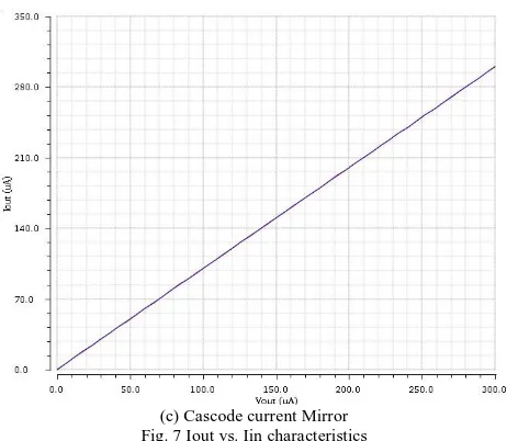
(c) Cascode current Mirror Fig. 7 Iout vs. Iin characteristics
Fig. 7 shows that the linearity of LVHSSWCM is upto 60µA, Improved LVHSSWCM is upto 55µA where as it is upto 100µA for the cascode current mirror.
The output resistance graphs for 5µA input current are shown in Fig. 8. It can be seen that the output resistance shoots abruptly to a very high value at very lower voltages for Fig. 8 a) and b) as the circuits are not conducting at this region but beyond this region the output resistance is constant at a considerably high value. In cascode CM, output resistance increases with increase in voltage and attains maximum value at 1.8V.
Fig. 9 shows the total power consumption of the circuit at 5µA input current. The improved LVHSSWCM has less power consumption (in µW) than LVHSSWCM (in mW) where as for cascode CM, power consumption is increasing with the increase in the output voltage.
(c) Cascode Current Mirror
Fig. 8 Output resistance vs. Output Voltage at 5µA Input Current
(a) LVHSSWCM b) Improved LVHSSWCM
ISSN(Online): 2320-9801
ISSN (Print): 2320-9798
I
nternational
J
ournal of
I
nnovative
R
esearch in
C
omputer
and
C
ommunication
E
ngineering
(An ISO 3297: 2007 Certified Organization)
Vol. 3, Issue 6, June 2015
(a) LVHSSWCM (b) Improved LVHSSWCM
(c) Cascode Current Mirror Fig. 10 Leakage Power Analysis
V. CONCLUSION
The simulation results show that the cascode CM can be used in low supply voltage applications as it reduces the limitation caused by the threshold voltage. Also cascode CM has the highest current linearity (100uA) and can be used in high current swing applications. Improved LVHSSWCM dissipates around 110% less power than LVHSSWCM. Also the leakage power consumption is also reduced by 9 times in Improved LVHSSWCM from LVHSSWCM. Thus the Improved LVHSSWCM is suitable for power efficient or low power applications.
REFERENCES
[1] B. Gosselin, M. Sawan, and C. Chapman, “A Low-Power Integrated Bioamplifier With Active Low-Frequency Suppression,” Biomedical Circuits and Systems, IEEE Transactions on, vol. 1, no. 3, , Sept. 2007, pp. 184–192.
[2] B. Minch, “Low-Voltage Wilson Current Mirrors in CMOS,” in IEEE ISCAS, New Orleans, LA, USA, 2007, pp. 2220–2223.
[3] Louis-Franc¸ois Tanguay, Mohamad Sawan, and Yvon Savaria, “A Very-High Output Impedance Current Mirror for Very-Low Voltage Biomedical Analog Circuits,” Circuits and Systems, 2008. APCCAS 2008. IEEE Asia Pacific Conference, 2008, pp. 642-645.
[4] E. Raghuvaran, “A Very High Impedance Current Mirror For Bio- medical Applications”, IEEE Transactions on Analog Circuits, 2011, pp 828-830.
[5] M.K. Priya, V.K. Vanitha Rugmoni, “A Low Voltage Very High Impedance Current Mirror Circuit and Its Applications”, IEEE ICCCE, 2013, pp. 511-516.
[6] B. Razavi, Design of Analog CMOS Integrated Circuits,McGraw-Hill.