ABSTRACT
HANEY, SARAH KAY. Investigation of Low Temperature, Atomic-Layer-Deposited Oxides on 4H-SiC and their Effect on the SiC/SiO2 Interface. (Under the direction of Veena Misra and Justin Schwartz).
Silicon carbide has long been considered an excellent substrate for high power, high temperature applications. Fabrication of conventional MOSFETs on silicon carbide (SiC) relies on thermal oxidation of the SiC for formation of the silicon dioxide (SiO2) gate oxide. Historically, direct oxidation was viewed favorably due to ease of fabrication. However, the resulting MOS devices have exhibited significant interface trap densities, Dit, which reduce effective inversion layer mobility by capturing free carriers and enhancing scattering. While nitridation has been shown to reduce Dit, the inversion layer electron mobility of these devices is still limited by the presence of carbon near the interface. Studies have suggested a low mobility transition region between the SiC and SiO2, on the SiC side, attributed to increased carbon concentration resulting from the thermal oxidation of the SiC. In this work, we have investigated the low temperature, atomic layer deposition (ALD) of SiO2 onto SiC compared to thermal oxidation of SiC for the fabrication of MOS devices. Avoiding the carbon out diffusion and subsequent carbon build-up resulting from thermal oxidation is expected to result in a superior, higher mobility MOSFET.
A three-step ALD process using 3-aminopropyltriethoxysiliane (3-APTES), ozone and water was evaluated on silicon and SiC substrates. Ellipsometry and XPS were used to characterize blanket films, and showed good results. Capacitors fabricated on SiC showed the need for optimized post deposition anneals. The effect of post oxidation anneals in nitrogen, forming gas and nitric oxide were examined. The standard nitric oxide (NO) anneal that is used to improve Dit after thermal oxidation was also shown to be the best anneal for the low temperature deposited ALD oxides.
temperature or ambient. All samples analyzed exhibited approximately 2-3nm of transition region on either side of the interface with no evidence of carbon or silicon rich regions. XPS was also used to determine a valence band offset of 2.43eV for the ALD oxide on 4H-SiC.
Lateral MOSFETs were fabricated on 4H-SiC substrates with the following oxidation treatments: thermal oxidation at 1175°C, thermal oxidation at 1175°C followed by a nitric oxide (NO) anneal at 1175°C, and ALD of SiC at 150°C followed by an NO post oxidation anneal (POA) at 1175°C. ALD of the SiO2 was performed using 3-aminopropyltriethoxysiliane (3-APTES), ozone and water. Field effect mobility values were comparable for these samples, suggesting common thermal oxidation steps were still limiting the mobility. As such additional lateral MOSFETs were fabricated without the incoming sacrificial oxidation steps. This sacrificial-oxidation free experiment showed a 15% improvement in peak field effect mobility for the nitrided ALD oxide samples as compared to the nitrided thermal oxides. SIMS of the interfaces revealed nitrogen concentrations of ~6E21 at/cc in the nitrided ALD sample compared to ~4-6E20 in the nitrided thermal sample. This extremely high level of nitrogen incorporation, which is unparalleled in NO annealed thermal oxides, is accountable for the increase in field effect mobility. The low deposition temperature of the ALD oxide causes high levels of carbon incorporation and greater number of dangling bonds at the interface. Both the dangling bonds and excess carbon acts as binding sites for the nitrogen, increasing the nitrogen concentration and resulting in higher mobilities.
Results presented support the use of SiO2 deposited using low temperature atomic layer deposition for improved gate oxides on 4H-SiC MOSFETs given the opportunity for increased nitrogen incorporation. The elevated levels of nitrogen measured in the NO annealed ALD SiO2 sample are unique and are directly attributed to the low temperature ALD process. As such, high peak field effect mobilities can repeatably be achieved with optimization
Investigation of Low Temperature, Atomic-Layer-Deposited Oxides on 4H-SiC and their Effect on the SiC/SiO2 Interface
by
Sarah Kay Haney
A dissertation submitted to the Graduate Faculty of North Carolina State University
in partial fulfillment of the requirements for the Degree of
Doctor of Philosophy
Materials Science and Engineering
Raleigh, North Carolina
2012
APPROVED BY :
___________________________________ Dr. Justin Schwartz
___________________________________ Dr. Alan D. Batchelor
__________________________________ Dr. Veena Misra
DE DIC ATION
This thesis is dedicated to my best friend and husband Sean, to our son Finn and to my parents. The continual encouragement and support that I received from all of you
BIOGR APHY
AC KNOW LE DGMENTS
I wish to express sincere appreciation to everyone at the university and those on my committee who have helped me during my graduate studies. First and foremost, to Dr. Anant Agarwal, who encouraged me to pursue this degree and supported my research for the past 7 years. The support of Dr. Veena Misra, who welcomed me into her group and assumed direction of my research when I was advisor-less was also essential. I am also very grateful to Dr. Justin Schwartz for jumping on board and supporting my work as MSE Co-chair when I feared all was lost. I would also like to recognize Dr. Daniel Lichtenwalner, for always asking good questions and pushing me to question my work, and Dr. Dale Batchelor for being an excellent resource for FIB, TEM sample preparation and characterization questions. Edna Deas also deserves special thanks for being the most organized, caring and helpful person at North Carolina State University.
I am also indebted to my coworkers, past and present, who supported me in this endeavor. Notably Dr. Sarit Dhar, from whom I learned so much about the SiO2/SiC interface and Jeff Whitt, for help with processing all of my tiny pieces in the fab. I am also forever grateful to Dr. John Palmour, and everyone else at Cree who understands the importance of pursuing graduate degrees.
I would like to thank Dr. Juan Carlos Idrobo and Dr. Gerd Duscher from Oak Ridge National Labs for their guidance and assistance with the STEM/EELS data that I have amassed throughout this research. I would also like to thank the ORNL Center for Nanophase Materials Sciences for their support of my work through research grants.
TABLE OF C ONTENTS
LIST OF TABLES ... ix
LIST OF FIGURES ... x
CHAPTER 1: INTRODUCTION AND OVERVIEW ... 1
1.1 Research Motivation ... 1
1.2 Dissertation Structure ... 3
1.3 References ... 5
CHAPTER 2: BACKGROUND ... 7
2.1 Silicon Carbide ... 7
2.1.1 Crystal Structure ... 7
2.1.2 Semiconductor Properties of SiC ... 9
2.2 Interface of SiC and SiO2 ... 10
2.2.1 Oxidation of SiC ... 10
2.2.2 Problems at the Interface of SiC and SiO2 ... 11
2.2.3 Interface Passivation ... 14
2.3 SiC MOSFETs ... 16
2.3.1 MOSFET Operation ... 17
2.3.2 MOSFET Characteristics ... 19
2.3.3 Oxide and Interface Charge ... 22
2.3.4 Non-Ideal Charge Effect on I-V Characteristics ... 23
2.3.5 Non-Ideal Charge Effect on C-V Characteristics ... 25
2.4 Summary ... 26
2.5 References ... 27
CHAPTER 3: RESEARCH METHODOLOGY ... 32
3.1 Atomic Layer Deposition ... 32
3.2 Materials Characterization Techniques ... 37
3.2.1 Ellipsometry ... 37
3.2.2 X-Ray Photoelectron Spectroscopy ... 38
3.2.3 Scanning Transmission Electron Microscopy ... 39
3.2.4 Electron Energy-Loss Spectroscopy ... 42
3.2.5 Secondary Ion Mass Spectrometry ... 45
3.3 Electrical Characterization Techniques ... 45
3.3.1 Capacitance – Voltage Measurement ... 45
3.3.2 Current - Voltage Measurements ... 48
3.3.3 Interface Trap Density Measurement ... 49
3.4 Electrical Modeling ... 52
3.5 SiC Sample Fabrication ... 55
3.5.1 Capacitors ... 55
3.5.2 Lateral MOSFET structures ... 55
3.6 STEM Lamella Fabrication ... 57
3.6.1 Focused Ion Beam Milling ... 57
3.6.2 Lamella Preparation ... 57
3.7 References ... 61
CHAPTER 4: ALD OF SIO2 RESULTS AND DISCUSSION ... 63
4.1 Development of ALD Process ... 63
4.2 Capacitor Results on Silicon ... 70
4.2.1 Ellipsometry ... 70
4.2.2 C-V ... 71
4.3 Conclusions ... 72
4.4 References ... 73
CHAPTER 5: CAPACITORS ON SIC RESULTS AND DISCUSSION ... 74
5.1 Optimization of the Process on SiC ... 74
5.1.1 Effect of Pre-deposition Surface Cleans ... 74
5.1.2 Effect of Post-deposition Forming Gas Anneal ... 76
5.1.3 Effect of Post-deposition Nitric Oxide Anneal ... 78
5.1.4 Electrical Modeling ... 81
5.2 Materials Characterization of the ALD SiO2/SiC Interface ... 82
5.2.1 XPS Results ... 82
5.2.2 STEM/EELS Results ... 88
5.3 Conclusions ... 90
5.4 References ... 92
CHAPTER 6: STEM/EELS INVESTIGATIONS OF THE SIC/SIO2 INTERFACE ... 93
6.1 Investigation of Miscut Effects on Nitrided Thermal Oxides ... 95
6.1.1 Materials Characterization of Nitrided Thermal Oxide on 2 Degree Offcut Material ... 95
6.1.2 Materials Characterization of Nitrided Thermal Oxide on 4 Degree Offcut Material ... 96
6.1.3 Materials Characterization of Nitrided Thermal Oxide on 8 Degree Offcut Material ... 98
6.2 Investigation of Miscut Effects on Nitrided ALD Oxides ... 102
6.2.1 Materials Characterization of Nitrided ALD Oxide on 4 Degree Offcut Material ... 103
6.2.2 Materials Characterization of Nitrided ALD Oxide on 8 Degree Offcut Material ... 105
6.4 Conclusions ... 116
6.5 References ... 117
CHAPTER 7: MOSFETS ON SIC RESULTS AND DISCUSSION ... 118
7.1 Sacrificial Oxidation-Free MOSFET Comparison ... 118
7.1.1 Electrical Characterization ... 119
7.1.2 Electrical Modeling ... 120
7.2 Experimental Verification ... 121
7.2.1 Electrical Characterization ... 121
7.2.2 Electrical Modeling ... 122
7.3 Role of the Nitric Oxide Anneal ... 123
7.4 Conclusions ... 129
7.5 References ... 130
CHAPTER 8: CONCLUSION ... 131
8.1 Description of Findings... 131
8.2 Future Work ... 133
8.3 References ... 135
APPENDICES... 136
Appendix A: EELS Quantification Methods ... 137
Appendix B: Energy band Alignment of ALD SiO2 on SiC... 143
LIST OF TABLE S
Number Page
Table 1.1 Physical property comparison of Si and 4H-SiC ... 1 Table 1.2 Comparisons of SiC MOSFET experimental mobility and Dit
to SiC theoretical and silicon results ... 2 Table 2.1 Material properties of some common SiC polytypes ... 9 Table 2.2 Material properties comparisons of common semiconductors
for power electronic devices ... 10 Table 3.1 Processing parameters for high temperature oxidation recipes56 Table 4.1 Process parameters for SiO2 ALD recipe ... 64 Table 4.2 Ellipsometry data for different surface cleans for ALD SiO2
on silicon ... 70 Table 5.1 Ellipsometry data for different surface cleans for ALD SiO2
on SiC ... 75 Table 5.2 Extracted parameters from capacitance-voltage modeling ... 82 Table 6.1 Comparison of SiC side transition region thickness, SiO2 side
thickness and lateral MOSFET field effect mobility for the three nitrided thermal oxide samples studied ... 102 Table 6.2 Comparison of SiC side transition region thickness, SiO2 side
thickness and lateral MOSFET field effect mobility for the nitrided ALD oxide samples studied ... 108 Table 6.3 Comparison of SiC side transition region thickness, SiO2 side
thickness and lateral MOSFET field effect mobility for the four process splits investigated with the sacrificial oxidation-free
process ... 115 Table 7.1 Comparison of Hauser Mob2d model results for both
LIST OF FIGUR E S
Number Page
Figure 2.1 Illustration of a SiC tetrahedron ... 8
Figure 2.2 Site locations for close packed hexagonal planes ... 8
Figure 2.3 Stacking sequence of 4H, 6H, 15R and 3C silicon carbide in the [1120] plane ... 8
Figure 2.4 Depiction of the charge balance in a SiC MOS system with interface traps illustrated ... 12
Figure 2.5 Depiction of the assumed distribution of interface states at the SiC/SiO2 interface for 4H-SiC, 6H-SiC and 15R-SiC ... 13
Figure 2.6 Depiction of the charge balance in a SiC MOS system with both interface and bulk traps ... 14
Figure 2.7 4H-SiC interface trap densities near the conduction band for varying post oxidation anneal ambients ... 15
Figure 2.8 Schematic of a SiC metal-oxide-semiconductor capacitor ... 15
Figure 2.9 Band offsets for 4H-SiC MOSFETs... 16
Figure 2.10 Schematic of a 4 terminal p-type, n-channel MOSFET ... 17
Figure 2.11 Band diagrams showing the 4 modes of operation for an n-channel MOSFET (a) Equilibrium or Flat band (b) Accumulation (c) Depletion and (d) Inversion ... 18
Figure 2.12 Schematic of a 4 terminal p-type MOSFET showing (a) the depletion region and (b) the inversion layer and depletion regions .. 19
Figure 2.13 Typical MOSFET family of curves showing Id-Vds behavior for varying gate voltages ... 20
Figure 2.14 Typical p-type MOS capacitor high frequency and low frequency C-V curves showing the three regions of operation ... 20
Figure 2.16 Illustration of injection and tunneling mechanisms that can cause leakage in MOSFETs ... 25 Figure 3.1 Schematic of a four step ALD sequence resulting in one
complete reaction cycle ... 33 Figure 3.2 The ALD process window as related to growth rate versus
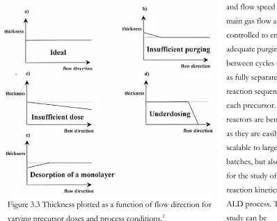
temperature ... 34 Figure 3.3 Thickness plotted as a function of flow direction for varying
precursor doses and process conditions ... 35 Figure 3.4 STEM images. Left: Bright field (BF) image. Right: High
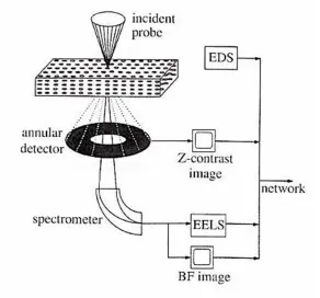
angle annular dark field (HAADF) image. The left side of both images is SiO2 with crystalline SiC on the right side ... 41 Figure 3.5 Schematic of a dedicated STEM showing various detectors .. 41 Figure 3.6 Schematic of an EELS spectrometer and HAADF detector
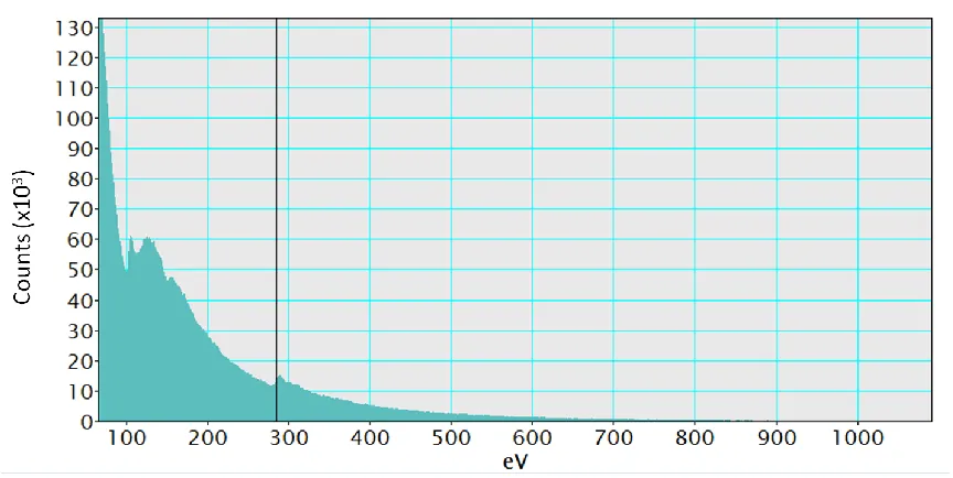
in a STEM ... 43 Figure 3.7 Example spectra of a SiC sample. Peaks include silicon (100
eV), carbon (284.5 eV) and oxygen (532 eV) ... 44 Figure 3.8 Examples of the effect of charges on C-V curves a) C-V
curve with no charge(a), injected charge (b) and mobile charge (c), b) shift in C-V curves caused by injected charges, c) shift in C-V curve due to mobile charges ... 47 Figure 3.9 Sample capacitance-voltage curves from a p-type capacitor.
Both the low frequency and high frequency curves are shown to highlight the different behavior in the strong inversion region ... 50 Figure 3.10 High frequency capacitance measurements taken as part of
Across all measured gate voltages Right: Low voltage region used to obtain the most accurate fit... 54 Figure 3.14 Cross-section of typical lateral MOSFET used for this
research ... 55 Figure 3.15 Left: sample die showing the device patterns. Right: 5x
microscopic view showing circular FETs as well as the gated lateral MOSFET used for this research ... 56 Figure 3.16 View of the TEM lamella preparation before lifting out of
the lateral MOSFET sample ... 58 Figure 3.17 The states of TEM lamella preparation using the FIB a)
pre-polish lamella attached to grid, b-c) polished lamella, and d) top down view of lamella ... 59 Figure 4.1 Proposed 3 step sequence for atomic layer deposition of
SiO2 using water, ozone and 3-APTES ... 63 Figure 4.2 Plot illustrating the 30 pulse ozone line purge sequence ... 64 Figure 4.3 Plot illustrating the beginning of a standard SiO2 deposition
run. The initial 30 pulses of ozone are shown, followed by the 3-APTES, water and ozone pulse sequences... 65 Figure 4.4 Measured “as deposited” ALD SiO2 thickness variation
across half of a 3” wafer. ... 66 Figure 4.5 Variation in refractive index for the “as deposited” ALD
SiO2 ... 66 Figure 4.6 Plot of ψ as a function of wavelength for ALD SiO2 deposited on
silicon ... 67 Figure 4.7 Plot of Δ as a function of wavelength for ALD SiO2 deposited on
silicon ... 67 Figure 4.8 Summary spectrum for “as deposited” ALD SiO2 with Si 2p,
Figure 4.9 O 1s (left) and Si 2p (right) spectrum for as deposited ALD SiO2 with peak fitting ... 69 Figure 4.10 Normalized capacitance-voltage measurements comparing
pre-deposition cleans for ALD SiO2 deposited on silicon ... 71 Figure 5.1 Relative activation energies for –OH removal from silicon surfaces,
Si-face SiC surfaces and C-face SiC surfaces. ... 74 Figure 5.2 Plots of ψ and Δ for the BOE and HF cleans. BOE data is shown in
a) and c), while HF data is presented in b) and d). ... 76 Figure 5.3 Capacitance-voltage measurements for ALD SiO2 capacitors on SiC
after varying forming gas anneals ... 77 Figure 5.4 Normalized capacitance-voltage measurements comparing ALD
SiO2 with varied NO anneal temperatures to ALD with 600˚C N2 post deposition anneal... 78 Figure 5.5 Normalized capacitance-voltage measurements comparing various
anneal treatments for ALD and thermal oxides. ... 79 Figure 5.6 Density of interface traps (calculated from hilo CV) as a function of
trap energy distance from the conduction band for NO annealed ALD SiO2 and thermal oxides with and without NO anneal... 80 Figure 5.7 Breakdown of an NO annealed ALD SiO2 compared to nitrided
thermal oxide on 4H-SiC ... 81 Figure 5.8 Survey spectrum of NO annealed ALD SiO2 on SiC. N 1s peak is
indicative of nitrogen bonding ... 84 Figure 5.9 Silicon 2p spectrum and peak fitting for unannealed ALD SiO2 ... 85 Figure 5.10 Oxygen 1s spectrum and peak fitting for unannealed ALD SiO2 .... 86 Figure 5.11 Carbon 1s spectrum and peak fitting for unannealed ALD SiO2 .... 87 Figure 5.12 Bright field (left) and HAADF (right) images of an NO anneal
Figure 5.13 Relative composition across the SiC/SiO2 interface determined through EELS and the corresponding Z-contrast image showing the sample area ... 89 Figure 5.14 Relative composition across the SiC/SiO2 interface determined
through EELS, the corresponding BF image and intensity profile of the image ... 90 Figure 6.1 Offcut angles of 2,4, and 8 degrees illustrated using STEM HAADF
images and Si-C tetrahedrons ... 93 Figure 6.2 Field effect mobility versus field for the varying offcut nitrided
thermal oxidation samples measured with Vd = 50mV ... 94 Figure 6.3 STEM Images of the 2 degree offcut thermal + NO anneal sample
left: HAADF image, right: BF image ... 93 Figure 6.4 EELS quantification plots and bright field image of the 2 degree
offcut thermal oxidation + NO anneal sample ... 95 Figure 6.5 HAADF image for the 4 degree offcut sample ... 97 Figure 6.6 EELS quantification plots and HAADF image for the 4 degree
offcut sample ... 98 Figure 6.7 HAADF image for the 8 degree thermal oxidation sample ... 99 Figure 6.8 EELS plots, HAADF image and image intensity profile for the 8
degree offcut thermal + NO sample ... 100 Figure 6.9 EELS quantification plots showing silicon, carbon and oxygen
composition, the HAADF image and the image intensity profile for the 8 degree thermal + NO sample. ... 101 Figure 6.10 Field effect mobility versus field for the 4 and 8 degree offcut
nitrided thermal oxidation and nitride ALD oxide samples measured with Vd = 50mV ... 103 Figure 6.11 STEM HAADF image for the 4 degree nitrided ALD sample ... 104 Figure 6.12 Relative composition from EELS and HAADF image for the 4
Figure 6.13 HAADF (left) and LAADF (right) images of the 8 degree ALD + NO anneal lateral MOSFET sample ... 106 Figure 6.14 Relative Composition, HAADF image and Intensity profile for the
8 degree ALD + NO anneal sample ... 107 Figure 6.15 Additional Relative Composition, HAADF image and Intensity
profile for another 8 degree ALD + NO sample shows repeatable EELS results ... 108 Figure 6.16 Capacitance-voltage measurements of the four process splits from
the sacrificial oxidation-free experiment ... 110 Figure 6.17 Plot field effect mobility (calculated from transconductance and
measured with a drain voltage of 50 mV) of the four process splits from the sacrificial oxidation-free experiment ... 111 Figure 6.18 Relative composition from STEM/EELS and HAADF STEM
image from the sacrificial oxidation-free, unanneal thermal oxide process sample ... 112 Figure 6.19 Relative composition from STEM/EELS and HAADF STEM
image from the sacrificial oxidation-free, nitrided thermal oxide process sample ... 113 Figure 6.20 Relative composition from STEM/EELS and HAADF STEM
image from the sacrificial oxidation-free, nitrided ALD oxide process sample ... 113 Figure 6.21 Relative composition from STEM/EELS and HAADF STEM
image from the sacrificial oxidation-free, low temperature annealed, ALD oxide process sample ... 114 Figure 7.1 Capacitance-voltage measurements of the four process splits from
the sacrificial oxidation-free experiment ... 118 Figure 7.2 Plots of Id-Vg (top) and field effect mobility (calculated from
oxidation-Figure 7.3 Experimental data for nitrided ALD oxide compared to calculated data and data modeled with varying interface state densities ... 120 Figure 7.4 Field effect mobility as a function of gate voltage for the nitrided
thermal and ALD oxides from both sacrificial oxidation-free experiments . 122 Figure 7.5 SIMS nitrogen concentration profiles for the nitrided thermal and
nitrided ALD samples from sacrificial oxidation-free experiments 1 and 2 . 124 Figure 7.6 SIMS nitrogen concentration profiles for blanket ALD oxides
annealed in NO at 950 °C for 30 and 120 minutes ... 125 Figure 7.7 Curves of the relationship between mobility and onset of conduction
for nitrided thermal oxides on 4H-SiC. Peak mobility data from this work is included ... 128 Figure A.1 Example of signal, background and edge set up for quantification 138 Figure A.2 Digital Micrograph quantification output graphs as a function of
scan distance. Top: Extracted core-loss signal. Middle: Areal Density. Bottom: Relative composition ... 139 Figure A.3 Relative composition plot with high scan resolution provides more
data at the interface... 142 Figure B.1 XPS C 1s spectra for a thin (2.5 nm) ALD SiO2 on SiC sample and
bulk SiC sample showing good peak alignment ... 144 Figure B.2 XPS O 1s spectra for a thick (16.8 nm) ALD SiO2 and thin (2.5 nm)
ALD SiO2 on SiC sample showing good peak alignment ... 145 Figure B.3 XPS valence band spectra for a thick (16.8 nm) ALD SiO2 and a
bulk SiC sample. The VBM was determined to be 3.39 eV for the SiO2 and 0.96 eV for the 4H-SiC ... 146 Figure B.4 a) Deconvolved energy loss spectra for 4H-SiC showing a bandgap
onset at 3.1 eV b) Published band structure for 4H-SiC showing a bandgap of 3.23 eV ... 147 Figure B.5 Deconvolved energy loss spectra for 4H-SiC showing a bandgap
Figure B.6 Energy band diagram for p-type polysilicon on 16.8nm of ALD SiO2 deposited on n-type 4H-SiC ... 149 Figure B.7 Energy band diagram for a capacitor fabricated with p-type
C H A P T E R 1
INTRODUCTION AND OVE RVIEW
1.1 Research Motivation
Silicon carbide (SiC) MOSFETs have been a long-time goal of SiC research. SiC MOSFETs provide many advantages over traditional silicon (Si) MOSFETs for high temperature, high power applications. The wide bandgap and high thermal conductivity of SiC allow for device operation at high junction temperatures making it particularly suitable for high temperature applications. Simultaneously, the high critical breakdown field provides advantages over Si for both device specific on-resistance and OFF state blocking for high power applications. These benefits are clearly shown in Table 1.1, which
summarizes a few comparisons of Si and 4H-SiC.1,2,3,4
Table 1.1 Physical Property Comparisons of Si and 4H-SiC
Si 4H-SiC
Bandgap (eV) 1.1 3.26
Electron Mobility (at 300K) (cm2/V·s) 1350 950
Critical Breakdown Field (MV/cm) 0.3 2.0
Thermal Conductivity (W/K·cm) 1.5 4.5
interface, associated with excess carbon from the oxidation process. The high Dit causes increased Coulombic scattering which reduces mobility. Additionally before an inversion layer can form, the free electrons must fill all of the interface traps. This further decreases the mobile charge available for conduction. Starting in 1997, anneals in nitric oxide (NO) were shown to reduce the Dit by an order of magnitude.5 Continued studies also revealed a significant increase field effect mobilites from <5 cm2/Vs to 30 cm2/Vs.6 Additional methods of getting nitrogen to the interface have been investigated and have shown similar results with lower Dit and higher field effect mobilities (μFE).7,8,9 In addition to the use of nitrogen to passivate the interface, oxidation in the presence of sodium has also been shown to lower Dit and enhance μFE as compared to oxides grown through dry oxidation techniques.10 These comparisons can be seen below in Table 1.2 which illustrates the experimental results from various oxidation techniques compared to theoretical SiC and Si limits.4,7,10,11,12,13,14
Table 1.2 Comparisons of SiC MOSFET experimental mobility and Dit to SiC theoretical and silicon results.
μFE
@ 300K(cm2/Vs)
μHALL
(cm @ 300K 2/Vs)Dit(eV-1cm-2) @ 0.2eV from Ec
Thermal - Dry ≈ 5 ≈ 40 2 x 10¹³
Nitric Oxide Anneal
≈ 35 ≈ 60 - 110 1 x 10¹²
Sodium Enhanced ≈ 100 - 175 ≈ 65 – 200 @225K 1 x 10¹²
SiC Theoretical ≈ 850 ≈ 1011
This data indicates that even though Dit is lowering, the mobility does not evenly scale with this Dit reduction. An additional factor, which does not have a clear relationship to the Dit, may be causing mobility degradation. Two main ideas have been put forth to explain the mobility problems. First, that surface roughness at the interface is the mobility limiting factor.12 Second, that there is a lower mobility transition region on the SiC side of the SiO2 and SiC interface. This second claim is related to the bulk trap theory which postulates the existence of traps in the bulk on either side of the interface which effect μFE in the same manner as interface traps.15 The development and composition of this
transition region and its relationship to μFE and Dit is not completely understood but is critical to improving SiC MOS structures.
The use of low temperature oxide deposition methods to improve MOSFET performance has not been extensively studied. The use of low temperature deposition has centered around PECVD oxides which show no benefit compared to thermally oxidized samples while introducing other problems associated with plasma damage.16,17,18,19,20 Other deposition techniques have not been thoroughly reviewed. Atomic layer deposition (ALD) is an attractive technique for investigation as it allows for low temperature deposition while avoiding damage associated with plasma dependent techniques. ALD also provides
additional benefits including high conformality of deposited films even at high aspect ratios and thickness uniformity across wafer. Further characterization of the transition region and its relationship to μFE and Dit without the defects associated with thermal oxidation, is an additional benefit to investigating ALD as a low temperature gate oxide process.
1.2 Dissertation Structure
1.3 References
1. T.P. Chow. Microelectronic Engineering 83, 112(2006).
2. S.J. Pearton, C.R. Abernathy, M.E. Overberg, G.T. Thaler, A.H. Ostine, B.P. Gila, F. Ren, B. Lou, and J. Kim. Materials Today 6, 24(2002).
3. D.C. Look, J.R. Sizelove. Appl. Phys. Lett. 79, 1133(2001). 4. Materials properties taken from
http://www.ioffe.rssi.ru/SVA/NSM/Semicond/index.html (April 2012).
5. H.-F. Li, S. Dimitrijev, H. B. Harrison, and D. Sweatman, Appl. Phys. Lett. 70, 2028 (1997).
6. G. Y. Chung, C. C. Tin, J. R. Williams, K. McDonald, R. K. Chanana, R. A. Weller, S. T. Pantelides, L. C. Feldman, O. W. Holland, M. K. Das, and J. W. Palmour, IEEE Electron Device Lett. 22, 176 (2001).
7. L. A. Lipkin, M. K. Das, and J. W. Palmour, Materials Sci. Forum 389, 985 (2002). 8. F. Ciobanu, G. Pensl, V.V. Afanas’ev, and A. Schoner, Materials. Sci. Forum 483, 693
(2005).
9. A. Poggi, F. Moscatelli, Y. Hijikata, S. Solmi, and R. Nipoti, Microelectronic Engineering
84, 12 (2007).
10. E. O. Sveinbjornsson, G. Gudgonsson, F. Allerstam, H.O. Olafsson, ,P –A. Nilsson, H. Zirath, T. Rodle and R. Jos, Materials Sci Forum 527, 961 (2006).
11. S. Wang, S. Dhar, S.-r. Wang, A. C. Ahyi, A. Franceschetti, J. R. Williams, L. C. Feldman, and S. T. Pantelides, Physical Review Letters 98, 026101 (2007).
12. V. Tilak, Phys Status Solidi A. 206, 101 (2009).
13. N. S. Saks, S. S. Mani, and A. K. Agarwal, Applied Physics Letters 76, 14 (2000). 14. N. S. Saks in Silicon Carbide: Related Major Advances, Eds. W.J. Choyke, H.
Matsunami and G. Pensl. (Springer, Berlin 2003).
17. P. Mandracci, S. Ferrero, C. Ricciardi, L. Scaltrito, G. Richieri and C. Sgorlon, Thin Solid Films, 427 (2003).
18. A. Golz, S. Gross, R. Janssen, E. Stein von Kamienski, H. Kurz, Diaomd Relat. Mat.,
6 (1997).
C H A P T E R 2
BACKGROUND
2.1 Silicon Carbide
In 1907 Captain H J Round demonstrated electroluminescence of diode made from a metal probe and a SiC crystal.1 Since then, silicon carbide has been the focus of a range of electronic materials research work. Today a variety of SiC devices are commercially available including Schottky diodes, LEDs, MOSFETs and thyristors.
2.1.1 Crystal Structure
The structural building block of silicon carbide is the Si-C tetrahedron. This
the properties of common SiC polytypes. The stacking sequence of these common SiC polytypes is illustrated in Fig. 2.3
A B C B A B C B A
A B C A B C 4H 1 0 .0 5 Å A B C A C B A B C A C B A
A B C A B C A 6H 1 5 .1 2 Å A B C A C B C A B A C A B C B A
A B C A B C A B C 15R
3
7
.7
Å
A B C A B C A
A B C A B C 3C
Of these polytypes 4H-SiC is the most commonly used for power device applications. This is due to its wide band gap, high electron mobility and high breakdown field (as compared to
Si
C
C
C
C
1.89 Å
3.08 Å
A A
A
A
A A
A A
A
A A
A
A
B B
C C
B
C
B
C
B B
C C
B
C
B
C
Figure 2.1 Illustration of a SiC tetrahedron
Figure 2.2 Site locations for close packed hexagonal planes.
power, high temperature applications. Since the 1993, Cree has been the largest commercial producer of 4H-SiC substrates. As of August 2010, after 17 years of development, Cree has been commercially offering high quality 150mm 4H-SiC wafers. These large diameter, high quality substrates have allowed for the growth of the SiC power device market. Several companies currently have commercially available SiC power devices.
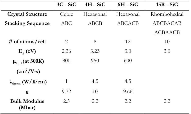
Table 2.1 Material properties of some common SiC polytypes3-8
3C - SiC 4H - SiC 6H - SiC 15R - SiC Crystal Structure Cubic Hexagonal Hexagonal Rhombohedral
Stacking Sequence ABC ABCB ABCACB ABCBACAB
ACBAACB
# of atoms/cell 2 8 12 10
Eg (eV) 2.36 3.23 3.0 3.0
μe||c(at 300K) (cm2/V·s)
800 950 600
λtherm (W/K·cm) 1 4.5 4.5
ε 9.72 10 9.66
Bulk Modulus
(Mbar) 2.5 2.2 2.2 2.2
2.1.2 Semiconductor Properties of SiC
The great potential of SiC due to its improved properties has been known for
currents. Table 2.1 below outlines various materials properties for silicon versus some common wide band gap materials.
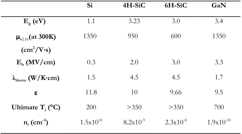
Table 2.2 Material properties comparisons of common semiconductors for power electronic devices 3-9
Si 4H-SiC 6H-SiC GaN
Eg (eV) 1.1 3.23 3.0 3.4
μe||c(at 300K) (cm2/V·s)
1350 950 600 1350
Eb (MV/cm) 0.3 2.0 3.0 3.3
λtherm (W/K·cm) 1.5 4.5 4.5 1.7
ε 11.8 10 9.66 9.5
Ultimate Tj (°C) 200 >350 >350 700
ni (cm-3) 1.5x10¹⁰ 8.2x10⁻⁹ 2.3x10⁻⁸ 1.9x10⁻¹⁰
2.2 Interface of SiC and SiO2
Similar to silicon, SiC forms a high quality SiO2 as a native oxide. From a device fabrication standpoint, this likeness has been viewed favorably as it allowed for many of the techniques developed for Si to be used on SiC.
2.1.3 Oxidation of SiC
SiC surface.10The surface areal density of the carbon controls the SiC oxidation rates due to the removal of carbon through out-diffusion of the carbonaceous species. As seen in the oxidation reaction below, oxygen is required both to form SiO2 and is needed for the out diffusion of CO:
2 SiC + 3 O2 → 2 SiO2 + 2 CO (2.1)
This results in a notably slower oxide growth rate for SiC as compared to Si at the same temperature. This also results in different oxide growth rates for different crystal faces of SiC. For MOS fabrication, SiO2 on SiC is generally grown between 1100°C and 1300°C in an oxidizing ambient. While (2.1) illustrates one oxidation reaction, there could be other reactions including:11
SiC + O2 ↔ SiO2 + C (2.2)
The carbon produced by this reaction would have to undergo an additional reaction, as shown below in (2.4), or would be left at the interface. Carbon left in the oxide would be determined by:
SiC + 2 CO ↔ SIO2 + 3 C (2.3)
2 C + O2 ↔ 2 CO (2.4)
This complex oxidation process leads to a variety of interface defects. Various methods have been studied to improve the interface quality and resulting device performance. These methods generally include pre-oxidation surface cleans, optimized oxidation conditions and post-oxidation anneals to increase electron mobility and reduce the density of interface traps.
2.1.4 Problems at the Interface of SiC and SiO2
(2.5) where τ is the mean scattering time for the speed v = μξ of a carrier in a solid. When subjected to scattering processes, the mobility of a carrier can be determined by combining the reciprocal mobilities of each scattering process.
(2.6)
Contributing scattering processes are phonon scattering, Coulomb scattering from charged centers, carrier trapping and surface roughness scattering. As the relationship explained in equation (2.6) is reciprocal, the mobility is dominated by the smallest component of τ. The dependence of the bulk mobility, μbulk, on electric field and temperature can be used to determine the dominating scattering process.12 Thus at room temperature the bulk mobility is generally limited by phonon scattering. As phonon scattering increases with electric field, the μbulk is usually taken to be the ‘low-field’ value.
The presence of interface defects and of interfacial transition layers also result in localized energy states in the band gap. In n-channel devices under gate biases high enough to cause inversion, the Fermi level nears the conduction band edge. This allows these states below the Fermi level to fill with electrons, acting as traps for the free carriers. This process is
illustrated in Fig. 2.4. This trapping reduces the carrier lifetime and also Figure 2.4 Depiction of the charge balance in a
which increase Coulombic scattering. These mechanisms cause reduced effective mobility in SiC MOSFETs. In silicon MOSFETs the effective mobility is typically 40-50% of the bulk mobility. In 6H and 4H-SiC the effective mobility, µeff, is typically about 25% and 1% of the bulk respectively. Schorner13 initially suggested that lower 4H-SiC MOSFET mobility was caused by large numbers of interfacial defects producing interface states near the conduction band of 4H-SiC. These states are neutral when empty and negatively charged when occupied by an electron and are thus referred to as ‘acceptor-like’ states. Fig.2.5 illustrates the
distribution of these states at the SiC/SiO2 interface. It is clear from Fig. 2.5 that 4H-SiC is sensitive to a larger amount of states due to the width of the 4H-SiC band gap as compared to other SiC polytypes.
In addition to surplus states due to the wide band gap of 4H-SiC, the presence of carbon at the SiC/SiO2 interface results in additional interface traps. There is no
evidence of any difference in bulk of the thermally grown SiO2 between oxide grown on Si and oxide grown on SiC. However the presence of carbon in the oxidation process due to the SiC has been shown to result in excess carbon at the SiC and SiO2 interface. This interfacial carbon has been shown in the form of an SixCyO transition layer, through a wide variety of techniques including scanning transmission electron microscopy (TEM) and electron energy loss spectroscopy (EELS),14,15,16 Rutherford backscattering (RBS),17,18,19,20 x-ray photoelectron spectroscopy (XPS), 21,22,23,24,25 and electron spin resonance (ESR).26,27While
these studies all deal with carbon at the SiC/SiO2 interface, new studies have shown the presence of defects on the SiC side of the interface. This idea of “bulk traps” or defects on the SiC side, initially introduced by Agarwal28, proposes that in addition to the acceptor-like and donor-like interface traps shown in Fig 2.5, free carriers can be lost to traps in the bulk of the SiC. Fig 2.6 shows an illustration of the band gap which has been revised to include these bulk traps. Like interface traps, bulk traps in the SiC would affect µeff, through electron trapping and Coulombic scattering. The existence of bulk traps in the SiC has been well documented.29,30,31,32,33 These traps could be caused by a variety of sources including, carbon and silicon vacancies, interstitials, impurities, carbon clusters, etc. Standard device
processing, notably implantation, high temperature annealing and thermal oxidation have all been shown to promote these defects. The defects due to high temperature oxidation of SiC have also been examined extensively using STEM and EELS.33,34,35 Hornetz used ARXPS to investigate carbon containing near- interface oxides on the Si-face of 6H-SiC in 1994.36The oxidation induced defects shown in Fig 2.6, have been shown to exist on both sides of the SiC/SiO2 interface, as oxide traps in the bulk of the SiO2, as a transition layer on the SiC side and as interface traps in between. In addition, the depth of the transition layer on the SiC side has been shown to be related to the processing and is proposed to have a relationship to the device mobility.35
Models of the SiC/SiO2 interface when paired with experimental data, have been constructive in understanding the effect of defects. Several groups have proposed models notably groups led by Pantelides37,38,39 and Deák40,41,42. The study of interfacial carbon and its related defects
remains an area of interest due to the difficulties in accurately
characterizing such low defect levels, about 1013 cm-2. While this level is low from a physical standpoint, the
electrical effects on the device are paramount. Thus complete characterization and
understanding of the defect and its effects on the band gap lies in the critical path of 4H-SiC MOSFET development.
2.1.5 Interface Passivation
As reducing the band gap of 4H-SiC is not an option, work to reduce Dit has centered around the oxidation process and post oxidation anneals (POA). Varying the oxidation process by adding Ar anneals43 or by re-oxidizing at lower temperatures44, have been demonstrated to provide a minor reduction in states deep in the band gap. Hydrogen has also been used successfully to passivate dangling Si bonds at the interface, reducing Dit in the mid-gap by an order of
Figure 2.8 Schematic of a SiC metal-oxide-semiconductor capacitor
Figure 2.7 4H-SiC interface trap densities near the conduction band for varying post oxidation
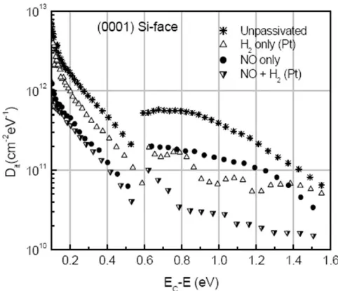
magnitude.45 However H passivation does not affect the near-interface states and as such hydrogen alone does not significantly improve device performance. In 1996, mid –gap states were shown to be reduced by the pioneering “wet reox” 950 ºC anneal process. However this mid-gap reduction had no effect on µeff. In 1997, POA in nitric oxide (NO) at the high temperature of 1100ºC was shown to reduce Dit in 6H-SiC MOS systems.47 Similar positive results were demonstrated for SiO2/4H-SiC interfaces using both NO44,47and N2O.48 With NO anneals trap densities near the conduction band have been reduced from ~ 1013 cm-2eV-1 to ~1012 cm-2eV-1, as shown in Fig. 2.7. This reduction in near-interface states has led device mobilities approaching 60 cm2V-1s-1.50,51,52 These mobility values have designated NO anneals as an essential processing step for the fabrication of SiC MOSFETs for both
scientific and industrial applications. While the benefits of NO anneals have been ascribed to bonding of nitrogen at the interface, the kinetics of the process are still under
investigation.Exposure to NO at high temperatures has been shown to reduce the amount of excess carbon at the interface through both AFM53, which shown a smoother surface post anneal and through XPS54. XPS studies have revealed both a reduction in C containing compounds at the interfaces, as well as formation of Si-N and C-N bonds. These studies have encouraged the notion that nitrogen is either operating via two possible paths: nitrogen binding at defect sites/dangling bonds
or through nitrogen substitution for a three-fold C or Si. However the mobility of SiO2/4H-SiC interface as a percentage of the bulk mobility is still low compared to silicon. Additional improvements must be made to the interface in order to determine the maximum inversion mobility of 4H-SiC MOS systems.
The alternate faces of SiC,
face and C-face, have also been investigated for increased mobility. Both faces have great potential for development with increased oxidation rates as well as improved mobility over the commonly used Si-face. However the relationship between increased oxidation rates and carbon related defects requires further investigation. Deposited oxides, notably low
temperature PECVD oxides, have also been studied in the past decade but have not shown benefits over thermally oxidized samples.55,56 Low temperature deposition is desired as a means of avoiding any defect creation from the high temperature thermal oxidation. However PECVD oxides have not shown any improvement over thermally grown oxides, perhaps related to the plasma damage imparted to the gate oxide through this deposition technique. As such a low temperature technique that does not involve exposure to plasma, such as atomic layer deposition, is an ideal candidate for evaluation.
2.3 SiC MOSFETs
As discussed previously, the ability of SiC to form SiO2 as its native oxide is an
advantage when comparing SiC to other wide band-gap materials. The deposition of a metal onto this native oxide results in the formation of a metal-oxide-semiconductor (MOS)
capacitor. MOS capacitors, as shown in Fig.2.8, are valuable test devices that also form the functional core of the
metal-oxide-semiconductor field effect transistor (MOSFET). The relationship between the energy levels of the metal (assuming Al), oxide and semiconductor is shown in Fig 2.9. This figure shows an ideal system with no states in the gap. Actual devices are far from perfect and contain numerous states in the gap as discussed in the previous sections.
MOSFETs are four terminal transistors used for switching or amplification of small signals. They are the most common transistor used in digital or analog circuits. To operate a MOSFET a potential is applied to a gate electrode to regulate the flow of minority carriers from the source to the drain. This turns the device off and on or can be used to amplify signals.57 MOSFETs are typically fabricated with highly doped contacts in a lightly doped substrate, a gate oxide and contacts. Figure 2.10 illustrates a simple four terminal MOSFET. MOSFETs can be fabricated to be enhancement or depletion mode devices with an n-type or p-type channel. Enhancement mode devices are normally off and exhibit negligible current flow with zero volts on the gate while depletion mode devices are normally on and require reverse biased gates to turn off the device.The following MOSFET descriptions will be based on an n-channel MOSFET as seen in fig. 2.10.
2.3.1 MOSFET Operation
As described above the operation of the MOSFET is controlled by applying a positive or negative voltage to the gate electrode. With no voltage applied to the gate the Fermi levels of the metal,
oxide and semiconductor align assuming no fixed oxide charges, interface states and work function difference between metal and SiC. This is considered equilibrium or flat band condition. Figure 2.11 shows the operation modes of an n-channel MOSFET. Schematic a show the flat
band condition with all Fermi levels aligned. The application of a negative gate voltage results in hole accumulation at the oxide/semiconductor interface. As seen in Fig 2.11b this causes upward band bending.
When a positive voltage is applied from the gate electrode to the body, VGB, the positively charged holes are repelled away from the oxide/semiconductor interface forming a depletion region. This region filled with negatively charged acceptor ions accounts for the negative charge at the semiconductor surface. As seen in Fig 2.11c, the bands in this region bend downward to bring Ei closer to EF. A schematic of a depletion region in a MOSFET can be seen in Fig 2.12. When VGB is sufficiently positive, the large positive gate potential attracts free electrons to the surface and creates an inversion layer, or channel. In this channel region Ei is below EF as show in Fig. 2.11d. A schematic depicting a MOSFET with an inversion channel can be seen in Fig 2.12. The extremely large electron concentration results in an n-type
conducting layer. The minimum gate voltage required for channel formation is called the threshold voltage, Vth. Although inversion layers are formed when φs is greater than φF, a true conducting channel only exists under strong inversion (φs≥ 2φF).
2.3.2 MOSFET Characteristics
MOSFETs are generally tested by applying a variable gate voltage and examining the relationship between the drain current and the drain to source voltage. This typical
measurement, generally referred to as the family of curves, can be seen in Fig. 2.13. Current saturation can occur at all applied gate voltages and is shown in the saturation region. The
point at which current saturation begins, or the pinch-off voltage, is where the resistance of the channel is too great to move additional carriers through the channel. This relationship is expressed as:57
(2.7)
where W and L are the depletion region width and length, Cox is the oxide
capacitance and VG is the gate bias. Thus the saturation current is dependent on the effective mobility, oxide capacitance and threshold voltage all of which can be engineered to change device characteristics.
The MOS structure is also often evaluated using capacitance-voltage, C-V, measurements. A sample C-V curve illustrating the three regions of operation is shown below in Fig. 2.14. C-V
measurements are performed by sweeping the gate voltage and monitoring the capacitance. These measurements can be taken at high frequencies (> 1MHz) or at low frequencies (between 1-100Hz). At high frequencies, carriers in the inversion layer do not have time to respond to the rapidly changing gate voltage. Unlike in a
Figure 2.13 Typical MOSFET family of curves showing Id-Vds behavior for varying gate voltages.58
MOSFET with source and drain regions, within a MOS capacitor, the electron concentration is determined by the slow process of thermal generation and recombination. Thus in strong inversion at high frequencies, there is no electron contribution to the capacitance and the capacitance is at a minimum, Cmin. At low frequencies, there is ample time for minority carrier generation in the bulk and carriers can move into the inversion layer or recombine in the bulk of the substrate. Operation in the accumulation region does not vary with frequency due to the faster response of the majority carriers.
The relationship between the capacitance and the charge at the semiconductor surface for all regions is defined as:61
(2.8)
where Qs is the surface charge. The total capacitance can be written as the sum of the oxide capacitance and the semiconductor capacitance as shown below.7
(2.9)
2.3.3 Oxide and Interface Charge
Thus far, explanations of MOS capacitor and MOSFET operation have assumed an ideal MOS system with no imperfections. Unfortunately the semiconductor, oxide and metal all have intrinsic imperfections. There are four major sources of charge at the
oxide/semiconductor interface and in the oxide that can affect MOS performance. These charges are illustrated in Fig. 2.15. The four major charges include: interface trap charge, oxide fixed charge, oxide trapped charge and mobile ionic charge. Interface trap charges, as
discussed in the previous sections, are present at the oxide/semiconductor interface due to defects at the interface. These defects can include dangling bonds from the termination of the crystal lattice or residual carbaceous species from the oxidation of the semiconductor. Interface traps can trade mobile carriers with the substrate, acting as donors or acceptors
depending on the trapped carrier. Fixed charges in the oxide are generally located near the transition region on the oxide side of the interface. These charges are the created by the oxide formation process and are not related to oxide thickness. Oxide trapped charges generally found at the oxide interfaces with the gate or semiconductor. These are most commonly a consequence of oxide imperfections, ionizing radiation, high-energy carrier injection via avalanche or tunneling from the surface. Lastly mobile ionic charges are the result of contaminates introduced through device processing. The mobile nature of the ions means that they move freely in the oxide under the presence of an electric field and thus are easily screened for. A clean process environment, high grade consumables and proper wafer handling greatly reduce the likelihood of mobile contamination.
Figure 2.15 The four types of charges, labeled by color, in the MOS system.12
The primary bulk electron trap in SiO2 is reported to be related to water, as the trap density scales with vapor pressure during gate oxide growth.45,62 These traps are neutral but become negatively charges after electron capture. The negative charge is not removed by photo-excitation after capture. This suggests that the trapping mechanism is an electro-chemical reaction that changes the local oxide structure. For holes, excess positive charge appears most stable close to the SiO2 interfaces the metal and semiconductor.18 This positive charged region near the interface is enhanced in nitrided SiO2 on silicon.63-68 In nitrided SiO
2 grown on SiC, the hole trap density has been reported to scale with the nitrogen
concentration at the oxide/semiconductor interface.69 It is expected that an SiO xNy transition region would result in hole traps as the band-gap of Si3N4 falls within the SiO2 band-gap.70 Calculations have shown that nitrogen provides a lone pair of electrons in Si-N-Si or Si-N-Si-NO-Si-N-Si configurations that can capture a hole.69 While research has shed light on the effects of excess carriers in the SiO2 and provided several possible models, the specifics associated with charge trapping and interface state generation on the atomic-scale are still unclear.
2.3.4 Non-Ideal Charge effect on I-V Characteristics
As these added charges do not balance out, the ideal flatband condition, seen in Fig. 2.11, is only achieved by applying a bias to the device. This shifts the whole C-V curve by the amount necessary to overcome the oxide charge. Since the threshold voltage is defined as the onset of strong inversion, then the VT is also shifted. The additional oxide charges are included in the calculation of the threshold voltage as:61
(2.10)
where ΦMS is the work function potential difference between the gate and the
threshold is symptomatic of a normally-on device, while a positive threshold indicates an enhancement-mode device.
Non-ideal oxides also exhibit electric field dependant conduction of gate leakage current. As the device ages during normal operation, charges are built up in the gate dielectric and interface states are generated. These processes and the associated leakage currents can result in reduced inversion layer mobility, threshold voltage instabilities and the ultimate breakdown of the gate dielectric. Excess carriers in the dielectric are impossible to avoid due to low and high field injection and tunneling mechanisms including: thermionic emission, Fowler-Nordheim tunneling, Frenkel-Poole emission, trap assisted tunneling and direct tunneling.
As shown in Figure 2.9, the 4H-SiC/SiO2 conduction band offset is about 2.7eV, which should be enough to provide a barrier to thermionic excitation of carriers through the oxide layer. The current due to thermionic emission is given by:71
(2.11)
where A* is the effective Richardson constant for thermionic emission in Acm-2K-2. For free electrons A is 120 Acm-2K-2 and for SiC A* ≈ 2.1 x A.71, 72From the equation for current density due to thermal emission one can verify that under temperatures of 600 ºC or greater, currents due to thermionic emission areinsignificant.
Fowler-Nordheim (F-N) occurs at high enough oxide fields, where carriers from the metal or semiconductor can tunnel through a portion of the oxide. The triangular barrier related to F-N injection can be seen in Fig. 2.16. This tunneling results in an intrinsic leakage current, JFN. The tunneling current density can be expressed as:73
(2.12)
Frenkel-Poole (F-P) emission is commonly seen at high temperature and high fields. It is due to emission of carriers from the localized states within the oxide. The presence of an electric field modifies the potential energy profile such that the work required to free a trapped carrier is reduced. The current density for Frenkel-Poole emission is given by:71
(2.13)
Like thermionic emission, Frenkel-Poole emission is driven by thermal emission. However there are differences, including that carriers process by drift conduction in F-P emission and
that F-P is defect-mediated and thus extrinsic.
Trap assisted tunneling occurs through defects in the oxide. These traps act as stepping stones for charge carriers. This process is also referred to as stress-induced leakage currents when the traps are formed through prolonged exposure to high electric fields. For both processes the limiting step of the
process is tunneling from the traps to the conduction band. Thus reducing the number of traps available is critical to deterring this type of tunneling.
Direct tunneling occurs when electrons from the metal or semiconductor can tunnel through the gate oxide without going through the conduction band. Oxide thickness and dielectric constant can be varied to increase the barrier and reduce direct tunneling. The use of high-k dielectrics has allowed for similar effective oxide thicknesses to be achieved with physically thinner oxides.
2.3.5 Non-Ideal Charge Effect on C-V Characteristics
The addition of non-ideal charges increase the density of interface states as previously discussed. C-V measurements are often used to investigate Dit as trap response changes with frequency and bias. Traps can change their charge state quickly to respond to varying gate biases, moving above or below the Fermi level. States below the Fermi level are more likely to be occupied than those above. As the bias changes, traps above the Fermi level give up their electrons to the semiconductor, while those below the Fermi level will trap electrons from the semiconductor. Further discussion of the affect of interface traps on C-V measurement is provided in Chapter 3.
2.4 Summary
2.5 References
1. M. Shur, S. Rumyantsev and M. Levinshtein, SiC Materials and Devices, Volume 2. (World Scientific, Hackensak, NJ, 2007).
2. K. Jarrendahl and R. F. Davis, SiC Materials and Devices. (Academic Press, London, 1998).
3. Materials properties taken from
http://www.ioffe.rssi.ru/SVA/NSM/Semicond/index.html (April 2012). 4. W.Y. Ching, Y.-N. Xu, P. Rulis, and L. Ouyang. Materials Science and Engineering A.
422, 147 (2003).
5. G. Wellenhofer and W. Rossler. Solid State Communications. 96, 11 (1995) 887-891. 6. T.P. Chow. Microelect. Eng. 83,112(2006).
7. S.J. Pearton, C.R. Abernathy, M.E. Overberg, G.T. Thaler, A.H. Ostine, B.P. Gila, F. Ren, B. Lou, and J. Kim. MaterialsToday,24(Jun. 2002).
8. D.C. Look, J.R. Sizelove. Applied Physics Letters79, 1133(2001).
9. G. Pensl and W. J. Choyke, Physica B: Physics of Condensed Matter 85, 1 (1993).
10. Y. Song and F. W. Smith, Applied Phyics Letters81, 3061 (2002). 11. C. I. Harris and V. V. Afanas’ev, Microelectr. Eng. 36, 167 (1997).
12. R. Muller and T. Kamins, Device Electronics for Integrated Circuits. (Wiley New York,
2003).
13. R. Schorner, P. Friedrichs, D. Peters, and D. Stephani, IEEE Electron Device Lett. 20, 241 (1999).
14. K. C. Chang, N. T. Nuhfer, L. M. Porter, and Q. Wahab, Applied Physics
Letters 77, 2186 (2000).
15. K. C. Chang, L. M. Porter, J. Bentley, C. Y. Lu, and J. Cooper, J., Journal of Applied Physics 95, 8252 (2004).
17. S. Dhar, Y. W. Song, L. C. Feldman, T. Isaacs-Smith, C. C. Tin, J. R. Williams, G. Chung, T. Nishimura, D. Starodub, T. Gustafsson, and E. Garfunkel, Applied Physics Letters 84, 1498 (2004).
18. T. Okawa, R. Fukuyama, Y. Hoshino, T. Nishimura, and Y. Kido, Surface Science 601, 706 (2007).
19. D. J. Hayton, T. E. Jenkins, P. Bailey, and T. C. Q. Noakes, Semiconductor Science and Technology 17, L29 (2002).
20. C. Radtke, I. J. R. Baumvol, and F. C. Stedile, Physical Review B 66, 155437 (2002). 21. A. Ekoue, O. Renault, T. Billon, L. Di Cioccio, and G. Guillot, MaterialsScience Forum
433, 555 (2003).
22. C. Virojanadara and L. I. Joahnsson, Surface Science 505, 358 (2002).
23. C. Virojanadra and L. I. Johansson, Journal of Physics: Condensed Matter 16,1783 (2004). 24. B. Hornetz, H.-J. Michel, and J. Halbritter, Journal of Materials Research 9,3088 (1994). 25. G. G. Jernigan, R. E. Stahlbush, and N. S. Saks, Applied Physics Letters 77,1437
(2000).
26. J. L. Cantin, H. J. von Bardeleben, Y. Shishkin, Y. Ke, R. P. Devaty, and W. J. Choyke, Physical Review Letters 92, 15502 (2004).
27. J. L. Cantin and H. J. von Bardeleben, Materials Science Forum 527, 1015 (2006). 28. A. Agarwal and S. Haney, Journal of Electronic Materials 37, 5 (2008).
29. W.J.Choyke and R.P. Devaty, Silicon Carbide—RecentMajorAdvances, ed. W.J. Choyke, H. Matsunami and G. Pensl (New York: Springer-Verlag, 2003), p. 413. 30. N. Achtziger and W. Witthuhn, Silicon Carbide—RecentMajor Advances, ed. W.J.
Choyke, H.Matsunami and G. Pensl (New York: Springer-Verlag, 2003), p. 537. 31. M.O. Aboelfotoh and J.P. Doyle, Phys. Rev. B 59, 10823 (1999).
32. S. Mitra, M.V. Rao, N. Papanicolaou, K.A. Jones, M. Derenge, O.W. Holland, R.D. Vispute, and S.R. Wilson, J. Appl. Phys. 95, 69 (2004).
34. T. Zheleva, A. Lelis, G. Duscher, F. Liu, I. Levin and M. Das, Applied Physics Letters
93,022108 (2008).
35. Trinity Biggerstaff, Ph.D. Thesis, North Carolina State University, 2008. 36. B. Hornetz, Journal of Vacuum Science & Technology A, 13, 3 (1995).
37. S. Wang, M. Di Ventra, S. G. Kim, and S. T. Pantelides, Physical Review Letters 86, 5946 (2001).
38. S. T. Pantelides, S. Wang, A. Franceschetti, R. Buczko, M. Di Ventra,S. N.
Raashkeev, L. Tsetseris, M. H. Evans, I. G. Batyrev, L. C. Feldman,et al., Materials Science Forum 527, 935 (2006).
39. S. Wang, S. Dhar, S.-r. Wang, A. C. Ahyi, A. Franceschetti, J. R. Williams,L. C. Feldman, and S. T. Pantelides, Physical Review Letters 98, 026101 (2007).
40. J. M. Knaup, P. Deák, T. Frauenheim, A. Gali, Z. Hajnal, and W. J. Choyke,Physical Review B 71, 235321 (2005).
41. P. Deák, T. Hornos, C. Thill, J. M. Knaup, A. Gali, and T. Frauenheim, Materials Science Forum 556-557, 541 (2007).
42. P. Deák, J. M. Knaup, T. Hornos, C. Thill, A. Gali, and T. Frauenheim, Journal of Physisics D: Applied Physics 40, 6242 (2007).
43. E. G. S. von Kamienski, F. Portheine, J. Stein, A. Golz, and H. Kurz, Journal of Applied Physics 79, 2529 (1996).
44. G. Y. Chung, C. C. Tin, J. R. Williams, K. McDonald, M. D. Ventra, S. T. Pantelides, L. C. Feldman, and R. A. Weller, Applied Physics Letters 76, 1713 (2000).
45. E. H. Nicollian and J. R. Brews:MOS (Metal Oxide Semiconductor) physics and technology
(John Wiley & Sons, New York, 1982).
46. L.A. Lipkin and J.W. Palmour, J. Electron. Mater. 25, 909(1996).
47. H.-F. Li, S. Dimitrijev, H. B. Harrison, and D. Sweatman, Appl. Phys. Lett. 70, 2028 (1997).
49. S. Wang, S. Dhar, S.-r. Wang, A. C. Ahyi, A. Franceschetti, J. R. Williams, L. C. Feldman, and S. T. Pantelides, Physical Review Letters 98, 026101 (2007).
50. G. Y. Chung, C. C. Tin, J. R. Williams, K. McDonald, R. K. Chanana, R. A. Weller, S. T. Pantelides, L. C. Feldman, O. W. Holland, M. K. Das, and J. W. Palmour,
IEEE Electron Device Lett. 22, 176 (2001).
51. M. K. Das, Materials Sci. Forum 457, 1275 (2004).
52. C.-Y. Lu, J. A. Cooper Jr, T. Tsuji, G. Chung, J. R. Williams, K. McDonald, and L. C. Feldman, IEEE Trans. Electron Devices 50, 1582 (2003).
53. S. Dimitrijev, H. B. Harrison, P. Tanner, K. Y. Cheong, and J. Han. SiliconCarbide: Recent Major Advances, pp. 373–386 (Springer, 2004).
54. H. Li, S. Dimitrijev, D. Sweatman, H. B. Harrison, P. Tanner, and B. Feil,Journal of Applied Physics 86, 4316 (1999).
55. Masato Noborio, Ph.D. Thesis, Kyoto University, 2009.
56. P. Mandracci, S. Ferrero, C. Ricciardi, L. Scaltrito, G. Richieri and C. Sgorlon, Thin Solid Films, 427 (2003).
57. Y. Tsividis. Operation and Modeling of the MOS Transistor (2nd Edition). (McGraw Hill, Boston 1999).
58. W. Lu, L. C. Feldman, Y. Song, S. Dhar, W. E. Collins, W. C. Mitchel, and J. R. Williams, Appl. Phys. Lett. 85, 3495 (2004).
59. V. V.Afanas’ev, M. Bassler, G. Pensl, M. J. Schulz, and E. S. von Kamienski, J. App. Phys.l 79, 3108 (1996).
60. Image retrieved from http://en.wikipedia.org/wiki/File:IvsV_mosfet.svg (May 2012).
61. B. Streetman and S.K. Banerjee. Solid State Electronic Devices. (Prentice Hall, New Jersey 2006).
62. E. H. Nicollian, C. N. Berglund, P. F. Schmidt, and J. M. Andrews, Journal of Applied Physics 42, 5654 (2003).
64. A. E. Islam, H. Kufluoglu, D. Varghese, S. Mahapatra, and M. A. Alam,IEEE Transactions on Electron Devices 54, 2143 (2007).
65. J. B. Yang, T. P. Chen, S. S. Tan, C. M. Ng, and L. Chan, Journal of the Electrochemical Society 154, G255 (2007).
66. S. S. Tan, T. P. Chen, C. H. Ang, and L. Chan, Microelectronics Reliability 45, 19 (2005). 67. A. E. Islam, G. Gupta, S. Mahapatra, A. T. Krishnan, K. Ahmed, F. Nouri,A.
Oates, and M. A. Alam, Proceedings of the International Electron Devices Meeting, (2006). 68. T. Sasaki, K. Kuwazawa, K. Tanaka, J. Kato, and D.-L. Kwong, IEEE Electron
Device Letter 24, 150 (2003).
69. John Rozen, Ph.D. Thesis, Vanderbilt University, 2008.
70. K. Muraoka, K. Kurihara, N. Yasuda, and H. Satake, Journal of Applied Physics 94, 2038 (2003).
71. S. M. Sze, Semiconductor Devices, Physics and Technology (Wiley, New York 1981).
72. C. F. Pirri, S. Ferrero, L. Scaltrito, D. Perrone, S. Guastella, M. Furno, G. Richieri, and L. Merlin, Microelectronic Engineering 83, 86 (2006).
C H A P T E R 3
RESEARCH METHODOLOGY
3.1 Atomic Layer Deposition
Atomic layer deposition (ALD) was first introduced by Suntola and co-workers in the late 1970s as atomic layer epitaxy (ALE).1 It was initially presented as a new technique to deposit amorphous and polycrystalline thin films. In the decades since its introduction ALD has become a technique of great interest due to its many benefits. The primary benefits include complete control over the deposition process and ability to achieve conformal pin-hole free coatings even in high aspect ratio and complex structures.
ALD growth chemical gas phase process is based on alternative, self – limiting surface saturating reactions. A monolayer of precursor saturates the surface with each exposure step. The simplest ALD cycle is based on the following four step sequence:
1) Exposure of the first precursor, precursor A, resulting in a reaction of the surface with precursor A
2) Purge of non-reacted precursor A and gaseous reaction by-products through gas flow or evacuation of the process chamber
3) Exposure and self-terminating reaction of the second precursor, precursor B 4) Purge or evacuation
excess precursor is purged or evacuated. The second
precursor (the blue symbols) is pulsed into the chamber and begins to react in drawing d. Finally when the self-limiting reaction is complete the excess precursor is again purged and the reaction cycle can begin again. In each of these chemical reactions the entire surface reacts to complete saturation, ensuring that other reactions do not occur. This self – limiting feature directly leads to a number of
advantages of ALD including:
Easy and precise thickness control
Exceptional conformality, even with complex structures and high aspect ratios High quality films even at low process temperatures
Good reproducibility
Ability to vary deposited film materials or create multilayer structures in situ Ability to achieve sharp interfaces between films
In an ALD process, a plot of the growth rate versus substrate temperature is often used to determine the optimal processing region. These plots show the “ALD process window” as a flat plateau region where self-limiting reaction takes place. An example of these plots can be seen below in Fig. 3.2. This figure clearly illustrates how temperature is the most important parameter in controlling the saturation mechanism. If low growth rates are observed, temperatures could be too low to achieve the required activation energy for the reaction or temperatures could be so high that the monolayer of precursor is desorbing from the surface. Low temperatures with high growth rates indicate condensation of the precursor on the surface. Finally when temperatures are too high, the precursor can
decompose on the surface thus prohibiting self-limited growth.
ALD processes are performed in a flow reactor. The main inert gas flow feeds reactants into the process chamber. Figure 3.2 The ALD process window as related to growth rate