http://www.scirp.org/journal/mnsms ISSN Online: 2164-5353
ISSN Print: 2164-5345
DOI: 10.4236/mnsms.2017.73003 Jul. 30, 2017 33 Modeling and Numerical Simulation of Material Science
Numerical Simulation of Varied Buffer Layer of
Solar Cells Based on Cigs
Sampson Oladapo Oyedele, Boko Aka
*Université Nangui Abrogoua, UFR des Sciences Fondamentales et Appliquées (SFA) et Institut de Recherche sur les Energies Nouvelles (IREN), Abidjan, Côte d’Ivoire
Abstract
Numerical simulation has been used to investigate the effect of different buffer layer components on the performance of CuInGaSe2 solar cells with SCAPS-1D
software. The main photovoltaic parameters of simulated devices: open-circuit voltage (Voc), short-circuit current (Jsc), fill factor (FF), and conversion efficiency (η), are analysed as a function of thickness and temperature in the different
buffer layers used. According to numerical simulation the highest conversion efficiency (23%) of CIGS solar cell is reached for the CdS buffer layer. This re-sult is validated by experimental rere-sults (20%). At 300 K, when the thickness of the buffer layer (CdS, ZnS, ZnSe, InSe2) increases from 100 nm to 500 nm, with
the other parameters maintained constant, the efficiency decreases. When the temperature increases from 300 K to 400 K, with the other parameters maintained constant, both open circuit voltage and conversion efficiency also decrease. The effect of dual buffer layers of ZnS/CdS has also been analysed and his efficiency increases of 3% than a single buffer CdS.
Keywords
Numerical Simulation, CIGS Solar Cell, SCAPS-1D, Buffer Layer, Efficiency
1. Introduction
The growth of the world’s population and industrial development of industria-lized countries is leading to an increase in energy need. Worldwide, current energy production is mainly based on fossil fuels but it pollutes the environment and raises the relative proportion of greenhouse gases in the atmosphere. The detrimen-tal effects of non-renewable resources on our environment have led to a greater awareness generating the conference of PARIS [1]. This conference of PARIS en-couraged the use of renewable energies like photovoltaic energy. Solar energy can
How to cite this paper: Oyedele, S.O. and Aka, B. (2017) Numerical Simulation of Varied Buffer Layer of Solar Cells Based on Cigs. Modeling and Numerical Simulation of Material Science, 7, 33-45.
https://doi.org/10.4236/mnsms.2017.73003
Received: June 17, 2017 Accepted: July 27, 2017 Published: July 30, 2017
Copyright © 2017 by authors and Scientific Research Publishing Inc. This work is licensed under the Creative Commons Attribution International License (CC BY 4.0).
http://creativecommons.org/licenses/by/4.0/
DOI: 10.4236/mnsms.2017.73003 34 Modeling and Numerical Simulation of Material Science
be harvested with photovoltaic (PV) cells solar-cells.
The CIGS solar cell is one of the promising solar cells. The efficiency of CIGS is up to 23% [2] one of the best efficiency of a thin film. The CIGS solar cell has also many merits. It has a variable band gap (from 1.06 eV to 1.7 eV) and has also a high optical absorption coefficient and a direct band gap. The solar cell is com-monly used with a configuration of “glass/Mo/CIGS/buffer/i-ZnO/transparent con-ductive oxide (TCO)”. On CIGS solar cell structure, the buffer layer intermediates between the absorber layer and window layer. It improves generally the cell effi-ciency and has many tasks:
Forms a junction with the absorber layer while admitting a maximum amount
of light to the junction region and absorber layer [3];
Provides a low resistive path to contacts;
Fixes the electrostatic conditions inside the absorber layer [4];
Protects the junction electrically and mechanically against the damage that may other side be caused by oxide.
From the electronic point of view, since buffer layers are usually highly-resistive, they serve as intermediate layers that can prevent shunting between the TCO and the absorber [5].
From the technological point of view, buffer-layers can protect the absorber surface from damage by high-energy ions during the n+ZnO deposition by RF-sputtering.
From the chemistry point of view, chemical constituents of buffer material passiv-ize CIGS surface defects and/or dope the CIGS near-surface layer.
And finally, from the physics point of view, buffer layers affect the band struc-ture. Buffer layers affect the band offsets and also the electric field in the junction, and thus the current transport [6]. It has proved that omitted the buffer layer re-sult in lower efficiency [7].
So, we need to choose carefully the buffer layer to improve the device perfor-mance. The material must obey to this criterion. The requirements are listed be-low:
This layer should have minimal absorption losses;
Large energy band gap for high optical transmission in the visible region;
An optimum band structure;
The juxtaposition of crystal structures at the junction must be great so as to
generate the fewest defects (and thus recombination centers) possible during the growth of the buffer layer; for the same reasons, the compound should be stable over time;
The n-doping of the buffer layer should ideally be higher than that of the
ab-sorber so as to confine the Space Charge Region (SCR) in the abab-sorber; high doping density is also necessary to prevent the generation of minority carri-ers, thereby reducing the reverse current, however, too high a doping could al-so cause a recombination tunnel current to the interface in the case of a high band discontinuity;
The process and material choice of the buffer layer should provide an
DOI: 10.4236/mnsms.2017.73003 35 Modeling and Numerical Simulation of Material Science
conduction of 0 - 0.4 eV.
The buffer usually used for CIGS solar cell is CdS but due to the toxicity of cadmium sulfide (CdS) many countries have prohibited the cadmium sulfide (CdS) and also due to a low band gap of CdS (2.4 eV), only a lower fraction of photons are available for CIGS absorber this leads to loss of current in the blue region of the solar spectrum and hence limits the solar cell performance; serious efforts have been made to substitute the CdS buffer by other non-toxicity layer like CIGS based thin film can be a mark. To change the CdS:
The material should be n-type in order to form a p-n junction with the ab-sorber layer;
The bandgap should be wide for limited light absorption;
A wide band gap, greater than that of CdS, in order to transmit a maximum
of photons to the absorber.
So in this work, we use different buffer layers and by simulation with SCAPS1-D [8], we discuss their effects in the CIGS base cell performances. We also studied the impact of buffer thickness and effect of variable temperature on PV performance. In order to improve the efficiency of CIGS based cell, we use the dual buffer and we studied their effect on photovoltaic (PV) parameters.
2. Methodology
2.1. Cell Structure
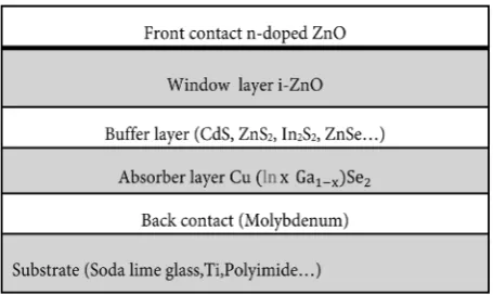
The photovoltaic structure to be studied is based on CIGS absorber with alterna-tive buffer layer as ZnO as window layer and front contact Molybdenum (Mo) taken as front contact. This used configuration for a CIGS solar cell as shown in Fig-ure 1.
2.2. Input Parameters
[image:3.595.260.488.570.706.2]In order to run numerical simulation calculations, the baseline parameters of all the components of the solar cell have to be defined to be used as inputs for SCAPS software. Theses parameters can be grouped in two sets: parameters for CIGS solar cell and parameters for variable buffer layers. The thickness of CIGS is two (2) µm and we varied the thickness of the varied buffer (CdS, ZnS, ZnSe,
DOI: 10.4236/mnsms.2017.73003 36 Modeling and Numerical Simulation of Material Science
In2S2) from 0.1 µm to 0.5 µm and the temperature of solar cell from 300 K to 400
K. All these materials are well known materials and their properties can be easily found in the literature and experimental studies available in the references [9]. The structure has been studied under solar spectrum AM 1.5 with P = 1000 W/m2 and
at a temperature T = 300 K. The simulation of the photovoltaic parameters has been made without considering the influences of the series and shunt resistance (Table 1).
3. Results and Discussion
3.1. Simulation of Solar Cell by Changing the Buffer Layer
Materials
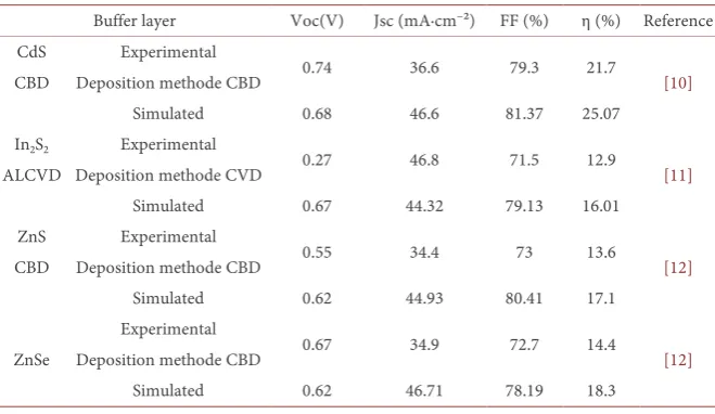
[image:4.595.208.538.315.503.2]We simulated a varied buffer layer with a thickness of 0.1 µm and we compared the main photovoltaic (PV) parameters for both simulated and experimental da-ta (Table 2).
Table 1. Physical parameters used in simulation.
CIGS CdS ZnS ZnSe In2S2
Thickness (µm) 2 varied Varied Varied varied
Band gap (eV) 1.2 2.400 3.500 2.900 2.800
Electron affinity (eV) 4.5 4.500 4.500 4.090 4.700
Dielectric permittivity (relative) 13.6 10.000 10.000 10.000 13.500
CB density of state (cm−3) 2 × ×1018 1.5 × 10¹⁸ 1.5 × 10¹⁸ 1.5 × 10¹⁸ 1.8 × 10¹⁹
VB density of state (cm−3) 1.5 × 10¹⁹ 1.8 × 10¹⁸ 1.8 × 10¹⁸ 1.8 × 10¹⁹ 4.0 × 10¹³
µn electron mobility (cm2/Vs) 100 50 50 50 400
µh hole mobility (cm²/Vs) 12.25 20 20 20 210
Donor density ND (cm−3) 1 × 10¹⁶ 0 0 0 10
Acceptor density NA (cm−3) 0 1 × 10¹⁷ 1 × 10¹⁷ 5.5 × 10⁷ 1.0 × 10¹⁸
Electron thermal velocity (cm/s) 3.9 × 10⁷ 1.0 × 10⁷ 1 × 10⁷ 1.0 × 10⁷ 1.0 × 10⁷
Hole thermal velocity (cm/s) 1.4 × 10⁷ 1.0 × 10⁷ 1 × 10⁷ 1.0 × 10⁷ 1.0 × 10⁷
Table 2. Comparison between simulation results with experimental data.
Buffer layer Voc(V) Jsc (mA∙cm−²) FF (%) η (%) Reference
CdS Experimental
0.74 36.6 79.3 21.7
CBD Deposition methode CBD [10]
Simulated 0.68 46.6 81.37 25.07
In2S2 Experimental
0.27 46.8 71.5 12.9
ALCVD Deposition methode CVD [11]
Simulated 0.67 44.32 79.13 16.01
ZnS Experimental
0.55 34.4 73 13.6
CBD Deposition methode CBD [12]
Simulated 0.62 44.93 80.41 17.1
ZnSe
Experimental
0.67 34.9 72.7 14.4
Deposition methode CBD [12]
[image:4.595.208.538.533.724.2]DOI: 10.4236/mnsms.2017.73003 37 Modeling and Numerical Simulation of Material Science
The conversion efficiency of the simulated CIGS cell is quite close to the expe-rimental result obtained from the real device. The best efficiency is obtained for CdS buffer layer.
3.2. Effect of
Various
Thickness of Different Buffer Layers
(CdS, ZnSe, ZnSe,
In
2S
2)
In order to check the effect of various thickness on CIGS photovoltaic parame-ters (PV), we varied thickness of various buffer layers from 0.1 µm to 0.5 µm while keeping constant the thickness of the window and absorber layer.
3.2.1. Effect of Various Thickness of CdS
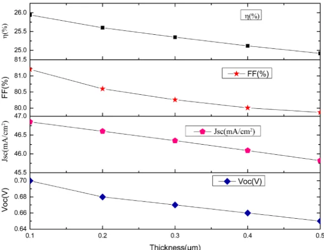
Figure 2 shows a simulated various thickness of CdS buffer layer and shows the main photovoltaic parameters Voc, Jsc, FF and η. In this simulation, the thick-ness of CdS is varied from 0.1 µm to 0.5 µm. As the thickthick-ness of CdS buffer layer is increased, the Jsc has declined from 46.9 mA∙cm−2 to 46.6 mA∙cm−2 therefore a
decrease of 7% and from 0.1 µm to 0.5 µm, Voc decreases of 7%. FF decreases from 81.1% to 78.8% therefore a decrease of 3%.
[image:5.595.212.534.454.702.2]3.2.2. Effect of Various Thickness of ZnS
Figure 3 presents a simulated various thickness of ZnS buffer layer and shows the main photovoltaic parameters Voc, Jsc, FF and η. In this simulation, the thickness of ZnS is varied from 0.1 µm to 0.5 µm. The Jsc has declined from 46.04 mA∙cm−2 to 45.75 mA∙cm−2 therefore a decrease of 7%. F.F drops from
81.57% to 72.11% therefore a decrease of 12%. η drops from 25.59% to 25.39% therefore a decrease of 8%. From 0.1 µm to 0.2 µm Voc remains constant at 0.68
DOI: 10.4236/mnsms.2017.73003 38 Modeling and Numerical Simulation of Material Science
Volt and from 0.2 µm to 0.5 µm Voc increase from 0.68 V to 0.76 V therefore an increase of 12%.
[image:6.595.211.537.211.456.2]3.2.3. Effect of Various Thickness of ZnSe
Figure 4 shows a simulated various thickness of ZnSe buffer layer and shows the main photovoltaic parameters Voc, Jsc, FF and η. In this simulation, the thick-ness of ZnSe is varied from 0.1 µm to 0.5 µm. As the thickthick-ness of ZnSe buffer layer is increased, the Jsc is declined from 46.83 mA∙cm−2 to 46.07 mA∙cm−2
[image:6.595.209.539.226.692.2] [image:6.595.210.536.471.704.2]therefore a decrease of 2%. Voc remain the same.
Figure 3. Effect of various thickness of ZnS.
DOI: 10.4236/mnsms.2017.73003 39 Modeling and Numerical Simulation of Material Science
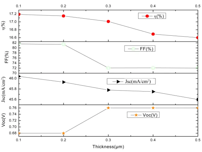
[image:7.595.217.531.471.711.2]3.2.4. Effect of Various Thickness of In2S2
Figure 5 shows the performance parameters of the CIGS cell based on different values of thickness of buffer layer In2S2. The main parameters without the Voc
are degraded by increasing the thickness. Jsc drops from 46.71 to 46.3 mA∙cm−2
therefore a decrease of 9%. F.F drops from 78.19% to 77.9% therefore a decrease of 1%. As a result, the conversion efficiency drops from 22.73% to 22.60% there-fore a decrease of 7%. Voc remains the same.
When the thickness of buffer layer increases, many photons are also absorbed in it layers, reducing thus the number of photons absorbed.
The number of photo generated carriers in the buffer layer therefore decreases and affects negatively the efficiency.
3.3. Effect of Variable Temperature of CdS and Other Alternatives
Layers
Temperature also affects the band gap because the Varshni Equation [13] shows how band gap is related with temperature.
( )
( )
0 2g g
T
E T E
T
α β
= −
+ (1)
Eg0 is the band gap of the material at 300 K and α and β are empirically
de-termined values specific for each semiconductor. Increase the temperature can be beneficial because these increases can assist in the generation of electron-hole pairs through the transfer of heat energy and increase the rate of diffusion. How-ever, as the temperature increases it begins to affect solar cell performance nega-tively. This is due to higher temperatures increasing the resistivity of the materi-al’s properties [14]. In order to study the effect of the temperature we varied the temperature from 300 K to 400 K and we analyzed the main parameters.
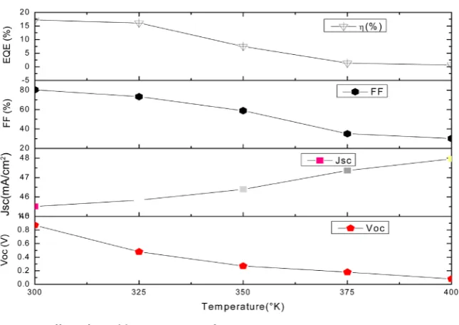
DOI: 10.4236/mnsms.2017.73003 40 Modeling and Numerical Simulation of Material Science 3.3.1. Effect of Variable Temperature of CdS
Figure 6 presents a simulated various temperature of solar cell with CdS buffer layer and shows the main photovoltaic parameters Voc, Jsc, FF and η. In this simulation, the temperature varies from 300 K to 400 K. As the temperature is increased, the Jsc is increased from 45.52 mA∙cm−2 to 47.16 mA∙cm−2 therefore
an increase of 4%∙Voc drops from 0.68 to 0.08 Volt therefore a decrease of 88%. As a result, the conversion efficiency η drops from 24.94% to 1.02% therefore a decrease of 96%.
3.3.2. Effect of Variable Temperature of ZnS
Figure 7 shows from 300 K to 400 K of varied temperature the main photovol-taic parameters Voc, Jsc, FF and η. In this simulation as the temperature is in-creased, the Jsc is increased from 45.55 mA∙cm−2 to 47.96 mA∙cm−2 therefore a
decrease of 6%. Voc dropped from 0.87 Volt to 0.08 Volt therefore a decrease of 90% and from 300 K to 400 K. FF declined from 80.33% to 30.15% therefore a decrease of 30% and the efficiency drops from 17.19% to 0.64% therefore a de-crease of 96%.
3.3.3. Effect of Variable Temperature of ZnSe
Figure 8 shows the performance parameters of the CIGS cell based on different values of temperature. Voc drops from 0.71 to 0.1 Volt therefore a decrease of 86%. Jsc increase from 45.78 to 47.9 mA∙cm−2 therefore an increase of 5%. From
300 to 350 K, FF increased 26.96 to 57.97 therefore a increase of 56% and from 350 K to 400 K. FF decreased from 57.97% to 33.13% therefore a decrease of 20% and conversion efficiency drops from 18.8 to 4.16% therefore a decrease of 78%.
DOI: 10.4236/mnsms.2017.73003 41 Modeling and Numerical Simulation of Material Science Figure 7. Effect of variable temperature of ZnS.
Figure 8. Effect of variable temperature of ZnSe.
3.3.4. Effect of Variable Temperature of In2S2
Figure 9 shows from 300 K to 400 K of varied temperature the main photovol-taic parameters Voc, Jsc, FF and η. In this simulation as the temperature is in-creased, the Jsc is increased from 45.58 mA∙cm−2 to 52.19 mA∙cm−2 therefore a
decrease of 14%. Voc drops from 0.68 Volt to 0.16 Volt therefore a decrease of 76% and from 300 to 400 K, FF declined from 79.47% to 30.65% therefore a crease of 30.65% and the efficiency drops from 16.1% to 1.24% therefore a de-crease of 92%.
DOI: 10.4236/mnsms.2017.73003 42 Modeling and Numerical Simulation of Material Science Figure 9. Effect of variable temperature of In2S2.
that when the temperature increases these electrons become unstable and re-combine with the holes before the carriers could reach the depletion region and collected [15]. The efficiency of the cells of PV parameter at higher temperature can be explained by other parameter like hole and the electron mobility carrier concentrations and band gaps of material would be affected high temperature [16].
3.4. Effect of Dual Buffer Layer
In order to improve the efficiency we simulated double buffer layer ZnS/CdS. Figure10 shows energy band of ZnS/CdS.
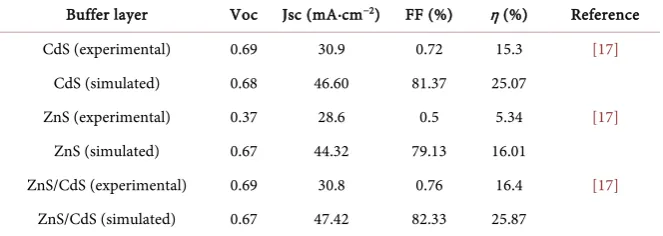
Table 3 shows that the main photovoltaic parameters are better with ZnS/CdS double layer than the CIGS solar cell with only ZnS layer and the same as that of the CIGS solar cell with conventional CdS layer and shows that efficiency in-creases from 25.07% to 25.87% so an increase of 3%.
We obtained a better efficiency that with an only ZnS layer because of inser-tion of CdS layer who have a superior juncinser-tion quality [16].
DOI: 10.4236/mnsms.2017.73003 43 Modeling and Numerical Simulation of Material Science Figure 10. Energy band of ZnS/CdS.
Figure 11. Spectral response for CIGS cell with a dual buffer layer ZnS/CdS.
4. Conclusion
The CdS buffer layer is replaced with fours materials. We first simulated a single buffer layer (CdS, ZnS, …) and determined the optimized CIGS solar cell and secondly we simulated a double buffer layer ZnS/CdS and the simulation proves that we have a good efficiency than a single buffer layer CdS or ZnS. The impact of changing material in the buffer layer of cell structure is evaluated and the op-timized efficiency is also determined using simulation tools. Simulation result shows that these materials can be used as buffer layer instead of toxic CdS in CIGS so-lar cell. Numerical simulation performed in this paper could contribute to fabri-cating a CIGS free solar cell. The results of simulations with the Solar Cells Capa-citance SCAPS reveal that CIGS solar cells with alternative buffer layers can be
300 400 500 600 700 800 900
40 50 60 70 80 90 100
Q
E
(%)
Wavelength(nm)
CdS ZnS/CdS ZnS
DOI: 10.4236/mnsms.2017.73003 44 Modeling and Numerical Simulation of Material Science Table 3. PV parameters of simulated and experimental double buffer layer ZnSe/CdS.
Buffer layer Voc Jsc (mA∙cm−2) FF (%) η (%) Reference
CdS (experimental) 0.69 30.9 0.72 15.3 [17]
CdS (simulated) 0.68 46.60 81.37 25.07
ZnS (experimental) 0.37 28.6 0.5 5.34 [17]
ZnS (simulated) 0.67 44.32 79.13 16.01
ZnS/CdS (experimental) 0.69 30.8 0.76 16.4 [17]
ZnS/CdS (simulated) 0.67 47.42 82.33 25.87
achieved. We concluded that ZnSe and ZnS can be used as alternative material to CdS, as it has serious environmental problems.
Acknowledgements
The authors are grateful to Prof Marc Burgelman and his colleagues at the Uni-versity of Gent for providing the SCAPS-1D software reported in this document.
References
[1] Résolution sur la conférence de Paris sur le climat (COP 21). [Paris Climate Change Agreement (COP 21).]
http://www.jugendparlament.lu/files/2015/07/Résolution_COP21.pdf
[2] http://www.PV-magazine.com
[3] Jamil, S. N-Abdulla, N. and Mohamned, K. (2012) Design and Fabrication Hetero-junction Solar Cell of Si-ZnO Thin Film. Proceeding of the International Confe-rence Nanomaterial Applications and Proprieties, 1, N4.
[4] Yamada, A., Chaisitsak, S., Ohtake, Y., and Konagai, M. (1998) High Efficiency Cu (In, Ga) Se2 Thin-Film Solar Cells with Novel Znnxsey Buffer Layer. Proceeding of
the 2nd World Conference of Photovoltaic Energy Conversion, 1, 1177-1180. [5] Enaoui, A., Eisele, W., Lex-Steiner, M.C., Riedl, W. And Karg, F. (2000) Cd-Free Cu
(Ga, In) (SSe) 2 Thin Film Solar Cells and Mini-Modules. 16th European
Photovol-taic Solar Energy Conference, Glasgow, 1-5 May 2000, 682-685.
[6] Pudov, A.O. (2005) Impact of Secondary Barriers on CuIn1−xGaxSe2 Solar-Celloperation
PhD Dissertation, Colorado State University Fort Collins, Colorado.
[7] Kessler, J., Ruckl, M., Harriskos, D. and Ruthle Schow, U. (2013) Interface Engi-neering between CuInSe2 and ZnO. Processing of the 23rd IEEE Photovoltaic Spe-cialist Conference, Louisville,16-21 June 2013, 447-452.
[8] Burgelman, M., Nollet, P. and Degrave, S. (2000) Modelling Polycrystalline Semi-conductor Solar Cells. Thin Solid Films, 361-362, 527-53.
https://doi.org/10.1016/S0040-6090(99)00825-1
[9] Malmstrom, J., Wennerberg, J., Khoshsirat, N., Amziah, N., Yunus, M., Hamidon, N.M. and Shafie, S. (2015) Analysis of Absorber Layer Properties Effect on CIGS Solar Cell Performance Using SCAPS. Optik, 125, 681-686.
DOI: 10.4236/mnsms.2017.73003 45 Modeling and Numerical Simulation of Material Science [11] Spiering, S., Eicke, A., Hariskos, D., Powalla, M., Naghavi, N. and Lincot, D. (2004) Large-Area Cd-Free CIGS Solar Modules with In₂S₃ Buffer Layer Deposited by ALCVD.
Thin Solid Films, 451-452, 562-566. https://doi.org/10.1016/j.tsf.2003.10.090
[12] Varshni, Y. (1967) Temperature Dependence of the Energy Gap in Semi-Conductor.
Physica, 34, 149-154. https://doi.org/10.1016/0031-8914(67)90062-6
[13] Ennaoui, A., Eisele, W., Lux-Steiner, M., Niesen, T.P. and Karg, F. (2003) Highly Efficient Cu(Ga,In)(S,Se)₂ Thin Film Solar Cells with Zinc Compound Buffer Lay-ers. Thin Solid Films, 431-432, 335-339.
https://doi.org/10.1016/S0040-6090(03)00155-X
[14] Brian, S. (2010) The Effect of Temperature on the Optimization of Photovoltaic Cells Using Silvaco ATLAS. Dissertation for Master. Electrical Engineering Naval Postgraduate School, Monterey.
[15] Chelvanathan, P., Hossain, M.I. and Amin, N. (2010) Performance Analysis of Copper-Indium-Gallium-Diselenide (CIGS) Solar Cells with Various Buffer Layers by SCAPS. Current Applied Physics, 10, S387-S391.
https://doi.org/10.1016/j.cap.2010.02.018
[16] Nakada, T. and Mizutani, M. (2002) 18% Efficiency Cd-Free Cu(In,Ga)Se2 Thin-Film
Solar Cells Fabricated Using Chemical Bath Deposition (CBD)-ZnS Buffer Layers. Ja-pan Society of Applied Physics, 41, 165. https://doi.org/10.1143/JJAP.41.L165
[17] Islam, M.M, Ishizuka, S., Yamada, A., Sakurai, K., Niki, S., Sakurai, T. and Akimoto, K. (2009) CIGS Solar Cell with MBE-Grown ZnS Buffer Layer. Solar Energy Mate-rials & Solar Cells, 93, 970-972. https://doi.org/10.1016/j.solmat.2008.11.047
[18] Hyeop Shin, D., Larina, L., Hoon Yoon, K. and Ahn, B.T. (2010) Fabrication of Cu(In,Ga)Se2 Solar Cell with ZnS/CdS Double Layer as an Alternative Buffer.