·-,, .
2019 south ritchcy street· santa ana. california 92705 · (714) 558-8211
CAL DATA 135
EMULATE BOARD,
( P /N C 81 0 8 0 21
o')
TECHNICAL MANUAL
C21518007-X2
Document C21518007 Revision X2
March 1975
cal Data, MACROBUS, QUADBOARD and HEXBOARD are trademarks of California Data Processors.
The information herein is the property of California Data
Processors. Transm~ttal, receipt or possession of :the
in-formation does not express, license or imply any rights to
use, sell or manufa~ture from this information and no
re-production or public~tion of it, in whole or in part shall
be made without written a~thorization from an officer of
the above firm.
REVISIONS
Revision Date Approval DescriEtion
X2 3-75
p
Revised and RedrawnThe revision history of each page in this document is indicated below: Revision
Page X2 I
i
v
ii v
1-1 v
1-2 ../
1-3 ../
2-1 v
2-2
v
2-3
v
2-4 v
2-5 I /
3-i
v
3-2
v
4-1
v
4-2
v
5-1 v
5-2
v
A-1 v
A-2 V"
A-3
v
A-4
v
A-5
v
A-6
v
A-7
v
A-8 v
B-1 v
B-2 v-··
B-3
v
SECTION 1: INTRODUCTION 1.1 SCOPE . . . • • 1.2 DOCUMENTATION . . • .
1.2.1 Publications . 1. 2.2
1. 2.3
Engineering Drawi_ngs .
Abbreviations and Conventions • . SECTION 2: FUNCTIONAL DESCRIPTION
2.1 2.2 2.3 2.4
GENERAL. . . . • • • • • • • • . EMULATE INSTRUCTION ADDRESS. EMULATE EXECUTE TABLE.
SPECIFICATIONS
SECTION 3: PHYSICAL DESCRIPTION 3.1
3.2
GENERAL . . CONNECTORS SECTION 4: INTERFACE 4.1
4.2 4.3
GENERAL. . SIGNALS • . CIRCUITS .
4.3.1 Line Driver • • 4.3.2 Line Receiver.
4.3.3 MACROBUS Loading • . SECTION 5: MAINTENANCE
5.1 5.2 5.3
GENERAL. . • • • •
PREVENTIVE MAINTENANCE • COEUIBCTIVE MAINTENANCE . .
APPENDICES
APPENDIX A: CONNECTOR PIN ASSIGNMENTS APPENDIX B: INSTRUCTION TIMING
CONTENTS
1-1 1-1 1-1 1-1 1-1 2-1 2-1 2-4 2-5 3-1 3-1 4-1 4-1 4-1 4-1 4-2 4-2 5-1 5-1 5-2Table 1-1 2-1 2-2 A-:1 A-2 A-3 A-4 A-5 A-6 A-7 A-8 B-1 B-2 B-3 B-4 Figure 1-1 2-1 2-2 3-1 i i
TABLES
Title ---Abbreviations.Emulation Sequences. . . • . . Cal Data 135 Emulate Board Specifications. Connector A Pin Assignments, MACROBUS. Connector B Pin Assignments, MACROBUS.
Connector C Pin Assignments. . . . . . Connector D Pin Assignments. . . • . .
Connector E Pin Assignments . . Connector F Pin Assignments . . Connector Jl Pin Assignments . Connector J2 Pin Assignments .
Single-Operand Instruction Timing (Microseconds) MOV(B) Instruction Timing (Microseconds) • . . .
Typical Double-Operand Instruction Timing (Microseconds): BIS(B), BIC (B), ADD, SUB . . . .
Control, Branch and Miscellaneous Instruction Timing . . . .
ILLUSTRATIONS
Title
Relationship of Publications to Cal Data 1 System Elements • . Cal Data 1 Computer System Organization. . . • . . • . . . . . Cal Data 135 Emulate Board Simplified Block Diagram. . . • Cal Data 135 Emulate Board
SECTION 1
INTRODUCTION
1.1
SCOPE
This manual provides the information needed to understand and maintain the Cal Data 135 Emulate Board (part number C81080210) when used with the drawing package provided. The information in this manual is for the use of a skilled technician familiar with standard test equipment, solid-state logic theory, common maintenance practices and standard troubleshooting techniques. A basic knowledge of design principles and circuits used in small computers is assumed, hence no tutuorial material of this kind is included.
As a stand-alone publication, this manual has a good functional and physical description of the Emulate Board, providing the information needed to understand the capabilities and features of the board. The maintenance coverage of this manual is connnensurate with the
pre-requisite skills and knowledge of the defined user, characteristics of the product and maintainability requirements established by Cal Data.
1.2
DOCUMENTATION
1. 2 .1
1. 2. 2
1. 2. 3
This manual describes the 135 Emulate Board of a Cal Data 1 Computer system that is equipped with a Cal Data 100 Engine (CPU) and a MACROBUS Channel Adapter (MCA) •
The following paragraphs define publications and conventions that support this manual.
Publications
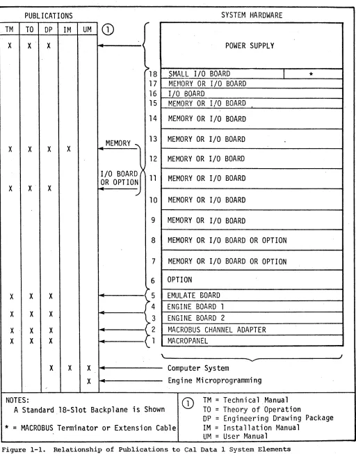
Figure 1-1 shows the relationship of system documentation to hardware elements. Controlled copies of publications, provided in accordance with the terms of the purchase contract, are kept current for the life of the product.
Engineering Drawings
For maintenance purposes, this manual is supported by a theory of operation and a drawing package that contains schematic diagrams, assembly drawings and other required engineering drawings. The drawing package is updated with the latest revision of each drawing.
Abbreviations and Conventions
Table 1-1 lists the abbreviations found in this manual. Conventions used in the text of this manual include:
a. Equipment panel nomenclature is reproduced in all upper-case characters.
PUBLICATIONS
SYSTEM HARDWARE
CD
/""TM
TO
DP
IM
UMx
x x
-
--
POWER SUPPLY
18
SMALL I/0 BOARD
I
*
17
MEMORY OR I/0 BOARD
16
I/0 BOARD
15
MEMORY OR I/0 BOARD
14
MEMORY OR I/0 BOARD
_MEMORY.:\
13
MEMORY OR 1/0 BOARD
-x
x
x
x
..
12
MEMORY OR I/0 BOARD
I/0 BOARD
><11
MEMORY OR I/0 BOARD
OR OPTION
x
x· x
-
...-10
MEMORY OR 1/0 BOARD
9
MEMORY OR I/0 BOARD
8
MEMORY OR 1/0 BOARD OR OPTION
7
MEMORY OR 1/0 BOARD OR OPTION
6
OPTION
>
x
x x
-
...
J5
EMULATE BOARD
4
ENGINE BOARD l
x
x
x
-·
--
3ENGINE BOARD 2
x
x x
--
--
2MACROBUS CHANNEL ADAPTER
x
x
x
-
...1
MACRO PANEL
..J
x x x
..
Computer System
x
--
--
Engine Microprogramming
/
NOTES:
CD
TM = Technical Manual
A Standard.18-Slot Backplane is Shown
TO = Theory of Operation
DP = Engineering Drawing Package
*
=
MACROBUS Terminator or Extension Cable
IM= Installation Manual
UM = User Manual
Figure 1-1. Relationship of Publications to Cal Data 1 System Elements
[image:6.612.42.554.45.702.2]C2158007-X2
b. The proper names of instructions, microconnnands and signals are capitalized.
c. ZERO and ONE are used to express binary logic "0" and "l" states, respectively.
d. Hexadecimal numbers are preceded by a dollar sign for easy identification.
e. A colon (:) is used to indicate a range of bi ts. For example
the range of Address bits Al2 to A04 is written Al2:A04. Table 1-1. Abbreviations
Abbreviation
-Cal Data CPU MCA ROM K EIA PSW I/O PC FR IR PS MS
cc
MB AB c~ Vdc psi kg/cm2 cfm lps0
c
µA mA ns -TTL
v
max min MeaningCalifornia Data Processors central processing unit {Engine) MACROBUS Channel Adapter
read-only memory
1,024 {addresses or memory locations) emulate instruction address
processor status word input/output
program counter file register
instruction register
- processor (macro) status register microstatus register
rnicroconunand location counter M bus
A-operand bus centimeter
volts, direct current pounds per square inch
kilograms per square centimeter cubic feet per minute
liters per second degrees, Celsius mi9roampere milliampere nanosecond
transistor-transistor logic volts
maximum minimum
[image:7.617.74.575.195.774.2]SECTION 2
FUNCTIONAL DESCRIPTION
2.1
GENERAL
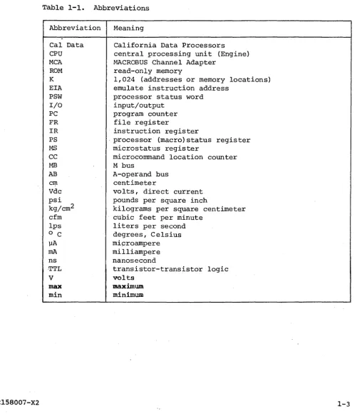
Emulate Boards are "language conentrators" that allow the Cal Data 100 Engine to emulate the functions performed by a variety of computers at
average speeds comparable to the machines being emulated. To the user,
the Cal Data 1 system with an Emulate Board (Figure 2-1) is transparent to all applicable software of the machine being emulated.
Because of differences in system architecture, some emulated instructions are executed faster and some slower in the Cal Data system with the
Emulate Board. For this reason, and due to the asynchronous operation
of the MACROBUS (whereby direct-memory-access devices can come on-line at any time), time-dependent program loops should be avoided to ensure complete program interchangability between the Cal Data 135 and the machine being emulated.
The Cal Data 100 Engine has all the elements of a very fast and versatile
CPU, but without an I/O structure. An I/O capability is provided by
an I/O channel adapter and associated I/O channel structure. For the
Cal Data 135 system, a MACROBUS Channel Adapter is used. These are
all the basic elements required for a successful emulation; however, such an emulation can be slow due to the distribution of data and control bits that must be analyzed in different emulated instructions. This
makes decoding and arithmetic comparisons difficult. The Emulate Board
works with the Engine to provide custom, high-speed instruction-decoding logic to perform the emulation at comparable average program speed.
2.2
EMULATE INSTRUCTION ADDRESS
To emulate instructions, the CPU executes appropriate firmware m~cro
command sequences from control memory. Depending on the instruction
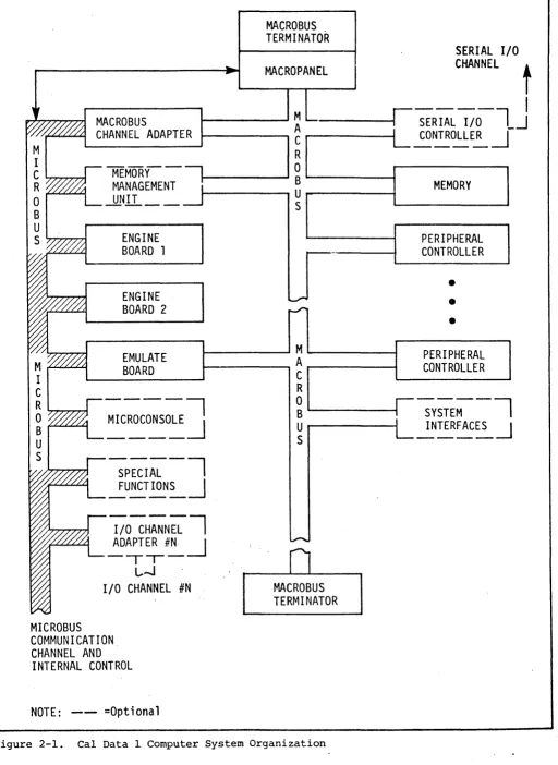
.being emulated, different sequences are executed in a specific order. To save time, Emulate Board logic (Figure 2-2) sufficiently decodes each instruction to determine the rnicrocommand sequence(s) to execute. Furthermore, the Emulate Board generates (by table lookup) the starting address within control memory of each required microcommand sequence. This address is called the emulate instruction address (EIA).
Three kinds of EIA are generated by the·Emulate Board, according to the sequence being processed:
a. Operand-sequence addresses from the emulate operand table
b. Execution-sequence addresses from the emulate execute table
c. CPU-interrupt vector addresses from the interrupt entry table
Table 2-1 shows the relationship between operand and execution sequences within the complete emulation for double-operand, single-operand and
MACRO BUS
TERMINATOR
MACRO PANEL
SERIAL 1/0
CHANNEL
t
MACROBUS
CHANNEL ADAPTER
.,.__ _ _
___,
~
- - - i l - ; R
IAL
l/o-l_J
J
CONTROLLER
_J
c
R
0MEMORY--MANAGEMENT
_iJ_NJl_ _ _
.,__ _ _ _ _ B
1---u
ENGINE
BOARD 1
ENGINE
BOARD 2
s
t---'-""
EMULATE
BOARD
.,..___ _ _ _ __... M _ _ _ _ _.
_ _ _ _ _ A _ _ _ _
- - t----,
MICROCONSOLE
_j
---,
SPECIAL
I
FUNCTIONS
_j
-l/o~HANNUI
ADAPTER #N-
_j
-,-,---L....J
I/O CHANNEL #N
MICROBUS
COMMUNICATION
CHANNEL AND
INTERNAL CONTROL
NOTE: ---- =Optional
c
R
0 s----~ u----~s
MACRO BUS
TERMINATOR
Figure 2-1. Cal Data 1 Computer System Organization
2-2
-MEMORY
PERIPHERAL
CONTROLLER
•
•
•
PERIPHERAL
CONTROLLER
---,
SYSTEM
I
INTERFACES
_J
[image:10.613.38.550.43.745.2]
() IV j...J l1l 00 0 0 ...]
I . :x: IV IV I :w t"rj
...
lQ i= Ii ('[) IV I IV () w j...J 0 llJ rt Ill j...J w l1l trjs
s:: j...J Ill rt CD tII 0 llJ Ii 0... Ul...
~
j...J...
Hi...
CD 0... to ~ ... 0 () ;ir.;-' 0...
llJ lQ Ii llJs
M Ic
R 0 Bu
s
IRl 5: IROO
INTERRUPT
EIA07: EIAOO
ENTRY
IRl 1:
IR09 IR VARIABLE
I R05: SELECTOR
IR03- - - '
TABLE (ROM)
EMULATE
EIAO?:
OPERAND
EIAOO
TABLE (ROM)
EMULATE
EIA15:
EXECUTE
EIAOO
TABLE (ROM)
TIMING
EMULATE
_I_R_l 5_:_I_RO_O _ _ _
... SCHEDULER
AND DECODER
IRS, IR?, IR2, IRl
EIA15:EIA12
Note:
~
= inputs to A-operand bus
via IR/PS/MS selector.
---IR/PS/MS
MULTIPLEXER
._~(INPUTS=~)
CPU
---__...MICROSTATUS
IR8,IR7, LOGIC AND
IR2, IRl
REGISTER
(MS)
CONTROL
LOGIC AND
CLOCKS
EXTERNAL
TIMING AND
CONTROL
. STATUS
MASK
.___ _ _
_... .. MSl 5 :MSl 3
PS03:PSOO
MS KO?: MS KOO
PS03:PSOO
PS03:PSOO
/t----+--M_B0_3_: _MB_O_O _ _ _ _ _ _ _ _ _ _ _ _
___;M....;.;;;B'--"-0....;;;...3..;;...;..: M:B....;;;...0-0=-.J,
.,.!>IPS VARIABLE
D03:000
MULTIPLEXER
PROCESSOR PS07:
MB07:MB04
·A--+---+-__;;_..;;..;_;~~ps
VARIABLE
- - - MACROBUS
MULTIPLEXER
STATUS
PSOO
REGISTER
(PS)
BUS
REQUESTS MACROBUS
PRIORITY
INTERRUPT
PSO?:PSOO
CONTROL
BUS GRANTS
015:000
007:000
[image:11.794.72.745.59.579.2]control instructions. CPU-interrupt vector addresses are enabled when needed by the interrupt priority l_ogic.
One or two operand sequences are required for each single- or
double-operand prograrmned instruction, r_espectively. Each operand sequence
fetches one operand from the appropriate location.
An execution sequence is required for the emulation of any instruction,
with or without operands. The execution sequence performs the function
specified by the emulated instruction. Although different instructions
often call for execution of the same operand sequences, each instruction
generally has a separate execution sequence. Firmware associated with
the execution sequence indicates the end of a complete emulation and enables the beginning of the next programmed instruction, if any.
An interrupt vector address is generated for each recognized interrupt.
Table 2-1. Emulation Sequences
Double-Operand Single-Operand Control
Step Instruction Instruction Instruction
1 Operand sequence Operand sequence Execution sequence
2 Operand sequence Execution sequence
--3 Execution sequence
--
--2.3
EMULATE EXECUTE TABLE
2-4
. ·.·~:--:·
The emulate execute table is an ROM addressed by selected control bits
of the instruction being emulated. For each possible combination of
bits selected by the variable selector and the decoder, and applied_ to the table, a 16-bit control word is output.
Eight bits of the output control word comprise the execution-sequence EIA
sent to the CPU microcoinmand location counter (CC). Four bits are used
for special control functions within the emulation logic.
The most-significant four .bits output from the emulate execute table control the modification of bits 03:00 of the processor status word (PSW).
This modification is under firmware control. These PSW bits are the status
flags required by the program (03 = negative, 02 = zero, 01 = overflow and 00 =carry). The emulate execute table provides rapid and specific updating of these bits in the single cycle following the execution of the instruction (i.e., just after the fetch for the next instruction is
issued). The updated PSW can be read from the Emulate Board at either
the macrolevel via the MACROBUS, or the microlevel via the A-operand bus
(AB; part of the Microbus). The instruction register (IR) or the micro_;.
status register (MS) can also be read via AB by execution of an appropriate
microcommand. The information placed on AB is determined by the emulate
IR/PS/MS multiplexer, which is controlled by the address generated in the A-operand field of the mi.crocommand.
2.4
SPECIFICATIONS
C2158007-X2
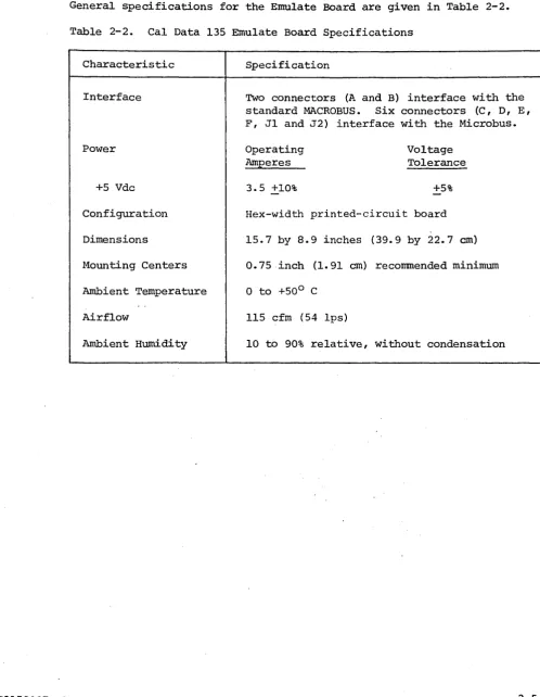
General specifications for the Emulate Board are given in Table 2-2. Table 2-2. Cal Data 135 Emulate Board Specifications
Characteristic Interface
Power +5 Vdc Configuration Dimensions
Mounting Centers Ambient Temperature Airflow
Ambient Humidity
Specification
Two connectors (A and B) interface with the standard MACROBUS. Six connectors (C, D, E, F, Jl and J2) interface with the Microbus. Operating
Amperes 3.5 +10%
Voltage Tolerance
+5% Hex-width printed-circuit board 15.7 by 8.9 inches (39.9 by 22.7 cm)
0.75.inch (1.91 cm) recommended minimum
o
to +50°c
115 cfm ( 54 lps)10 to 90% relative, without condensation
2-5
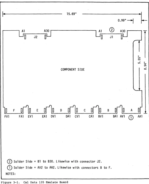
[image:13.615.65.564.110.753.2]SECTION 3
PHYSICAL DESCRIPTION
3.1
GENERAL
The Emulate Board {Figure 3-1) is a hex-width board 15.7 by 8.9 inches {39.9 by 22.7 cm) that normally plugs into slot 5 of the Cal Data com-puter chassis.* The right-hand edge of the board has a 1.0 by 5.5 inch
(2.5 by 14.0 cm) cutout as clearance for the side-mounted cooling fans in the chassis.
There are no controls or adjustable elements on the 135 Emulate Board.
3.2
CONNECTORS
C2158007-X2
There are six printed-circuit connectors (A to F) on the bottom edge of the board, and two (Jl and J2) on the top edge. Connectors A and B interface with the MACROBUS. Connectors C to F, and Jl and J2 interface with the main computer Microbus. Connectors A to F are standard back-plane connectors. Connectors Jl and J2 plug into two small
processor-interconnection boards.
*Because of the universal connections in the CPU area of the chassis, the Emulate Board can operate in any slot from 1 to 6.
15.69"
l-0.99" __,
Al
A30
Al
®
A30
D
J2
a
D
Jl
a
COMPONENT SIDE
FVl
FAl
EVl
EAl
DVl
DAl
CVl
CAl
BVl
BA 1 AVl
CD
Ml
(D
Solder Side= Bl to 830. Likewise with connector J2.
CD
Solder Side = AV2 to AA2. Likewise with connectors B to F.
NOTES:
Figure 3-1. Cal Data 135 Emulate Board
[image:16.618.32.551.79.720.2]SECTION 4
INTERFACE
4.1
GENERAL
The Emulate Board interfaces with the other computer boards via the chassis backplane, which includes the MACROBUS, and via two small interconnection boards spanning the tops of the computer boards. The interface with the MACROBUS (connectors A and B) conforms to the standard interfacing rules for I/O compatibility, described in the MACROBUS Channel Adapter Technical Manual, C21518013.
4.2
SIGNALS
Backplane connectors are labeled A to Fe A and B carry the MACROBUS, and C to F interface with the main computer Microbus. Connectors on the small processor-interconnection board are labeled Jl and J2. Pin assignments for all interface connectors are listed in Appendix A.
4.3
CIRCUITS
Because the Emulate Board is attached to the MACROBUS along with peripheral devices and memory, the MACROBUS loading.introduced by the board is an important system consideration for configurations with a large amount of memory or numerous peripheral devices. The Emulate Board minimizes the loading of receivers and the leakage current of drivers in the high state (these being the critical bus-loading para-meters). This is accomplished in two ways:
a. The driver leakage load is limited to that of one gate instead of two (as is conunon in some logic designs).
b. A Cal Data proprietary bus receiver circuit improves speed and reduces drive requirements.
4.3.1
Line Driver
C2158007-X2
The line driver is a TTL buffer. The critical MACROBUS specifications for the device are:
Output low voltage at 50 mA
sink (V 0L)
Output high leakage current at 2.5
v (IoH>
+0.5
v
max +60 µA max4.3.2
4.3.3
4-2
Line Receiver
The Emulate Board uses a Cal Data line receiver. The critical MACROBUS specifications for this device are:
Input high threshold (VIH) Input low threshold (VIL) Input current at +2.5 V (IIH) Input current at O.O V (IIL)
MACROBUS Loading
+2.5Vmin +1.4
v
max +60 µA max +25 µA maxThe limiting MACROBUS loading occurs on the bidirectional data lines that have one receiver and one driver for each I/O module. Worst-case MACROBUS load specifications are:
+2.5 V min +1.4 V max
+120 µA max at +2.5 V +25 µA max at 0.0 V
5.1
GENERAL
SECTION
"5
MAINTENANCE
This section describes preventive and corrective maintenance procedures that apply to the Cal Data 135 Emulate Board. In general, corrective maintenance is limited to the isolation of a fault to the Emulate Board
followed by replacement of the board. Troubleshooting can then be used to verify that the suspected module is malfunctioning and to help
diagnose the specific problem. Repair should be conducted at the factory or by an authorized representative.
5.2
PREVENTIVE MAINTENANCE
The Emulate Board is a reliable solid-state device designed to perform continuously for many years. Preventive maintenance consists of per-forming the following tasks every six months:
a. Inspect the board for damaged wires, components or other obvious defects.
b. Using a low-pressure source of air (75 psi one foot from the board or 5 kg/cm2 30 cm from the board), blow off accumulated dust and foreign matter.
Another aspect of preventive maintenance is proper handling of the board. The following points should be observed:
a. Always be sure that system power is OFF before installing or re-moving any board.
b. Install each board with the component side toward the front of the chassis. Check each board for proper orientation before attempting to install it. Because the connectors are keyed, excessive force applied to a reversed board can result in con-nector damage. Make sure that the board is completely and evenly seated.
c. Insert and remove each board slowly and carefully so that i t does not make contact with adjacent boards.
d. Never use components as finger grips; use the grip areas at the corners of the board.
e. To prevent oxides from forming on the gold plating, do not touch connectors.
5.3
CORRECTIVE MAINTENANCE
5-2
Repair or adjustment of the Emulate Board in the field is not recommended. If a malfunction is detected, replace the board with a spare known to be operating properly and return the malfunctioning board for repair to California Data Processors or an authorized representative.
n N ... U1 0) 0 0 -..J I :><: N )ii I ...
·Name Signal Pin Pin Signal Name
Initialize ·*BUS INIT-L Al A2 +SV +5 Vdc
Interrupt *BUS INTR-L Bl B2 GND Ground
Data 00 BUS DOO-L Cl C2 GND Ground
Data 02 BUS D02-L Dl D2 BUS DOl-L Data 01
Data 04 BUS D04-L El E2 BUS D03-L Data 03
Data 06 BUS D06-L Fl F2 BUS DOS-L Data 05
Data 08 BUS D08-L Gl H2 BUS D07-L Data 07
Data 10 BUS DlO-L Jl J2 BUS D09-L Data 09
Data 12 BUS Dl2-L Kl K2 BUS Dll-L Data 11
Data 14 BUS Dl4-L Ll L2 BUS Dl3-L Data 13
Parity Bit Low *BUS PA-L Ml M2 BUS DlS-L Data 15
Ground GND Nl N2 *BUS PB-L Parity Bit High.
Ground GND Pl P2 *BUS BBSY-L Bus Busy
Ground GND Rl R2 *BUS SACK-L Selection Acknowledge~ent
Ground GND Sl S2 *BUS NPR-L Nonprocessor Request
Ground GND Tl T2 BUS BR7-L Bus Request 7
Non processor Grant *BUS NPG-H Ul U2 BUS BR6-L Bus Request 6
Bus Grant 7 *BUS BG7-H Vl V2 GND Ground
* These signals are assigned on the backplane but are not used on this assembly.
n 0 ::s ::s It> 0 rt 0 11 )ii "'d
,_..
::s )ii rn rn,_..
lO§
It> ::s rt rn ...0
0
z
z
fTI
0
-f
0
::0
-0
-z
l>
(/) J>
~
""C
C>
-0
z .,,
s:
z
.,, c
z
() N
"-'
U1
CX>
0 0 ...J
I
><
~
Name Signal Pin Pin Signal Name
Bus Grant 6 *BUS BG6-H Al A2 +sv +5 Vdc
Bus Grant 5 *BUS BGS-H Bl B2 GND Ground
Bus Request 5 BUS BRS-L Cl C2 GND Ground
Ground GND Dl 02 BUS BR4-L Bus Request
Ground GND El E2 *BUS BG4-H Bus Grant 4
AC Low *BUS ACLO-L Fl F2 *BUS DCLO-L DC Low
Address 01 BUS AOl-L Hl H2 *BUS AOO-L Address 00
Address 03 BUS A03-L Jl J2 BUS A02-L Address 02
Address OS BUS AOS-L Kl K2 BUS A04-L Address 04
Address 07 BUS A07-L Ll L2 BUS A06-L Address 06
. Address 09 BUS A09-L Ml M2 BUS A08-L Address 08
Address 11 BUS All-L Nl N2 BUS AlO-L Address 10
Address 13 BUS A13-L Pl P2 BUS Al2-L Address 12
Address 15 BUS Al5-L Rl R2 BUS Al4-L Address 14
Address 17 BUS Al7-L Sl S2 BUS Al6-'L Address 16
Ground GND Tl T2 BUS Cl-L Control 1
Slave Synchronization BUS SSYN-L Ul U2 *BUS CO-L Control 0
Master Synchronization BUS MSYN-L Vl V2 GND Ground
*
These signals are assigned on the backplane but are not used on ~his assembly. 4()
0
::s ::s
CD
0
rt
0
t1
tJj
~
...
::s
):I
en en
,....
l.Q ::s
~
::s
rt
en
. ,5
(') .
N·
t-'
ln .
(l) 0 0 -...J I :x: t\J !J:il I w Name M Bus 00 ·M Bus 01 M Bus 02 M Bus 03 M Bus 05 M Bus 07 M Bus 09 M Bus 11
M Bus 13 M Bus 15 A Bus 01 A Bus 03 A Bus 05 A Bus 07 A Bus 09 Ground A Bus 13 A Bus 15
Signal Pin
MBOOO-L Al MBOOl-L B2 MB002-L Cl MB003-L Dl MBOOS-L El MB007-L Fl MB009-L Hl MBOll-L Jl MB013-L Kl MB015-L Ll ABOOl-H Ml AB003-H Nl AB005-H Pl AB007-H Rl AB009-H Sl
GND Tl
ABOl.3-H Ul AB015-H Vl
Pin Signal
A2 +5V
B2 -lSV
C2 GND
02 MB004-L E2 MB006-L F2 MB008-L H2 MBOlO-L J2 MB012-L
K2 MB014-L L2 ABOOO-H M2 AB002-H N2 AB004-H P2 AB006-H
R2 ABOOB-H
S2 ABOlO-H T2 ABOll-H U2 AB012-H V2 AB014-H
Name +5 Vdc -15 Vdc Ground M Bus 04 M Bus 06 M Bus 08 M Bus 10 M Bus 12 M Bus 14 A Bus 00 A Bus 02 A Bus 04 A Bus 06 A Bus 08 A Bus 10 A Bus 11 A Bus 12 A Bus 14
8
g.
t-' Ct>:r
w.
(') 05
Ct> Cl rt 0 ~ (') t1j...
:;3 ~ (/)i"
:;3rt
()
r-.J
... l11
co
0 0 ....J
I
x
-!\.)'
Name Signal Pin Pin Signal Name
Power Failure Interrupt PFINT-H Al A2 +5V +5 Vdc
Halt Interrupt HLINT-H Bl B2 *-15V -15 Vdc
Data Switch 16 * DS16-H Cl C2 GND Ground
Data Switch 17 * DSl 7-H Dl D2 * LTCL-L Line-Frequency Clock Virtual Address * VIRTAD-H El E2 * PBBSY-L Processor Bus Busy
Control Count 00 * CCOOO-L Fl F2 HALTP-L Panel Halt
Control Count 01 * CCOOl-L Hl H2 *MSR15-L Microstatus_ Register 15
Control Count 02 * CC002-L Jl J2 RESET-L Reset
Control Count 03 * CC003-L Kl K2 *BUS BG7-IN Bus Grant 7 In Control Count 04 * CC004-L Ll L2 BUS BG7-0UT Bus Grant 7 Out Control Count 05 * CC005-L Ml M2 *BUS BG6-IN Bus Grant 6 In Control Co9nt 06 * CC006-L Nl N2 BUS BG6-0UT Bus Grant 6 Out Control Count 07 * CC007"'."L Pl P2 *BUS BGS-IN Bus Grant 5 In Control- Count 08 * CC008-L Rl R2 BUS BGS-OUT Bus Grant 5 Out Control Count 09 * CC009-L Sl S2 *BUS BG4-IN Bus Grant 4 In
Ground GND Tl T2 BUS BG4-0UT Bus Grant 4 Out
Control Count 10 * CCOlO-L Ul U2 *BUS NPG-IN Nonprocessor Grant In Control Count 11 * CCOll-L Vl V2 *BUS NPG-OUT Nonprocessor Grant Out
)ii I
lJ1
. ··-··
Name Signal Pin Pin signal Name
Control Memory 00 CMOOO-H Al A2 +sv +5 Vdc
Control Memory 01
*
CMOOl-H Bl B2*
-15V -15 VdcControl Memory 02 * CM002-H Cl C2 GND Ground
Control Memory 03
*
CM003-H .Dl 02 * CM004-H Control Memory 04Control Memory 05
*
CMOOS-H .El E2 CM006-H Control Memory 06Control Memory 07
*
CM007-H Fl F2 * EMINH-L Emulate InhibitControl Memory 09
*
CM009-H Hl H2 * CM008-H Control Memory 08Control Memory 11
*
CMOll-H Jl J2*
CMOlO-H Control Memory 10Decode Address 00
*
DADOO-H Kl K2 * CM012-H Control Memory 12Control Memory 13
*
CM013-H Ll L2 * CM014-H Control Memory 14Control Memory 15 * CMOlS-H Ml M2 * DADOl-H Decode Address 01
Control Memo.~y 17
*
CMOl 7-H Nl N2 * CM016-H Control Memory 16Control Memory 19 * CM019-H Pl P2 * CM018-H Control Memory 18
Switch Register 0 * SRO-L Rl R2 * CM020-H Control Memory 20
Control Memory 21 * CM021-H Sl S2 * CM022-H Control Memory 22
Ground GND Tl T2 CM024-H Control Memory 24
Control Memory 23
*
CM023-H Ul U2 CM026-H Control Memory 26Control Memory 25 CM025-H Vl V2 CM027-H Control Memory 27
*
These signals are assigned on the backplane but are not used on this assembly.()
0
::s ::s
CD
(')
rt
0 11
t:rj tU I-'· ::s ):ii
en
en
...
"°
§
CD
::s rt
(") N 1--1 U1 CD 0 0 -..J
I, .. ::< •.
N
Name Signal Pin Pin Signal Name
Control Memory 28 CM028-H Al A2 +5v +5 Vdc
Control Memory 29 · * CM029-H Bl B2 *-15V -15 Vdc
Control Memory 31 * CM031-H Cl C2 GND Ground
Control Memory 31
*
CM030-H Dl 02 *CM032-H Control Memory 32 Control Memory 33 * CM033-H El E2 *CM034-H Control Memory 34 Control Memory 35 * CM035-H Fl F2 *DAD02-H Decode Address 02 Control Memory 37 * CM037-H Hl H2 *CM036-H Control Memory 36 Control Memory 39 * CM039-H Jl J2 *CM038-H Control Memory 38 Instruction Repeat IRPTE-L Kl K2 *CM040-H Control Memory 40 Control Memory 41 * CM041-H Ll L2 *CM042-H Control Memory 42 Control Memory 43 * CM043-H Ml M2 *CPEN-L Control Panel Enable Control Memory 45 * CM045-H .Nl N2 *CM044-H Control Memory 44 Control. Memory 47 * CM047-H Pl P2 *CM046-H Control Memory 46Decode Address 03 * DAD03-H Rl R2 *ACMSL-L Alterable Control Memory Select Reserved Sl S2 *AUXRM-L Auxiliary ROM Select
Ground GND Tl T2 IRINH-L Instruction Inhibit
Reserved Ul U2 IWAIT-L Instruction Wait
System Clock SYSCK-L Vl V2 GND Ground
n
"'
I-' 01
co
0 0
....J
I
:><:
N
Name Signal Pin Pin Signal Name
Skip
*
SKIPP-L lA lB EMAOO-H Emulate Address 00AR Write Enable ARWEN-L 2A 2B EMAOl-H Emulate Address 01
Stack Limit Write Enable
*
SLWEN-L 3A 3B EMA02-H Emulate Address 02 Slave Synchronization Error SSYER-H 4A 4B EMA03-H Emulate Address 03 Double Slave Synchronization DSYER-H SA SB EMA04-H Emulate Address 04Error
Load Special Function LDSPF-H 6A 6B EMAOS-H Emulate Address OS Fatal Interrupt
*
FINTP-L 7A 7B EMA06-H Emulate Address 06Special Function SPFNC-H 8A SB EMA07-H Emulate Address 07
Panel Halt HALTP-L 9A 9B Reserved
Reserved lOA lOB
*
PSSEL-L Program Status SelectCarry
*
CARRY-H llA llB ReservedReserved 12A 12B Reserved
Address Error ADERR~H 13A 13B Reserved
Program Status 03 PS003-L 14A 14B Reserved
Reserved lSA lSB
*
XD007-L Inhibit Destinat~on File 0 to 7 Reserved 16A 16B*
XD815-L Inhibit Destination File 8 to 15 Reserved 17A 17B*
XB815-L Inhibit B-Field File 8 to 15 Control Count Write Enable*
CCWEN-H 18A 18B*
XB007-L Inhibit B-Field File 0 to7
Static Condition
*
STATIC-L 19A 19B*
LITRL-L _,,Literal Master Synchronization MSYN-H 20A 20B*
PLUSl-L Plus 1Special Function 04 SPF04-L 21A 21B PSWEN-L Processor Status Write Enable B Bus Inhibit
*
BBINH-L 22A 22B IRWEN-L IR Write EnableB Bus 01
*
BBOOl-H 23A 23B*
BBOOO-H B Bus 00B Bus 03
*
BB003-H 24A 24B*
BB002-H B Bus 02B Bus 05
*
BBOOS-H 25A 25B*
BB004-H B Bus 04B Bus 07
*
BB007-H 26A 26B*
BB006-H B Bus 06B Bus 09
*
BB009-H 27A 27B*
BB008-H B Bus 08B Bus 11
*
BBOll-H 28A 28B*
BBOlO-H B Bus 10B Bus 13
*
BB013-H 29A 29B*
BB012-H B Bus 12B Bus 15
*
BB015-H 30A 30B*
BB014-H B Bus 14)II I
(X)
n N
...
U"I
(X)
0
0
....,
I .::<·-,
N
Name
Signal Pin Pin Signal NameLoad CC Register
*
LOADC-L lA lB ReservedBus Request
*
BREQ-H 2A 2B MINTP-L MicrointerruptBus Grant BGRNT-L 3A 3B
*
BYTDA-L Byte DataBus Grant Enable BGEN-H 4A 4B Reserved
Memory Management Inhibit MMINH-L SA SB
*
MARLD-H Management Address Load Data Inhibit*
DAINH-L 6A 6B*
CCCEN-H CC Count EnableSpecial Function 7
*
SPF07-L 7A 7B*
SPRlA-L Special Register lASpecial Function 5
*
SPFOS-L 8A BB*
SPR19-L Special Register 19 Special Function 6*
SPF06-L 9A 9B*
SPRlB-L Special Register lB Special Function Decode*
SPFNC-H lOA lOB*
MLTPY-L MultiplyInhibit B Field INHBF-L llA llB
*
ENSPF-H Enable Special FunctionEmulate EMLAT-H 12A 12B CR008-H Microcommand Register 08
Power Failure PFAIL-L 13A 13B Reserved
AU Carry In
*
AUCIN-L 14A 14B ReservedWrite WRITE-L lSA lSB FILE6-H File 6
IR Read IRERD-H 16A 16B
*
XA815-L Inhibit A-Field File 8 to 15 Interrupt INTR..,.ff 17A 17B*
XA007-L Inhibit A-Field File 0 to 7 Memory Managementco
*
MMCO-L 18A 18B*
RSTRA-L Restore AMemory Management Cl
*
MMCl-L 19A 19B YELLW-L Yellow Microcornmand Register 07 CR007-H 20A 20B BYTMD-L Byte ModeStack Limit Interrupt SLINT-H 21A 21B
*
MS006-H Microstatus Register 06 DR Write Enable*
DRWEN-L 22A 22B*
RRWEN-L RR Write EnableEmulate Instruction Address 01 EIAOOl-H 23A 23B EIAOOO-H Emulate Instruction Address 00 Emulat:. Instruction Address 03 EIA003-H 24A 24B EIA002-H Emulate Instruction Address 02 Emulate Instruction Address 05 EIAOOS-H 2SA 2SB EIA004-H Emulate Instruction Address 04
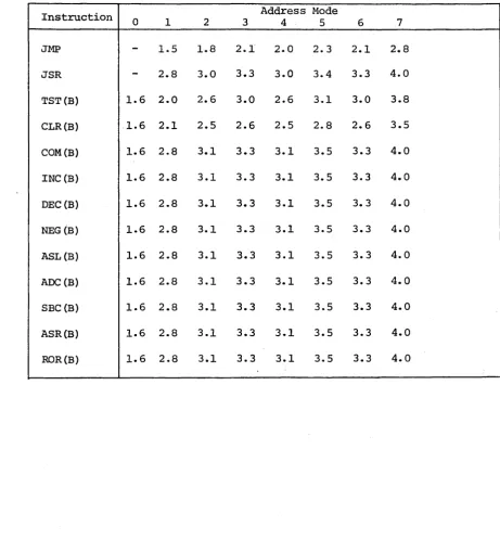
APPENDIX B
INSTRUCTION TIMING
The tables in this appendix give approximate instruction execution times for the Cal Data 135. The values given have a tolerance of
ten percent and are calculated assuming a 165-ns clock and one Cal Data 8KX16 memory module as the main storage element.
Table B-1. Single-Operand Instruction Timing (Microseconds) Instruction 0 1 2 3 Address Mode
4 5 6 7
JMP
-
1.5 1.8 2.1 2.0 2.3 2.1 2.8JSR
-
2.8 3.0 3.3 3.0 3.4 3.3 4.0TST(B) 1.6 2.0 2.6 3.0 2.6 3.1 3.0 3.8 CLR(B) 1.6 2.1 2.5 2.6 2.5 2.8 2.6 3.5 COM(B) 1.6 2.8 3.1 3.3 3.1 3.5 3.3 4.0 INC(B) 1.6 2.8 3.1 3.3 3.1 3.5 3.3 4.0 DEC (B) 1.6 2.8 3.1 3.3 3.1 3.5 3. 3 4.0 NEG(B} 1.6 2.8 3.1 3.3 3.1 3.5 3.3 4.0 ASL(B} 1.6 2.8 3.1 3.3 3.1 3.5 3.3 4.0 ADC(B) 1.6 2.8 3.1 3.3 3.1 3.5 3.3 4.0 SBC(B) 1.6 2.8 3.1 3.3 3.1 3.5 3.3 4.0 ASR(B) 1.6 2.8 3.1 3.3 3.1 3.5 3.3 4.0 ROR(B} 1.6 2.8 3.1 3.3 3.1 3.5 3.3 4.0
[image:29.615.110.571.241.750.2]Table B-2. MOV(B) Instruction Timing (Microseconds)
Destination Source Mode
Mode 0 1 2 3 4 5 6 7
0 2.0 2.6 2.6 3.3 2.6 3.3 3.3 4.1
1 2.5 3.1 3.1 3.8 3.1 3.8 3.8 4.6
2 2.8 3.6 3.6 4.3 3.6 4.3 4.3 5.1
3 3.0 3.8 3.8 4.5 3.8 4.5 4.5 5.6
4 2.8 3.6 3.6 4.3 3.6 4.3 4.3 5.1
5 3.1 4.0 4.0 4.6 4.0 4.6 4.6 5.4
6 3.0 3.8 3.8 4.5 3.8 4.5 4.5 5.3
7 3.6 4.5 4.5 5.1 4.5 5.1 5.1 5.9
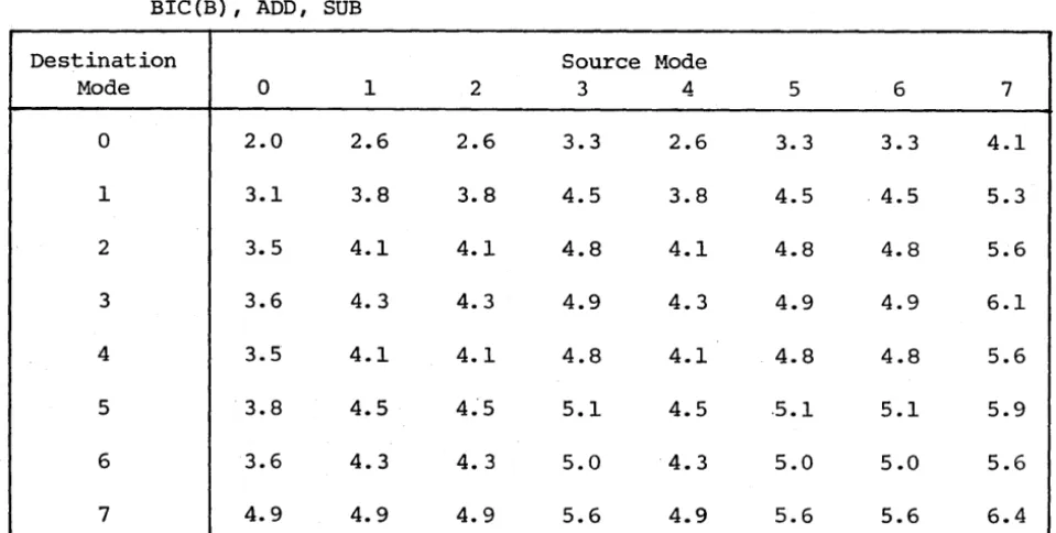
Table B-3. Typical Double-Operand Instruction Timing (Microseconds): BIS(B), BIC(B), ADD, SUB
Destination Source Mode
Mode 0 1 2 3 4 5 6 7
0 2.0 2.6 2.6 3.3 2.6 3.3 3.3 4.1
1 3.1 3.8 3.8 4.5 3.8 4.5 . 4.5 5.3
2 3.5 4.1 4.1 4.8 4.1 4.8 4.8 5.6
3 3.6 4.3 4.3 4.9 4.3 4.9 4.9 6.1
4 3.5 4.1 4.1 4.8 4.1 4.8 4.8 5.6
5 3.8 4.5 4.· 5 5.1 4.5 .5.1 5.1 5.9
6 3.6 4.3 4.3 5.0 4.3 5.0 5.0 5.6
7 4.9 4.9 4.9 5.6 4.9 5.6 5.6 6.4
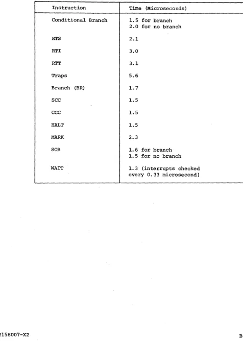
[image:30.624.50.530.410.652.2]Table B-4. Control, Branch and Miscellaneous Instruction Timing Instruction Time (Microseconds)
Conditional Branch 1. 5 for branch 2.0 for no branch
RTS 2.1
RTI 3.0
RTT 3.1
Traps 5.6
Branch (BR) 1. 7
sec 1.5
CCC 1.5
HALT 1.5
MARK 2.3
SOB 1.6 for branch
1.5 for no branch
WAIT 1. 3 (interrupts checked
every 0.33 microsecond)
[image:31.624.74.551.93.762.2]