© 2019, IRJET | Impact Factor value: 7.211 | ISO 9001:2008 Certified Journal | Page 1409
DADDA ALGORITHM BASED LOWPOWER HIGH SPEED MULTIPLIER
USING 4T XOR GATE
Neethu R S
1, Aneesh S P
2, Saju A
31
PG Scholar, Department of ECE, Musaliar College of Engineering and Technology, Kerala, India
2
Assistant Professor, Department of ECE, Musaliar College of Engineering and Technology, Kerala, India
3
Associate Professor, Department of ECE, Musaliar College of Engineering and Technology, Kerala, India
---***---Abstract -
This paper describes efficient method to design a4-bit multiplierhaving low power, area and high speed using the Dadda algorithm and the basic building block of multiplier’s used a 14T Full adder having low power dissipation. Full and half adder blocks have been designed using 4T XOR gate to reduce the power dissipation and Dadda algorithm to reduce the propagation delay. The model has been designed using DSCH 2 and Micro wind tool.
Key Words: 4T XOR gate, 14T full adder, Dadda
algorithm, 4x4 Multiplier
1. INTRODUCTION
The electronic world is growing day by day. So the demand for electronic components is increased. But the electronic component faces the power dissipation speed, the area is major problems. The ALU is taking more power in the electronic components. The major parts of ALU are adder and multipliers. Multipliers play an important part in digital signal processing and various other applications. The basic method of multiplication is added and shift algorithm. In parallel multipliers number of partial products to be added is the main parameter that determines the performance of the multipliers. The product is the result of multiplying the multiplicand to the multipliers. The multiplication operation is performed in two main steps. First is the partial product formation which consists of multiplying each bit of the multiplier with multiplicand. Each progressive fractional item has a general move of one-bit position to left side of the previous partial product. The second step is partial product accumulation where the partial product is combined to find the result. The essential requirement of multiplier include high-speed, low power consumption technique is the best method for these achievements. Wallace and Dadda multipliers are the column compression multipliers. Wallace, Array, and Dadda multipliers have been done and proved thatthe Dadda multiplier is better than the other multipliers. Dadda Multipliers have faster performance. So it used for the proposed technique and compared with the regular Dadda multipliers and Wallace tree and array multipliers.
1.1 Parallel Multipliers
Parallel multipliers are used for high-performance devices because it has high speed and low delay than the
serial multipliers. A parallel multiplier is two types of Array multipliers and Tree Multipliers.
A Array Multiplier
The Multiplier multiplied two numbers and it produced partial products and the adder circuit is used to add the partial products then it produced the final product. The array multiplier required N(n-1) adder circuits and N² AND gates. Array Multiplier has a simple circuitry so it is easy to implement.
Fig -1: Block diagram of Array Multiplier
B Wallace tree multiplier
[image:1.595.312.553.361.516.2]© 2019, IRJET | Impact Factor value: 7.211 | ISO 9001:2008 Certified Journal | Page 1410
with respect to the previous stage or intermediatematrix. For reducing heights adders are used. So the reduced intermediate matrix is given below which has the height of six. Notice that vacant or unused bits are placed first followed by the sum of the adder followed by the carry of the previous step. Here calculation starts from the LSB side. 7. Step 3: Addition of partial products. Then the matrix of height two is added by any known adder like carry select adder or parallel adder etc. The final sum which will be the result of the multiplication.
Fig -2: Block diagram of Wallace tree Multiplier
C Dadda tree algorithm
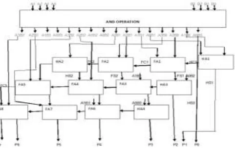
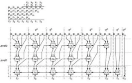
[image:2.595.46.278.220.365.2]Different algorithms have been proposed to decrease the propagation delay during the addition of the partial products generated by AND Gate. One of the most efficient algorithms is Dadda algorithm. The proposed 4*4 multiplier has a total of 16 partial products, so, the height of the tree is four as shown Fig. 3. Dadda Algorithm has been applied for the purpose to reduce the height of the tree from four to two. If we do not apply Dadda algorithm, then we must have to wait for the previous stage to simulate it, because, the next stage uses the carry of the previous stage which will increase the propagation delay [8]. For this simple technique, we have to use the ripple carry adder, it also consumes less power, but the delay is significantly high. To reduce the overall propagation delay of the multiplier Dadda algorithm has been applied. This is the best technique for reduction in the delay of the overall multiplier design because, at the start, it does not depend on the previous stage. Therefore, the first stage will be implemented without depending on any other stage. First, we have arranged our partial products to make a tree as shown in Fig. 4. These partial products are generated by the AND gate. The height of this tree is 4 as the proposed design is the 4-bit multiplier.
Stages of dadda algorithm
The objective is to reduce the height of the tree from four to two. Therefore, building blocks have been used in such a way to reduce the tree height from four to three after
the completion of first Dadda stage and then from three to two after the completion of the second Dadda Stage [11]. Furthermore, the two Dadda stages are used to reduce this tree. The first and second Dadda stages are shown inFig. 4 and Fig.5, respectively. Proposed System The major part of ALU is multiplier and adder circuit. These circuits take more area and provide high power dissipations. This paper included the design of low power adder circuits and used Dadda algorithm is the method to reduce the overall propagation delay, area and power dissipation of the multiplier. The major blocks of a multiplier are AND GATE, Full adder, and half adder. Area and power dissipation of these circuits will reduce the overall power dissipation, area. So this paper is given a new multiplier design with the reduced area, power, and delay.
2. PROPOSED MULTIPLIER
The major blocks of a multiplier are AND GATE, Full adder, and half adder. Area and power dissipation of these circuits will reduce the overall power dissipation, area. So this paper is given a new multiplier design with the reduced area, power, and delay.
Design of AND gate
[image:2.595.318.568.290.444.2]© 2019, IRJET | Impact Factor value: 7.211 | ISO 9001:2008 Certified Journal | Page 1411
Table -1: Comparison of power for AND gate usingdifferent logics
Type of
Logic No. of transi stors used
Power Consumption (microwatt)
Surface Area
(micrometer2 )
CMOS AND 6 7.382 97.7
Pass transistor Logic
2 0nW 21.9
Transmission
gate Logic 4 1.302 41.2
Logic Circuit 6 1.965 19.2
Design of Full adder
Full adder is the major element of a multiplier. The design of full adder is more concentrate and aware.
Table -2: Truth table of Full adder
A B C SUM CARRY
0 0 0 0 0
0 0 1 1 0
0 1 0 1 0
0 1 1 0 1
1 0 0 1 0
1 0 1 0 1
1 1 0 0 1
1 1 1 1 1
Construction
S=A XOR B XOR C
CARRY= AB+(C (A XOR B))
=AB+C (A’B+AB’)
=AB+A’BC+AB’C
=B (A+A’C) +AB’C
=BAC+AB’C
=C (A XNOR B)
=C (A XOR B)
The main part of full adder design is the XOR gate which generates basic addition operation in the adder circuits.
[image:3.595.35.566.392.732.2]A single XOR generates simple two bit addition. The XOR gate conventionally uses 8 MOSFETs for proper working, however, at present we have different XOR gate topologies [6] [7]. However, in this project have used to design a 4T XOR gate to get low power consumption. An XOR gate or Exclusive OR gate is a digital logic gate with two or more inputs and one output that performs an exclusive function. The true output results if one, and only one of the inputs to the gate is true (logic 1). If both inputs are false (logic 0) and both are true (logic 1), a false (logic 0) output results. A B Output 0 0 0 0 1 1 1 0 1 1 1 0 This 4T XOR gate is used to design a 14T full adder circuit [3] which provide less power dissipation than the static CMOS full adder, pass transistor logic, transmission logic.4T XOR gate used 14T adder consists of 14 transistors provide considerably less power in the range of microwatts and has higher speed. In the 14T full adder, we used 4T XOR gate and inverted 4T XOR gate. 8 MOSFETs used Conventional XOR gate for proper working, but present we have different topologies. Here we have used 4T XOR gate to reduce overall area and power dissipation. Using this XOR gate, reduction in the size of a full adder is achieved and overall leakage is also reduced.4T XoR to increase circuit density [4] [5].
Table -3: Truth table of EXOR gate
A B Output
0 0 0
0 1 1
1 0 1
1 1 0
Table -4: Comparison of Power for full adder Using Different Logics
Type of Logic No. of transisto rs used
Power Consumptio n
(microwatt)
Surface Area (micrometer2 )
Static CMOS
transistor 28 15.231 1061.4
Normal PTL {sum}
Normal PTL{Carry}
20
24
11.52 11.740
63.2 215.9
Transmission
gate logic 20 14.915 521.1
© 2019, IRJET | Impact Factor value: 7.211 | ISO 9001:2008 Certified Journal | Page 1412
Design of half adder [image:4.595.86.549.46.411.2]Expression:-SUM=AB+AB =A XOR B CARRY =AB Half adder circuit has two input and two output, Sum and Carry. The result of the SUM is EXOR function. So 4T XOR gate is used to design the Sum function and logic AND is used for Carry function.
Table -5: Truth table of half adder
A B Sum Carry
0 0 0 0
0 1 1 0
1 0 1 0
1 1 1 1
Table -6: Simulation result ofhalf adder
Type of
Logic No. transistor of
used
Power consumption( Microwatt)
Surface Area (Micrometer 2)
4T
transistor 10 2.045 72.7
Design of proposed multiplier
The multiplier circuit designed for low power, low area, and low delay requirements. These requirements are satisfied by the use of 4T XOR based adder circuits and logic AND gate.
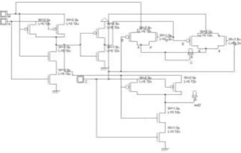
Fig -7: Schematic of 14T full adder circuit
Fig -8: Simulation of 14T full adder
Fig -9: Schematic of 4T half adder circuit
[image:4.595.306.561.56.395.2] [image:4.595.31.295.204.283.2] [image:4.595.308.570.425.576.2] [image:4.595.40.286.491.647.2]© 2019, IRJET | Impact Factor value: 7.211 | ISO 9001:2008 Certified Journal | Page 1413
Fig -11: Schematic of Dadda algorithm based low power [image:5.595.37.289.90.355.2]high speed Multiplier using 4T XOR gate
Fig -12: V/T Simulation of Proposed Multiplier
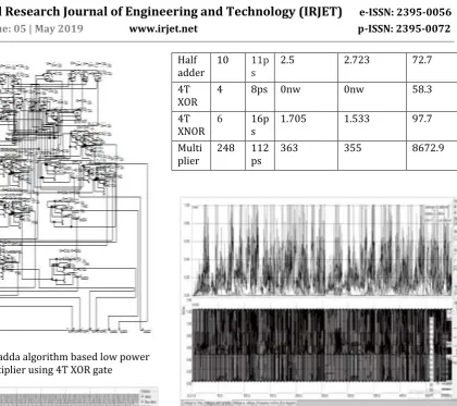
Table -7: Simulation results of proposed multiplier
Circu it No.of
tran sist or
Del
ay Power dissipatio n(V/T Microwatt )
Power dissipation (V/I Micro Watt)
SUFACE AREA(M icromet er2)
AND
gate 6 12p s
2.653 1.965 19.2
Full
adder 14 25ps 3.593 3.04 248.2
Half
adder 10 11ps 2.5 2.723 72.7
4T
XOR 4 8ps 0nw 0nw 58.3
4T
XNOR 6 16ps 1.705 1.533 97.7
Multi
plier 248 112ps 363 355 8672.9
Fig -13: V/I Simulation of Proposed Multiplier
3. CONCLUSION
[image:5.595.36.290.400.577.2]© 2019, IRJET | Impact Factor value: 7.211 | ISO 9001:2008 Certified Journal | Page 1414
REFERENCES
[1] Pranay Kumar Rahi, Rajesh Mehra” CMOS 4-bit Multiplier design & simulation using different foundry” International Journal of Scientific Research Engineering & Technology (IJSRET) ISSN: 2278–0882 EATHD-2015 Conference Proceeding, 14-15 March, 2015
[2] D.Sony” Comparison of Wallace, Vedic and Dadda Multipliers” International Journal of Advance Engineering and Research Development Volume 5, Issue 03, March -2018
[3] S.Narendra, A.Maheswara reddy, S.Saleem , K.M.Haneef ” 14 Transistor full adder circuit using 4 transistor XOR gate and Transmission gate” National Conference on Emerging Trends in Information, Management and Engineering Sciences (NC’e-TIMES#1.0) – 2018.
[4] Radhakrishnan D,” Low-voltage low-power CMOS full adder”, in Proc, IEEE Circuits Devices System, 148, 2001, 19-24.
[5] Shams A.M, Darwish T.K and Bayoumi M.A, “Performance analysis of low-power 1-bit CMOS full adder cells”, IEEE Trans, Very Large Scale Integration (VLSI) Systems, 10 (1), 2002, 20–29.
[6] Bui H.T, Al-Sheraidah A.K and Wang Y, New 4-transistors XOR and XNOR designs, in Proc. 2nd IEEE Asia Pacific Conference, ASIC, 2000, 25–28.
[7] Jin-Fa Lin Hwang Y.T, Sheu M.H and Ho C.C, A Novel High-Speed and Energy Efficient10- Transistor Full Adder Design, IEEE Transactions on Circuits and Systems, 54 (5), 2007, 1050-1059.
[8] Zain Shabbir, Anas Razzaq Ghumman, Shabbir Majeed Chaudhry, A Reduced-sp-D3Lsum Adder-Based High Frequency 4 × 4 Bit Multiplier Using Dadda Algorithm, Springer Science+Business Media New York 2015.
[9] S. Selvi, S. Pradeep,’’ 6 Transistor Full Adder Circuit Using Pass Transistor Logic ’’ Journal of Chemical and Pharmaceutical Sciences, JCHPS Special Issue 1: February 2017.
[10] Hung Tien Bui, Yuke Wang, and Yingtao Jiang, “Design and Analysis of Low-Power 10-Transistor Full Adders Using Novel XOR–XNOR Gates” IEEE transactions on circuits and systems—ii: analog and digital signal processing, vol. 49, no. 1, January 2002.
[11] Muhammad Hussnain Riaz, Tariq Kamal,” Low Power 4×4 Bit Multiplier Design using Dadda Algorithm and Optimized Full Adder” Conference Paper · March 2018 DOI: 10.1109/IBCAST.2018.8312254
”
a d h a k r i s h n a n
D ,
L o w -v o l t a g e
l o w -p o w e r
C M O S