Surface treatment in a cathodic arc plasma : Key step for
interface engineering.
SCHONJAHN, Cornelia.
Available from Sheffield Hallam University Research Archive (SHURA) at:
http://shura.shu.ac.uk/20336/
This document is the author deposited version. You are advised to consult the
publisher's version if you wish to cite from it.
Published version
SCHONJAHN, Cornelia. (2001). Surface treatment in a cathodic arc plasma : Key
step for interface engineering. Doctoral, Sheffield Hallam University (United
Kingdom)..
Copyright and re-use policy
CJTY CAMPUS, PC-HD S i BEET,
SHEFFElOi S' ' !' S'
101 659 919 6
Fines are charged at 50p per hour
ProQuest Number: 10700982
All rights reserved
INFORMATION TO ALL USERS
The quality of this reproduction is dependent upon the quality of the copy submitted.
In the unlikely event that the author did not send a com plete manuscript and there are missing pages, these will be noted. Also, if material had to be removed,
a note will indicate the deletion.
uest
ProQuest 10700982
Published by ProQuest LLC(2017). Copyright of the Dissertation is held by the Author.
All rights reserved.
This work is protected against unauthorized copying under Title 17, United States C ode Microform Edition © ProQuest LLC.
ProQuest LLC.
789 East Eisenhower Parkway P.O. Box 1346
Surface treatm ent in a cathodic arc
plasma - key step for interface
engineering
Cornelia Schonjahn
A thesis submitted in partial fulfilment of the
requirements of Sheffield Hallam University for
the degree of Doctor of Philosophy
Abstract
Advanced Studies
The following conferences and workshops were attended during the stud ies for this thesis:
(I) Elektrochemische and Physikalische Oberflachenbeschichtung, April 1998, Freiberg, Germany
(II) Fourth Sheffield Arc bond Sputtering (ABS) Days, July 1998, Sheffield, UK
(III) 14th International Vacuum Congress, A ugust/ September 1998, Birmingham, UK
(IV) European Materials Research Society (E-MRS) Spring Meeting, Strasbourg, June 1999, France
(V) Fifth Sheffield ABS Days, July 1999, Sheffield, UK
(VI) Institute of Physics Electron Microscopy and Analysis Group Con ference (EMAG), August 1999, Sheffield, UK
(VII) American Vacuum Society (AVS) 46th International Symposium, October 1999, Seattle, USA
(VIII) Sixth Sheffield ABS Days, July 2000, Sheffield, UK
(IX) AVS 47th International Symposium, October 2000, Boston, USA
Publications & Patents
(I) C. Schonjahn, H. Paritong, L.A. Donohue, W.-D. Miinz, R.D. Twesten, and I. Petrov. Influence of Cr+ and Nb+ substrate sputter cleaning on the formation of Tii_xAlxN/steel interfaces generated in a combined cathodic arc/unbalanced magnetron deposition system. Inst. Phys. Conf. Ser. 161 (1999) 75-78
(II) C. Schonjahn, M. Bamford, L.A. Donohue, D.B. Lewis, S. Forder, and W.- D. Miinz. The Interface between TiAIN hard coatings and steels substrates generated by high energetic Cr+ bombardment. Surf. & Coat. Technol. 125 (2000) 66-70 (Young scientist best paper prize awarded by E-MRS)
(III) C. Schonjahn, L.A. Donohue, D.B. Lewis, W.-D. Miinz, R.D. Twesten, and I. Petrov. Enhanced adhesion trough local epitaxy of transition-m etal nitride coatings on ferritic steel promoted by metal ion etching in a combined cathodic arc/unbalanced magnetron deposition system. J. Vac. Sci. Technol. A 18(4) (2000) 1718-1723
(IV) C. Schonjahn, D.B. Lewis, W.-D. Miinz, and I. Petrov. Substrate Ion Etching in a Combined Steered Cathodic Arc-UBM Deposition System: Effects on Interface Architecture, Adhesion and Tool Performance. Surf. Eng. 16(2) (2000) 176-180
(V) C. Schonjahn, A.P. Ehiasarian, D.B. Lewis, R. New, W.-D. Miinz, R.D. Twesten, and I. Petrov. Optimization of In-Situ Substrate Surface Treatm ent in a Ca thodic Arc Plasma: A Study by TEM and Plasm a Diagnostics. J. Vac. Sci.
Technol. A, July/A ugust 2001
(VI) C. Schonjahn, H. Paritong, W.-D. Miinz, R.D. Twesten and I. Petrov. Influ ence of the Interface Composition on the Corrosion Behavior of Unbalanced Magnetron Grown Niobium Coatings on Steel. Submitted for publication in J.
(VII) W. D. Miinz, I. J. Smith, C. Schonjahn, A. P. Deeming, and S. Clapham. PVD Superlattice Structured Hard Coatings Designed for Dry High-Speed Machining. Conference Proceedings, Nantes, June 2000.
(VIII) W.-D.Miinz, C. Schonjahn, H. Paritong, and I.J. Smith. Source combinee, arc cathodique et magnetron desequilibre pour le depot de couche minees (Arc Bond Sputtering : ABS). Le Vide 205 (2000) 297-314
(IX) W.-D. Miinz, D.B. Lewis, P.Eh. Hovsepian, C. Schonjahn, and I.J. Smith. Superlattice structured hard PVD coatings. Surface Engineering 17(1) (2001)
(X) H. Paritong, C. Schonjahn, L.A. Donohue, and W.-D. Miinz. PVD Interface Design by Cathodic Arc Generated High Energy Ion Bombardment. Accepted for publication in proceedings EUROMAT, Munich, September 1999.
(XI) H. Paritong, C. Schonjahn, and W.-D. Miinz. Einfluss der Teilchenenergie von Nb-Ionen beim Atzen von Substraten auf das Korrosionsverhalten nach der Beschichtung, Patent Pending, DPA 100 22 274.9
(XII) A.P. Ehiasarian, K. Macak, C. Schonjahn, R. New, and W.-D. Miinz. In fluence of the Ion Flux Density on the Efficiency of the Metal Ion Etching Process in Cathodic Arc Discharges. Accepted for publication in proceedings EUROMAT, Munich September 2000.
Acknowledgement
Many people to whom I wish to express my gratitude contributed to the present work. First I would like to thank my director of studies Professor W.-D. Miinz who gave me the chance to carry out this research project, for his supervision involving some heavy but finally always fruitful discussions and encouraging and helping me to gain international experience. I am also very grateful to my supervisor Dr D.B. Lewis who always had an open ear for all sorts of problems, for motivating me when I needed it most and all his valuable ideas and advice. My gratitude yields
Professor J.M. Rodenburg for the same reasons but in addition for teaching me TEM and English and making lunch very enjoyable by a refreshing humour. The latter is also true for P. Slingsby, T. Hudson and Dr M.C. Simmonds. I also like to thank all other MRI staff in particular S. Porter, P. Allender and C. Shaw for all technical support and friendly chats. The same applies to all members of the Surface Engineering Group and Bodycote SHU Coatings Ltd. staff. Specifically I like to thank R. Day, G. Robinson and C. Sellars for always giving me a hand and teaching me English heritage, English language and South Yorkshire, respectively. I also thank Dr I. Smith for all the lifts he gave me but more im portantly for always being there when nobody else was and there was trouble with the ABS machine. For helping me at the machine my thanks goes to Dr P. Hovsepian, Dr K. Macak and
A. P. Ehiasarian. Besides machine time I also shared many pub and party hours with A.P. Ehiasarian, H. Paritong and many other fellow students whom I like to thank for all that happy hours. Special thanks go to M. Lembke and A. Crecelius
who helped me a lot sharing my problems and providing me accommodation.
I also like to thank all members of Professor J.E. Greene’s Thin Film Group for their hospitality and very warm welcome. In particular I like to thank V. Petrova
and S. Kodambak who made me feel so comfortable in Illinois th at I always found it hard to leave.
I like to thank Dr T. English and his Surface Analysis Group at Corus for teaching me English, British Humour and a little bit AFM and surface analysis.
Many thanks to Dr H. Kheyrandish and Dr S. Romani from MATS UK for inviting me to their Lab, teaching me some SIMS and SNMS and our discussions.
Contents
1 Introduction
5
2 Literature review
8
2.1 Selected PVD techniques for transition metal nitride deposition . . . 8
2.1.1 B a s ic s ... 8
2.1.2 Magnetron sputter ion plating ... 11
2.1.3 Cathodic arc (CA)-ion plating/CA -m etal ion e tc h i n g 13 2.1.4 The ABS (arc bond sputtering) technology ... 15
2.2 A dhesion...17
2.2.1 D efinitions... 17
2.2.2 In te rfa c e s ... 19
2.2.3 Dependence of adhesion on the interface type ...22
2.2.4 Adhesion measurement methods for hard coatings ...27
2.3 Film growth and microstructure e v o lu tio n ...29
2.3.1 Structure evolution of polycrystalline f ilm s ...29
2.3.2 E p i ta x y ...32
3 Experimental methods
36
3.1 Coating d e p o s itio n ...363.1.1 Substrate preparation ... 36
3.1.2 Deposition p r o c e s s ...38
3.2 Topography of surfaces ... 42
CONTENTS
3.2.2 Atomic force microscopy (A F M )...42
3.3 Structure and phase analysis ... 43
3.3.1 X-ray diffraction ( X R D ) ... 43
3.3.2 Transmission electron microscopy (T E M )... 43
3.4 Measurement of the elemental distribution across interfaces in the scanning transmission electron microscope . . 44
3.4.1 Scanning transmission electron microscope (S T E M )...44
3.4.2 S T E M -E E L S ... 45
3.4.3 ST E M -E D X ...47
3.5 Etch rate d e te rm in a tio n ... 47
3.6 Stress measurements by X-ray diffraction... 47
3.6.1 Basic p rin cip les...47
3.6.2 Bragg-Brentano g e o m e try ...48
3.6.3 Glancing angle m e th o d ...49
3.7 Determination of practical a d h esio n ...51
3.7.1 Scratch t e s t ...51
3.7.2 Rockwell C in dentation...51
3.8 Determination of tool life ...52
4 Substrate surface modification by ion bombardment
54
4.1 In tro d u ctio n ...544.2 R esu lts...54
4.2.1 Initial substrate surface ... 54
4.2.2 Influence of ion species ... 57
4.2.3 Influence of Cr-ion e n e r g y ... 72
4.2.4 Influence of exposure time to Cr-ion bombardment ... 78
4.2.5 Influence of Ar pressure during Cr-ion b o m b a rd m e n t...80
4.2.6 Influence of arc current used for Cr-ion bombardment . . . . 82
4.3 D iscussion... 84
4.3.1 Influence of ion species ... 84
CONTENTS
4.3.3 Influence of exposure time to Cr-ion bombardment ...94
4.3.4 Influence of Ar pressure during Cr-ion b o m b a rd m e n t... 95
4.3.5 Influence of arc current used for Cr-ion b o m bard m en t... 96
4.4 S u m m a r y ... 96
5 Microstructure of UBM deposited transition metal nitrides
98
5.1 In tro d u ctio n ...985.2 R esu lts...98
5.2.1 Microstructure of TiAIN grown on amorphised metal surfaces 98 5.2.2 Microstructure of TiAIN grown on oxidised su rfa c e s...99
5.2.3 Microstructure of TiAIN grown on clean metal surfaces with preserved crystalline o r d e r ...101
5.2.4 Microstructure of TiAIN grown on locally clean surfaces . . . 104
5.3 D iscussion... 109
5.3.1 Microstructure of TiAIN grown on amorphised surfaces . . . . 109
5.3.2 Microstructure of TiAIN grown on oxidised surfaces ...110
5.3.3 Microstructure of TiAIN grown on clean crystalline surfaces . I l l 5.3.4 Microstructure of TiAIN grown on locally clean surfaces . . . 113
5.4 S u m m a r y ...114
6 Mechanical properties of coated systems
115
6.1 In tro d u ctio n ... 1156.2 R esu lts... 115
6.2.1 Stress ... 115
6.2.2 Practical adhesion ... 117
6.2.3 Life time of coated tools in dry high-speed machining tests . . 120
6.3 D iscussion...120
6.3.1 Practical adhesion and its relation to interface properties . . 120
6.3.2 Relation between film stress and m ic ro stru c tu re ... 123
CONTENTS
6.3.4 Relationship between practical adhesion and tool life in dry
high-speed machining ...125
6.4 S u m m a r y ...127
7 Conclusions
128
Bibliography
130
List of Figures
147
A Nb-ion bombardment for corrosion protection-initial results
156
A .l In tro d u ctio n ... 156A.2 Experimental m e th o d ...157
A.2.1 Nb-ion treatm ent p ro c e d u re ...157
A.2.2 Potentiodynamic p o la ris a tio n ... 157
A.3 Results & D iscussio n ...158
A.3.1 Stainless s t e e l ... 158
A.3.2 Low carbon s t e e l ...162
A.3.3 B ra ss... 163
B TEM sample preparation guide
165
B .l Preparation of cross-sections... 165B.2 Preparation of samples for in plane im a g in g ...167
Chapter 1
Introduction
W ithin the last decades a fast development in a range of physical vapour deposition (PVD) techniques for modifying the surface of engineering components has taken place. This led to a new field of surface engineering - the design of a composite system (coating plus substrate) that produces a performance which cannot be achieved by either the coating or substrate materials [1].
One application for these composite systems is the wear and oxidation protec tion of cutting tools, in particular under very harsh conditions like dry high speed machining.
Chapter 1: Introduction
in the range of a few nanometres for graded interfaces. This means that interface analysis is a challenge for most analytical techniques. Therefore the first aim of the work presented here was to establish a procedure, which is suitable for the charac terisation of the TiAIN/ steel interfaces with respect to their chemical composition and microstructure.
To engineer interface properties successfully, which was the main objective of this project, the influence of process variables for coating deposition has to be known. Various PVD processes have different limitations. Therefore a brief review about selected PVD techniques is given in Section 2.1. Special attention is paid to the ABS (Arc Bond Sputtering) technique, which combines two PVD techniques in one coating unit, namely unbalanced magnetron sputtering (UBM) and cathodic arc (CA) evaporation. Main driving force for this development was the superior adhesion usually observed for arc deposited coatings in comparison to the much smoother sputter deposited films. The main emphasis of this project was to explore and optimise the potential of a cathodic arc source for interface engineering. An industrial sized ABS coating unit (Hauzer 1000-4) was used for all experiments to ensure a direct transfer of the experimental results of this study to commercial applications.
The standard PVD process consists of ex-situ pre-cleaning of substrates, load ing to the vacuum chamber and pump down, substrate heating, in-situ substrate cleaning, interface formation, film deposition and substrate cooling and unloading [3]. In-situ substrate cleaning is the key step for interface formation because it may alter the original substrate surface considerably as discussed in detail in Chapter 4. Likewise, the interface strength depends on the microstructure of the coating as de scribed in Section 2.2.3. Therefore a brief overview about m icrostructure evolution is given in Section 2.3.
Chapter 1: Introduction
Chapter 2
Literature review
2.1 Selected PVD techniques for transition metal
nitride deposition
2.1.1 Basics
The PVD (physical vapour deposition) method is the deposition of coatings by condensation of vapour in vacuum. The deposition process consists of three main steps, which are independent of the particular deposition technique [6]. These are
(I) vaporisation of the material to be deposited,
(II) transport of this material towards the substrate,
(III) film growth [3].
Vaporisation
Chapter 2: Literature review
Transport
During the transport the vapour atoms can collide elastically or inelastically with gas atoms. Elastic scattering influences mainly the distribution of the vapour in the deposition chamber and therefore film-thickness uniformity. Inelastic collision pro cesses, such as ionisation, determine the flux of activated species (e.g. ions). Because of the significant effect of gas presence one can classify the following processes:
(I) vacuum processes (line-of-sight movement of metallic particles),
(II) processes in an inert gas atmosphere (scattering of metallic particles),
(III) reactive processes (formation of compounds) [8].
Film growth
Film growth on the substrate surface is influenced not only by the substrate material and temperature, but also by the fluxes and energies of all bombarding species. The following dominant parameters have to be considered [3]:
(I) the flux and energies of metallic particles,
(II) the flux and energies of reactive gas particles, and
(III) the flux and energies of ions (relevant for ion plating, see below).
The term ion plating is applied to atomistic film deposition processes in which the substrate is subjected to a flux of high energy ions sufficient to cause appreciable sputtering before and during film formation ([9],[10], and [11]) 1 , independent on the source of the ions. Particle bombardment effects include
(I) modifying the substrate surface (cleaning, defect formation),
Chapter 2: Literature review
(II) momentum transfer processes in the surface region (sputtering, desorption, recoil implantation, defect formation),
(III) addition of heat to the surface region,
(IV) formation of secondary electrons that can affect reactions [13].
Various PVD techniques have been developed combining different vaporisation-, transport-, and film growths conditions. These techniques vary in their deposition rate, the possibility of alloy deposition, and differences in coating microstructure and adhesion. So called structure zone models were developed to correlate the microstructure of the coating and process parameters. The dependence of the mi crostructure of evaporated films on the substrate tem perature is given by the struc ture zone model from Movchan and Demichishin [14]. It classifies the microstructure of metallic coatings as a function of homologous tem perature T /T m (where T stands for substrate tem perature and Tm for the melting point of the coating material) in three groups (zones). The microstructures reaches from porous columnar (zonel) at homologous temperatures < 0.3 to fully dense equiaxed grains for T /T m > 0 .5 . The Movchan and Demichishin model was extended by Thornton by adding a sec ond axis to account for the effect of argon working gas pressure in sputtering [15]. Messier [16] replaced the pressure axis with a substrate bias axis therefore, intro ducing the effect of ion energy. A third axis accounting for the thickness of the film was also introduced. In addition to thermal and ion bombardment induced mobility ’’chemically induced mobility” should be considered. The chemically induced mobil ity refers to a control over the vapour species involved, their adsorption-desorption characteristics, and thus the ad-atom bond strength. Therefore it would account for surface chemical interactions [16].
Chapter 2: Literature review
2.1.2 Magnetron sputter ion plating
In a sputter process coating material is dislodged and ejected from the solid surface due to momentum transfer associated with surface bombardment by energetic par ticles (high energy ions or neutrals). A certain energy (20 to 40 eV) is required for sputtering to occur. Above this threshold energy the sputtering yield (i.e. number of emitted target atoms per incident particle) increases with increasing energy until it reaches a maximum in the energy range of 5 keV to 50 keV [17]. For a particle of a given energy and incidence angle the sputtering yield depends on the mass of the target atoms, the degree of crystalline order and crystal orientation of the target, and its surface binding energy. An advantage of the sputter technique is that the chemical composition of sputtered coatings is often the same as the composition of the target, even when the components differ considerably in their sputtering yield
[6],
In glow discharge sputter deposition the source of coating m aterial (the target) is bombarded by working gas ions. Some working gas atoms are ionised due to the collision with secondary electrons and then accelerated to the negatively biased tar get. When these highly energetic ions hit the target surface momentum transfer can initiate collision cascades, such th at target atoms are ejected from the target surface. In addition, various other events can take place at the target surface and within the target. These include backscattering, photon generation, desorption of gas atoms from the target surface, local heating, implantation, compound formation, amor- phisation, and the creation of point defects, as shown in Figure 2.1. Furthermore, secondary electrons can be emitted. Those are necessary for further ionisation of the working gas in order to sustain the glow discharge.
Chapter 2: Literature review
Primary ions
B ackscattered particles S econdary electron
h v © G as desorption Modification of
surface properties
Amorphisation Chem ical surface
reactions Topography
ch an g es Com pound
formation Collision
cascad e
Implantation i\| Thermal
7 j spike-:!:
: Point':'
| defect iShock
Sputtering, energy and m om entum ::::: transfer, annealing, enhanced diffusion
F igure 2.1: Possible ion-target interactions (from [18]).
to a higher current density. The latter one gives rise to an increase in deposition rate in comparison to a conventional diode sputtering arrangement [19].
Chapter 2: Literature review
2.1.3 Cathodic arc (CA)-ion plating/C A -m etal ion etching
The evaporated species are produced by striking one or more electric arcs on the surface of the material to be evaporated (cathode of the arc discharge). The evapo ration is a consequence of high local cathode surface temperatures. The evaporated material is ionised by collisions with electrons and then accelerated away from the cathode due to the nonuniform potential distribution and plasma expansion [3]. The plasma is highly ionised up to 100% and contains macroparticles (also called droplets) in addition to electrons, ions, and atoms, as shown in Figure 2.2a.
D ro p le t w ith lim ite d a d h e s i o n
A n odi
Metol
•v ■ * D in t! Ploim o Region
0$'+r“ '» ' 1
Neutrol n V o p o r
y v
— ■ •*© M etal lone
\\ ®
M lc ro d ro p ltti
(a)
(a)
IbJ
(d )
o
D ro p le t t
~
\ L
la
M r
E a rly s t a g e n o d u le - lik e g ro w tli d e f e c t
C o m p r e s s tv e f o r c e s
M o m e n t o f lo s s o f n o d u le - lik e d e f e c t
, D is h like g ro w lti d e f e c t
R efill m a te r ia l a f te r f u rth e r film g ro w th
(
6
)F igure 2.2: Cathodic arc evaporation: (a) cathode spot region of a vac uum arc showing neutral, ion, and microdroplet emission (from [24]); (b) effect of weakly bound microdroplets on hole generation in the coating (from [25])
[image:24.613.108.516.260.490.2]Chapter 2: Literature review
Cr m e l
m*
0
IkV]
li l i f t r II*F» Ii*F»
s ik itr a te I m l i r y
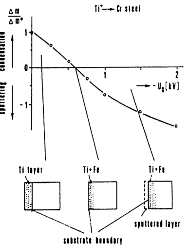
F igure 2.3: Effect of the substrate bias on substrate surface modification by metal ion bombardment . Prom [3].
current. At low arc currents (below 50 A) the main loss of cathode material occurs in the form of ions (greater 50%) [29].
[image:25.612.108.304.84.336.2]Chapter 2: Literature review
C * 0 l^ i— i s i— i n| E R 1
N
pro
pro
n]
F igure 2.4: Schematic diagram of the combined UBM /CA four-target deposition system used in these experiments.
cleaning or metal ion etching.
2.1.4 The ABS (arc bond sputtering) technology
The ABS technology was developed in order to combine the advantages of the arc technology (i.e. good adhesion due to metal ion etching) with the versatility of material selection given by the application of magnetron sputtering for deposition of smooth coatings [31]. The ABS technology is realised in the Hauzer Techno
Coating Europe B. V. H TC 1000-4 combined CA/UBM system (see Figure 2.4) [31] by moving the permanent magnets in a manner shown in Figure 2.5. The typical deposition sequence consists of the following steps:
(I) pump down,
(II) heating and degassing,
(III) target sputter cleaning,
[image:26.613.206.407.53.266.2]Chapter 2: Literature review
UBM-Mode
Arc-Mode
Figure 2.5: Cathode design for alterative arc and UBM modes: 1 - target; 2 - permanent magnets; 3 - magnetic yoke; 4 - magnetic coils.
(V) UBM film deposition,
(VI) cool down.
Of special interest here was CA metal ion etching prior to the deposition of TiAlN. Different cathode materials (metal ions) may be used. In order to generate a graded interface (see Section 2.2.2) the use of a TiAl cathode would seem to be appropriate. However, the low melting point of this m aterial results in many large droplets [4]. An investigation of droplet number and size for different materials was carried out previously ([4], [5]). The maximum droplet diameter decreases rapidly with increasing melting point 2 . A higher vapour pressure may also result in a further decrease of droplet size since even solidified droplets may shrink due to sublimation during the flight or after arrival at the substrate surface ([4], [5]). Therefore, Cr seems to be well suited as target material, not only due to its high melting point but also because of its high vapour pressure.
In fact, a reduction of roughness (by reduced droplet size and number, hence, less pronounced and fewer growth defects) by using Cr instead of TiAl led to a doubling of the life time in dry drilling tests carried out in cast iron [32].
Chapter 2: Literature review
2.2
Adhesion
2.2.1 Definitions
Fundamental adhesion refers to nature and strength of the binding forces between
two materials in contact. It is defined as the summation of all interfacial intermolec-
ular interactions between the contacting materials [33]. These binding forces can be classified as follows [34, 35]:
(I) primary valence type or chemical bonding (ionic, covalent or metallic),
(II) pseudo primary valence type (hydrogen bridge bonding),
(III) secondary valence type (Debye, Keesom and London dispersion forces - collec tively known as Van der Waals forces).
The last two types of forces are classified in [35] as physical bonds. Chemical bonds reveal a relatively strong interaction energy between 1 1 0^ and 1 0 0 0^ for metallic bonds and covalent or ionic bonds, respectively. The physical bond strength is rather weak with less than 5 0 The forces of adhesion resulting from these energies vary from 5 0 0 ^ 2 ’m the case of hydrogen bonding to 5 0 0 0 ^2 and more for chemical bonds [36].
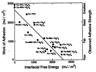
Adhesion can also be expressed in thermodynamical terms. Thermodynamic adhesion signifies the change in free energy when an interface is formed, and is expressed as
Wa — 7si + 7S2 ~ 7siS25 (2.1)
where Wa is the work of adhesion 3 and 751 and 752 represent the surface free energies of material 1 (substrate) and material 2 (film), respectively. The interfacial free energy is written as 75152 [33]- This shows th at the work of adhesion increases when the interfacial free energy decreases. It means th at more work is required to separate strongly bounded low energy interfaces than weekly bound high energy
Chapter 2: Literature review
ones [37]. The relation between interfacial free energy and work of adhesion for various ceramic-metal systems is shown in Figure 2.6.
3000
.
CM
2000
c
o ’c oO
JZ
3
F*>15Cr/AljOg OMONi/AljC^
0 F t/F eO
-
•
P«C r/AI2p >> taFe/FCgC • Pt/AIjdj
F*-40NH0Cr/AljO,
F*5M0/AljO,
tN/AIjQ,
Au/AI20 ,#
AO/AIjO,^Cu/AljO, • Ft-40NI/Al203 • M/AIjOj
Interfacial Free Energy (mJ / m )
§
UJ CDC
£
I ®
!
3
jc
3
I |
(D
CO
8
F igure 2.6: Inverse correlation between the thermodynamic work of adhesion and the interfacial energy for various ceramic-metal systems (from [37]).
[image:29.612.139.474.112.363.2]Chapter 2: Literature review
2.2.2 Interfaces
Overview
The transition region from the substrate material to the coating material is the
interface region. It can be classified in abrupt-, mechanical-, diffusion-, compound-,
pseudo-diffusion-, and reactively graded interfaces, or as a combination of them [38] (see Figure 2.7).
Weiss [35] prefers a different classification th at distinguishes between a monolayer by monolayer interface, a diffusion interface, an intermediate phase interface, a physical bond interface, and an interlocking interface.
The type and extent of the interface region depends on the deposition process, and it influences the adhesion of the coating to the underlying substrate. A certain depth of the interface region may result in an increase of the adhesion as well as
a graded interface. In the latter case the stress level can be reduced by avoiding
abrupt changes in interplanar spacing. A particular interfacial composition may be beneficial in order to guarantee a better compatibility between substrate and coating material [39].
Mechanical aspects
An interface on a rough surface where the rough surface is filled to give rise to me chanical interlocking is called a mechanical interlocking interface. The interlocking sites can vary from mechanically machined dove-tails, grooves to micro-roughness produced by grit blasting [35]. There are three different mechanisms of mechani cal interlocking involved. These are an increased surface area, friction locking, and dovetail locking [35] (see Figure 2.8).
Elemental Distribution Consideration
• Abrupt interface or physical bonding interface: These types of interfaces are both characterised by an abrupt change from the substrate m aterial to coating
Chapter 2: Literature review
Interfacial void
B B
Abrupt interface
Void
Mechanical interface
Voids
A + B
A /
© ©^ 1 Interphase
© © J material
B B
Diffusion (graded) interface
A A
o
Voids
0 Microcracks
B B
Com pound interface
• A
• •
B . A atom s in B surface
from recoil implantation
"Pseudodiffusion" interface
F igure 2.7: Schematic drawing of different types of interfacial regions (from [38]).
interface is considered to be a two-dimensional plane. The abrupt interface defined in [38] is formed when only weak chemical reactions are involved and if no bulk diffusion is observed. Quasi-interaction free interfaces are formed if both the coating and the substrate material bonding are of the covalent type [40].
• Diffusion; pseudo-diffusion and intermediate phase interfaces: All these inter faces are characterised by a gradual change in chemical composition. This can be either caused by diffusion, by “grading” the deposition m aterial from one material to the other, or by recoil implantation during concurrent or subse
quent ion bombardment (pseudo-diffusion interface). If separate phases are
in-Chapter 2: Literature review
coating coating coatin g
surface area increase friction locking dove tail lock ing
-TLTLTL
-7_ r z _ n _ j-substrate substrate substrate
F igure 2.8: Different types of mechanical interlocking (from [35]).
terface is created. This type can be expected for interfaces between metallic and ionic hard materials [40]. These interfaces are most likely to be formed by ion assisted deposition.
• Compound, reactively graded interfaces: The compound interface requires dif fusion along with chemical reaction to form a compound interfacial region. The compound containing interface can also be formed by controlling the availabil ity of reactive gases during the reactive deposition. These interfaces are most likely to be formed by ion assisted deposition and nitriding.
Structural matching
The interface might be crystalline/amorphous or crystalline/crystalline (single- or
polycrystalline). If both materials in contact are crystalline they can either have a
different (for example b.c.c/f.c.c interface) or similar bravais lattice (f.c.c/f.c.c). In
the latter case, despite differing lattice parameters for heterophase interfaces, the
two layers of neighbouring phases might fit together by generating misfit dislocations (semi-coherent interface) or introducing stress in the coating m aterial (coherent in terface). This type of interface is characterised by almost perfect chemical bonding. Metallic hard materials are able to form such coherent or semi-coherent interfaces with metals [40]. Coherent and semi-coherent interfaces are observed when the film
growth is epitaxial. It is possible to find semi-coherent interfaces or coherent inter
Chapter 2: Literature review
2.2.3 Dependence of adhesion on the interface type
Mechanical aspects
An increased substrate surface roughness may result in mechanical interlocking, where fracture along this interface requires changing stress tensors. Thus, the prac tical adhesion can be high [38]. An example of mechanical interlocking are diamond- metal composite coated cemented carbide tools [41], where “anchoring roots” are
formed on the interface. It is also reported th at the increased adhesion of Si0 2
films, deposited by radio-frequency (RF) sputtering onto stainless steel substrates, is due to the formation of microvoids in the interface layer. This allows mechanical interlocking between the coating and the substrate. The microvoids were induced by extended ion bombardment [42].
If the cavities resulting from surface roughness cannot be filled the adhesion will be lower due to a lack of contact and interfacial voids. For example, Koski [43] stated that with decreased substrate roughness (Ra = 116nm, 77nm, 27nm) the adhesion was improved (measured with cantilever and 3 point bending test) for a
DC planar magnetron deposited coating. Liu et al. [44] found the same tendency on
ion plated CrN coatings. According to Carvalho et al [45] a smoother surface leads
to a longer fatigue life for low contact stress. At higher contact stress the surface roughness seems to have only very little influence.
Elemental distribution consideration
Improved practical adhesion (scratch test) was found when a Ti interlayer was de
posited on AISI D2 steel prior to TiN deposition using a hollow cathode discharge
(HCD) ion plating technique [46]. Here it was reported th at depth profiles by sec
ondary ion mass spectrometry (SIMS) indicate th at the adhesive strength of the
coating/substrate interface increased with increasing interdiffusion depth. Diffusion is not always beneficial for a high adhesive strength, as in case of carbon nitride thin films. Poor adhesion on tool steel was found owing to diffusion of nitrogen or carbon
Chapter 2: Literature review
also reported by Helmersson et al. [48] that a Ti interfacial layer deposited above
400 Xj reduces the adhesion of a TiN coating on HSS (high-speed steel), whereas
below this tem perature it has a beneficial influence on the adhesion. The reduced adhesion at higher tem perature is explained to be the result of TiC formation.
A detrimental effect of compound formation on the adhesion is frequently re ported for the so called duplex treatm ent ([49],[50]), which comprises plasma nitrid- ing of the substrate prior to hard coating deposition when the nitride-layer includes
a compound zone (e — Fe2_3N and 7' — Fe4N) [51]. Nitriding of the substrate is
performed to increase the load bearing capabilities in order to support a tribological coating under applied stresses [49], to reduce oxidation [52], and for being beneficial for the adhesion of hard coatings ([53],[54],[55],[56] and [57]). The latter is only the case when no compound layer, resulting from the nitriding process, is formed [58]. A reduced practical adhesion of the hard coating on a compound containing surface is explained by the brittleness of the compound layer, compared to a non-nitrided sub strate surface. D’Haen also [59] reports bad adhesion of Ti-TiN coatings deposited
on plasma nitrided AISI 304 steels caused by the formation of CrN precipitates. The
explanation for the bad adhesion is, according to D ’Haen, the brittleness, which is a result of CrN formation.
As mentioned above Ti is used as a bond layer for TiN coatings, so too is Cr. A Cr bond layer is followed by a graded CrN interlayer, which is gradually changing to a Cr-Ti-N layer before the actual coating - the Cr-Ti-N layer - is deposited. This results in an improved adhesion when compared with the adhesion of CrN or Cr-Ti-N deposited directly onto the steel substrate [60].
The formation of CrN during a low pressure plasma treatm ent of AISI 440 C
and AISI 316 L was observed by Goning et al. [61] using X-Ray photoelectron
Chapter 2: Literature review
I
B
<3
(a). (b)
Figure 2.9: Coherent interfaces with no mismatch (strain free inter
faces): (a) different chemical composition, same crystal structure; (b) different composition and crystal structure (from [62], page 143).
Structural matching
The work of adhesion or interface strength, as given by equation 2.1 in Section 2.2.1, depends not only on the free energies of the materials in contact but also on the
interfacial energy 75152- There are two factors which can contribute to the interfacial
energy; a compositional 7° and a structural component 7s as expressed by equation
2.2.
75152 = 75152 + 75152* ( 2 -2 )
If there is no mismatch between the two materials as shown in Figure 2.9 (for example
two phases a and ft which differ only in their composition) the only contribution to
the interfacial energy is the compositional component 4 .
Therefore, in that case the interfacial free energy is low. Typical values for
coherent interfaces are 75152 < 2 0 0 ^ [62]. In semi-coherent lattices the mismatch
can be accommodated by elastic strain in the film or in form of misfit dislocations
as shown in Figure 2.10 a and 6, respectively.
An expression for the misfit dislocation energy 7^ 52 was formulated by van der
Merwe [65] and is presented in equation 2.3
Tsisa = + A - V T + V - A In 2A n/TTA ? - 2A2), (2.3)
Chapter 2: Literature review
H d» b"
(a) (b)
F igure 2.10: Interfaces with small lattice mismatch: (a) with co herency strains; (b) with misfit accommodation via a series of edge dislocations (from [62], page 144 and 145).
where
A = 2tt5Cs
c
8 1- 1/1 _ |_1
1—^2 '(2.4)
(2.5)
H i H 2
\i is the interfacial shear modulus, and /ii and fii are the shear moduli of phase 1 and
phase 2, respectively. Accordingly, z/i and v2 are the Poisson ratios for these phases,
and ai and a2 are the lattice parameters and 8 is the misfit. For small differences
in the lattice parameters 8 is given by equation 2.6
Ql ~ &2
a>i (2.6)
. The Cs term in equation 2.2.3 is an effective elastic constant th at accounts for
elastic interactions within each crystal, whereas /i accounts for such interactions across the interface. For a small misfit it can be energetically favourable to strain
the film. The elastic strain energy E e[ can be calculated using equation 2.7 [37]
/ii(l - Vi)L82
E ei = (2.7)
1 — 2Vi
L is the thickness of the film (phase 1).
Chapter 2: Literature review
F igure 2.11: Incoherent interface as it occurs for very different pat terns of matching atoms or similar patterns but intertatomic distances > 25% (from [62], page 147).
the strain energy increases. When it reaches the value of the misfit dislocation en ergy dislocations are formed. That critical thickness depends not only on the misfit but also on the elastic constants of the film. Elastic strain energy or misfit disloca tion increase the interfacial energy according to equation 2.2. Typical values of the
interfacial energy are given in [62] to be in the range of 2 0 0 ^ < 75152 < 5 0 0 ^ .
According to Howe [37] the upper limit is 8 0 0 Howe [37] gives a comparison of the structural and the compositional components of the interfacial energy for two f.c.c crystals with different lattice parameters as a function of tem perature for two
different misfits of 0.2% and 2%. It is shown th at the compositional contribution 7°
dominates for the smaller misfit but at the large misfit the structural contribution
7s can be more than twice the value for 7C. The structural contribution depends
much less on tem perature compared to the compositional contribution, which drops sharply at increased temperatures. Hence, at high tem peratures the structural com ponent becomes more dominant.
In incoherent interfaces the misfit is evenly spread out along the entire interface,
as shown in Figure 2.11. For such interfaces the interfacial energy is said to be in
the range of 8 0 0 ^ < 75151 < 2 5 0 0 ^ [37] or between 5 0 0 ^ < 75151 < 1 0 0 0 ^
Chapter 2: Literature review
The effect of structural matching on practical adhesion of transition metal ni trides on steel or carbides will be reviewed next. However, only few data are avail able because epitaxial growth can only occur under certain conditions (substrate
and deposition related), as described in more detail in Section 2.3.2. For exam
ple, Helmersson et al. [48] found an increased practical adhesion of TiN (scratch-
test) when the HSS substrate surface was covered with a thin FeO (NaCl structure
flFeO = 0.431nm) layer instead of Fe2 0 3 or Fe30 4. They concluded that the in
creased adhesion could be a result of structural matching. On the other hand, in
[66] poor adhesion (scratch-test) of a TiN coating deposited directly on to austenitic
stainless steel without titanium underlayer was reported, in spite of the local epi taxial growth of TiN on the substrate (with a Ti interlayer epitaxial growth has not been observed). However, in [67] it has been suggested th at this could be due to
the stable native Cr20 3 of the substrate (therefore less stable CrN, which provides
chemical bonding, is not formed). The same problem occurs in case of TiN directly deposited to HSS [67] as substrate. But the adhesion is better when compared to
TiN on stainless steel. In case of stainless steel AISI-304 the misfit is larger (see Ta
ble 2.1) and epitaxial growth is apparently insufficient to compensate for the poorer
chemical bonding of nitrogen to the substrate. Therefore, it seems th at epitaxial growth is of advantage for practical adhesion in general. However, epitaxial growth process conditions may imply other parameters th at result in a lower practical ad hesion value due to changes in the compositional component of the interfacial free energy.
2.2.4
Adhesion measurement m ethods for hard coatings
Introduction
Chapter 2: Literature review
• scratch test ([6 8, 69, 2, 70, 71]),
• indentation test ([72, 71, 73, 74]),
• laser spallation ([71, 75, 76]),
• surface acoustic wave methods ([77, 78]), and
• fatigue methods ([45, 79]).
Several review papers are available about the subject ([80], [81],[82]).
Here, only the Scratch test will be considered in more detail, as it is the most
commonly used test. Besides the Rockwell indentation test [83], which provides
qualitative information 5 , it is the only test available for this project.
Scratch-test
The Scratch-test is a widespread method to judge practical adhesion. In the Scratch
test a Rockwell C diamond is drawn over the sample surface under a stepwise or continuously increasing normal force. The resulting damage can be observed either employing an optical microscope, measuring the frictional force or by using the acoustic emission correlated to the appearance of certain failure modes (fairly good correlation is only given in the case of thin coatings on soft substrates [71]). A critical load value is defined, but there is more than one definition of this value. For example, the critical load is often referred to the load at which the coating is removed in a regular way along the whole channel length. There are approaches to relate the work of adhesion to the critical load but the applied models are not universal applicable. This is not only because of the complex stress field generated by the moving stylus but also due to a number of extrinsic parameters, like residual stress in
the coating or the coating thickness. If, for example, the coating is under compressive
stress the critical load is decreased because the effective stress is the summation of
Chapter 2: Literature review
the residual compressive stress and the stress generated by the moving indenter. Adhesive failure (spalling or buckling) occurs when the elastic strain energy stored in the coating exceeds about twice the surface energy required for the generation of a crack within the interface between coating and substrate. This means, the load at which adhesive failure is observed is determined by the ratio between elastic strain and surface energy. This ratio, and therefore the critical load, depends on the coating thickness [84].
2.3 Film growth and microstructure evolution
2.3.1 Structure evolution of polycrystalline films
Work about this subject is often limited to certain deposition techniques and ma terial classes. This Section summarises general aspects involved in microstructure evolution independent of the detailed deposition parameters. This Section is mainly based on a recent review paper by Thompson [85].
The following key process are involved in the microstructure evolution:
(I) nucleation of isolated crystals,
(II) growth of nuclei,
(III) impingement, grain boundary formation, and
(IV) thickening.
The first three steps determine the initial grain structure. The last process can lead to further grain structure evolution in two fundamentally different ways, depend
ing on the mobility of the grain boundaries. In case of immobile boundaries the
Chapter 2: Literature review
Nucleation
The nucleation rate I is given by
7 = /0i2ne=^ a , (2.8)
where I 0 is a tem perature and deposition-flux-independent constant, R is the flux
of atoms arriving at substrate surface, k is Boltzman’s constant and T is the tem
perature of the substrate. AGn is the energy of formation of a cluster of size n,
where n is the critical cluster size. For PVD processes n has a low integer value,
often only one (so that the minimum stable cluster size is two). Because the de gree of supersaturation decreases with increasing T, as T increases, n increases (eg.
form one to three) and AGn increases, so th at the tem perature dependence of the
nucleation rate becomes stronger at higher temperatures. It is generally found that
the nucleation rate decreases with increasing tem peratures. It is im portant to note
that selective nucleation can occur when specific nuclei orientations will minimise surface and interface energies.
Growth of nuclei
Stable nuclei can grow to form islands. Again, the growth of islands with spe cific surface- and interface-energy minimising crystallographic orientations will be favoured.
Impingement, grain boundary formation, and grain growth
Chapter 2: Literature review
they first make contact. This results in substantial strain if there is no sliding at the island/substrate interface.
Grain growth can occur in order to reduce grain boundary energy. Interface and
surface energy affect the grain growth, which leads to texture development. Crystal- lographic orientations which minimise the sum of interface and surface energy are favoured. On amorphous substrates surface energy minimisation does not favour growth of grains with specific in-plane orientations. However, for polycrystalline films on single crystal substrates the interface energy depends on the in-plane ori entation of the grain and grain growth is expected for films composed of grains with
three-dimensionally constraint or epitaxial orientations. In addition grain growth
can favour orientations which provide a strain minimisation. Grain growth can be suppressed by impurities (oxide formation), leading to smaller deposited grain sizes and immobile grain boundaries for materials which would have mobile grain boundaries, when deposited under clean conditions.
Thickening
Once a continuous film has formed through nucleation, growth and coalescence thickening is normally expected to occur via epitaxial growth on preexisting grains, even at quite low temperatures. However, re-nucleation due to impurities can oc cur preventing epitaxial growth. This was demonstrated by the incorporation of
small amounts of Y ttrium in Ti0.43Al0.52Cr0.03Y0.02N films, which leads to a fine
grained near equiaxed microstructure in contrast to the conventional columnar
Tio.44Alo.53Cro.03N coating morphology ([8 6] and [87]). A similar observation was
described for Y ttrium incorporation in TiN films [88] and was explained as follows.
Y ttrium atoms have a low surface mobility and a strong bonding tendency with oxygen. So Y ttrium atoms promote heterogeneous nucleation by forming fine oxide particles at the substrate surface.
Chapter 2: Literature review
- O ^
* a
C=J o ,
(c)
F igure 2.12: Different possibilities of orientational relations between host and guest crystals: (a) fully non-oriented, (b) texture, (c) epitaxy (from [89]).
growth. When ad-atoms arrive at normal incidence to the film surface, perturbations are stabilised and columnar structures develop. Here the columns meet at regions of low density relative to the density in the interiors of the columns.
2.3.2 Epitaxy
Epitaxy is a nucleation and growth relationship between two crystalline phases, where a crystalline phase “g” grows in a structural dependent manner onto a given phase of a given structure “h” of the host crystal [89]. There are three different possibilities of orientational relationship between host and guest crystal (see Figure
2.12):
(I) completely random orientation (fully non oriented),
(II) guest crystallites all grow with the same low index stable lattice planes on the
substrate surface (texture),
(III) guest crystallites and the crystallites of the substrate show both the textural and azimuthal orientation towards one another (epitaxy).
Chapter 2: Literature review
[ 1 1 0 )b c c
[2\I]pcc
1
— »
Figure 2.13: Overlay of an f.c.c(lll) monolayer (filled circles) onto a b.c.c (110) substrate surface (open circles): (a) f.c.c [Oil] parallel to b.c.c [001]; (b) 5.26°
For example in the case of an f.c.c. (I ll) monolayer (nearest neighbour distance
a) on top of the close packed (11 0) surface of a b.c.c substrate (nearest neighbour
distance b) for a particular value of a/b = 1.0887 one can achieve matching along
the most closed packed row of these lattices by rotating the overlayer through 5.26 degree (see Figure 2.13b). T hat means that many overlayer atoms sit (on average)
in the minima of the substrate corrugation potential. If so one says that the lattices
exhibit a Kurdjumov-Sachs (KS) orientational relationship 6 .
Local Epitaxy on steel/hard coating interfaces
As described before the misfit between two crystals in contact is im portant for epitaxy to occur. Lattice parameter and crystal type for some hard coating materials
and phases present in high-speed steel (HSS) are summarised in Table 2.1.
[image:44.614.181.427.59.286.2]Chapter 2: Literature review
Phase Type a in A c in A Ref.
TiN B1 NaCl f.c.c 4.24 [48]
TiAIN B1 NaCl f.c.c. 4.17 [32]
cn-Fe A2 W b.c.c 2.86641 [91]
MC, M mainly V B1 NaCl f.c.c 4.18 [48]
WC (at 6.13% C ) Bh WC simple hexagonal 2.9004 2.8311 [92]
W 2C L3 W 2C hexagonal 2.99704 4.7279 [91]
FeO B1 NaCl f.c.c 4.31 [48]
7-Fe A l Cu f.c.c 3.60 [91]
Cr A2 W b.c.c 2.8839 [91]
CrN B1 NaCl f.c.c 4.140 [92]
T able 2.1: Lattice parameters and crystal type of steel phases and various coatings.
Helmersson et al. [48] observed an increased adhesion of TiN (scratch test,
corrected for different substrate hardness) for a higher metal-carbide (MC) content
in the HSS substrate. The same was valid for the presence of FeO instead of Fe2 0 3 or
Fe3 0 4 on the interface. Both observations were explained to be a result of structural
matching (see Table 2.1) and therefore low energy interface formation. The epitaxial growth of TiN on the MC phase of HSS was shown by XTEM investigations [93], [94]. For ion plating with an ion to Ti arrival rate ratio of > 6.7 an epitaxial relationship between TiN grain and the martensitic phase of the substrate material was found by XTEM observation [95]. Local epitaxy of TiN on the austenitic phase is reported
by Hakansson et al. [96]. An epitaxial relation between Tio.501Alo.49sNbo.001N grown
on ferritic steel (after cathodic arc ion etch from a Tio.sAlo.s target) was found by
Petrov et al. [97]. The film grains were rotated about 45 degree with respect to
the [001] substrate grain axis in order to reduce the lattice mismatch of 31% to 3%
compression. In comparison, a coating grown under the same parameters on the
Chapter 2: Literature review
sign of local epitaxy. XTEM imaging indicated th at the ion etch modified region in the latter case appears to be amorphous (Nb-interlayer). For the growth of
Ti0.44Al0.53Cr0.03N and Tii_x_yAlxNbyN coatings deposited on austenitic stainless
Chapter 3
Experimental m ethods
3.1 Coating deposition
3.1.1 Substrate preparation
The experiments were carried out on four different substrate materials, namely low carbon steel, austenitic stainless steel high speed steel (HSS) and tungsten carbide (WC-Co, 6-9 % Co). The chemical compositions for these materials are summarised in Tables 3.1 to 3.3.
HSS and tungsten carbide are of special interest since these substrate materials are used in metal cutting applications. However, these materials are not always suitable for evaluation of certain properties. For example, stress determ ination is carried out on austenitic stainless steel and low carbon steel. Low carbon steel was chosen for several reasons: low carbon steel
(I) does not contain any of the elements used as bombarding species such th at no
interference occurs for elemental profiling across the interface;
El. C Si Mn S P Fe
% 0.08 0.07 0.85 0.23 0.05 rest
Chapter 3: Experimental methods
El. Cr Ni Mo Mn Si Cu N C S P Fe
% 16.83 11.03 2.10 1.54 0.48 0.41 0.038 0.029 0.027 0.027 rest
Table 3.2: Composition of stainless steel
El. W Mo Cr V C Co Si Mn P S Fe
% 6.00
-
6.57- 4.86-
5.02- 3.76-
4.06- 1.83-
1.84-
0.85-0.88
0.42-0.51
0.25-0.27
0.18-0.25
0.030-0.027
0.016-0.019
rest
Table 3.3: Composition of HSS
(II) has large grain sizes compared to all other substrate materials, such that light
microscopy can be employed to reveal topographical changes and substrate
related crystal size effects in the TiAIN coating are easily detected;
(III) has the same crystal structure as the m atrix of HSS (b.c.c. with a similar lattice parameter);
(IV) is easy to use for Transmission Electron Microscopy (TEM) sample prepara
tion, in spite of handling in the TEM is difficult due to its magnetism.
The shape of all substrate materials is summarised in Table 3.4. Sheet m aterial was used for a fast preparation of TEM samples whereas all other investigation were carried out on the disks when not stated differently.
All samples were polished using 1jim diamond paste in the final stage. This
Material Disk Sheet Tool
Stainless steel 30 mm x 3 mm 25 mm x 25 mm x 0.7 mm none
Low carbon steel 30 mm x 3 mm 25 mm x 25 mm x 0.7 mm none
HSS 30 mm x 3 mm none none
Tungsten carbide 15 mm x 6 mm none 8 mm milling cutter
Chapter 3: Experimental methods
resulted in a roughness of Ra = 5 nm for stainless steel and low carbon steel and
Ra = 10 nm for HSS. The substrates were cleaned in an autom atic ten station indus
trial cleaning line containing a range of aqueous based alkali detergents, de-ionised water and were dried in vacuum by radiant heating shortly before loaded to the vacuum chamber.
3.1.2 Deposition process
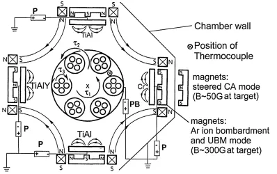
All ion bombardment and coating deposition experiments were performed in an industrial scale combined steered cathodic arc/unbalanced magnetron (CA/UBM) deposition system HAUZER HTC 1000-4-ABS ([98] and [31]), as shown schemati cally in Figure 3.1. The Cr target/cathode (alternatively Ti, Nb or V) is operated in
Chamber wall
0
Position of
Thermocouple
magnets:
steered CA mode
(B~50G at target)
magnets:
Ar ion bombardment
and UBM mode
(B~300Gat target)
s ________ s
IS3 Inj— isi— i n| R 1 W \
&
^ P _ J
sI-J
n| E<1
s
s
F igure 3.1: Schematic cross-section of HAUZER HTC 1000-4-ABS. The four individual power supplies for each cathode are labelled with P and PB stands for the bias power supply. The power supplies for the electro-magnetic coils are not shown.
the steered CA mode using the permanent magnets shown in the withdrawn position
[image:49.614.93.491.308.558.2]Chapter 3: Experimental methods
and TiAlY target/cathodes are used in the UBM mode (B « 300 G) magnetically
coupled to form a closed field for an enhanced ionisation and a high ion current density at the substrate surface. The substrates undergo 3-axis planetary rotation during ion bombardment as well as deposition. The average distance between the targets/cathodes and the substrates is 25 cm. The vacuum chamber is evacuated to
a pressure of 6 x 10⁻³ Pa and heated to a tem perature of 400 °C (measured using a
thermocouple) prior to any plasma experiments in order to minimise target poison ing due to desorption of residual gases (mainly water vapour). The pump down and
heating cycle is followed by a 20 minute (if not stated differently) ion bombardment
step. Five types of experiments were carried out, varying
(I) the ion species (Figure 3.2a),
(II) the ion energy (Figure 3.2b),
(III) exposure time to ion bombardment (Figure 3.3a),
(IV) working gas pressure (Figure 3.3b), and
(V) arc current (Figure 3.3c).
In most cases ion bombardment was followed by the deposition of 100 nm TiAlN. In
addition, samples with 300 nm TiAlN followed by 3.2 fim TiAlYN were fabricated.
For experiment (II) a series of exclusively sputter cleaned samples (no coating de
position) was produced. During ion bombardment the substrate tem perature rises
from 400°C to 450°C for a negative bias voltage Us = 1200 V. In the case of Ar-
ion bombardment and Cr-ion bombardment at lower bias voltage additional radiant heating is required to maintain a tem perature of 450°C. This tem perature was kept constant during the TiAlN reactive deposition process taking place at a gas pressure
of 0.35 Pa (A r/N2 mixture). The gas flow was controlled by a proportional integrat
ing differential controller with feedback to total pressure with a constant Ar flow.
The target power on the two TiAl targets was 8 kW, resulting in the deposition of
Chapter 3: Experimental methods
UBM: Us=75V T=450°C 2x8kW(TiAl): 30 min 3x8kW: 3h 30 min
Cool down
Cool down Target cleaning 2min 3x 1 kW
Target cleaning 2min 3x 1 kW Pump down & heating T=400°C p=6xlO'3Pa Pump down & heating T=400°C p=6xlO'3Pa
UBM: Us=75V T=450°C 2x8kW(TiAl): 10 min
UBM: Us=75V T=450°C 2x8kW(TiAl): 10 min UBM: Us=75V T=450°C
2x8kW(TiAl): 30 min 3x8kW: 3h 30 min
Cr arc
U=600V
lx Ia=100A pAr=6xlO~2Pa
t=20min T->450°C
Cr arc
Us= 1200V lx Ia=100A pAr=6xlO'2Pa
t=20min T->450°C
Cr arc
U=400V
lx Ia=100A pAr=6x 10'2Pa t=20min T->450°C Ar (UBM) Us= 1200V 4x175V pAr=5xlO'‘Pa t=20min T->450°C V arc Us= 1200V lx Ia=100A pAr=6xlO'2Pa
t=20min T->450°C
Ti arc
Us= 1200V 1x1= 100 A pAr=6xlO_2Pa
t=20min T->450°C
Cr arc
U=1000V
1x1= 100 A pAr=6xlO'2Pa t=20min T->450°C Cr arc U=1200V 1x1=100 A pAr=6xlO_2Pa t=20min T->450°C
F igure 3.2: Process parameters: variation of substrate sputter cleaning
Chapter 3: Experimental methods
UBM: Us=75V T=450°C 2x8kW(TiAl): 30 min 3x8kW: 3h 30 min
Cool down Target cleaning 2min 4x 1 kW Pump down & heating T=400°C p = 6 x l0 '3Pa
UBM: Us=75V T=450°C 2x8kW (TiAl): 10 min Cr arc
Us= 1200V lx Ia=100A pAr=6xlO_2Pa
t=10min
T->450°C
Pump down & heating T=400°C p= 6 x !0 '3Pa
Target cleaning 2min 4x 1 kW
C r arc Cr arc U s= 1200V Us=1200V lx Ia= 100A 1x1,=100 A
pAr=9xlO_2Pa, 8min pAr=6xlO'2Pa Pbaser’ ^ min t=10min
T->450°C T->450°C
UBM: U s=75V T=450°C 2x8kW (TiAl): 30 min 3x8kW : 3h 30 min
b
UBM: Us=75V T=450°C 2x8kW (TiAl): 10
Cool down
Pum p dow n & heating T=400°C p = 6 x l0 3Pa
Target cleaning 2min 4x 1 kW
_c
Cr arc U = 1200V lxI=1 0 0 A pAr=6xlO ‘2Pa
t=20m in T->450°C
UBM: Us=75V T=450°C 2x8kW (TiAl): 30 min 3x8kW : 3h 30 ntin
C r arc Us= 1200V
lx Ia=80A
pAr=6xlO '2Pa t=10m in T->450°C
UBM: U s=75V T=450°C
2x8kW (TiAl): 10 min
Cool down
Chapter 3: Experimental methods
In case of the deposition of 3.5/xmnm thick TiAIN based coatings the two TiAl
targets were used at power of 8kW each for 30 minutes. Then 8kW were also
applied to the third (TiAlY) target. TiAlYN deposition was carried out for 210
minutes. Unbalancing coils at a current of 6 A were used for increased ionisation
and to improve the control of the magnetic coupling. The bias voltage during UBM
deposition was routinely Us = 75 V.
3.2
Topography of surfaces
3.2.1 Reflected light microscopy
An Olympus microscope with attached CCD-camera was used. This, together with the analysis 3.0 software, allowed to record digital images. No image processing was performed to enhance the contrast. For maximum contrast a very small aperture size was used.
3.2.2 Atomic force microscopy (AFM )
A METRIS 2000 AFM was used in contact mode. In the AFM the sample is moved
relative to a sharp tip, which is integrated into the end of a cantilever spring. The atomic forces between the sample and the tip are measured employing a laser and detector to measure the cantilever motion. The laser beam is focused on to a split photodiode detector. The beam reflected by the cantilever is then focused onto the middle of the split detector such that the difference signal between the two halves is zero.
Deflection of the cantilever results in a difference of the illumination of th
![Figure 2.2: Cathodic arc evaporation: (a) cathode spot region of a vacuum arc showing neutral, ion, and microdroplet emission (from [24]); (b)effect of weakly bound microdroplets on hole generation in the coating (from [25])](https://thumb-us.123doks.com/thumbv2/123dok_us/777455.583779/24.613.108.516.260.490/figure-cathodic-evaporation-neutral-microdroplet-emission-microdroplets-generation.webp)